Characterization and Modeling of 28-nm FDSOI CMOS Technology down to Cryogenic Temperatures
Abstract
This paper presents an extensive characterization and modeling of a commercial 28-nm FDSOI CMOS process operating down to cryogenic temperatures. The important cryogenic phenomena influencing this technology are discussed. The low-temperature transfer characteristics including body-biasing are modeled over a wide temperature range (room temperature down to 4.2 K) using the design-oriented simplified-EKV model. The trends of the free-carrier mobilities versus temperature in long and short-narrow devices are extracted from dc measurements down to 1.4 K and 4.2 K respectively, using a recently-proposed method based on the output conductance. A cryogenic-temperature-induced mobility degradation is observed on long MOS, leading to a maximum hole mobility around 77 K. This work sets the stage for preparing industrial design kits with physics-based cryogenic compact models, a prerequisite for the successful co-integration of FDSOI CMOS circuits with silicon qubits operating at deep-cryogenic temperatures.
keywords:
28 nm FDSOI, characterization, cryogenic CMOS, cryogenic MOSFET, double-gate, low temperature, mobility, modeling, 4.2 K1 Introduction
The birth of CMOS-compatible qubits in silicon [1, 2, 3, 4] has rebooted the interest in cryogenic CMOS electronics for computing applications. Since the 1970s, MOSFET devices have been under investigation at cryogenic temperatures for use in custom applications, such as low-noise scientific equipment, spacecraft, power conversion etc. [5, 6, 7, 8, 9]. However, despite its many benefits for reaching high-performance and low-power computing [10], cryogenic cooling did not stay into practice for computing, abandoning the trend set by the ETA-10 liquid-nitrogen-cooled supercomputer [11].
Nowadays, co-integrating qubits and CMOS circuits on the same substrate can greatly aid the development of scalable quantum computers featuring massive parallelism and error correction[12, 13, 14]. In this context, a silicon-on-insulator (SOI) platform is particularly attractive since the back gate provides additional control over the electron-spin qubit, trapped under the front gate of a SOI (nanowire) MOSFET[12, 15, 16]. To integrate the control circuits with quantum devices working at deep-cryogenic temperatures, regular SOI MOSFETs need to demonstrate reliable digital, analog and RF functionalities at such low temperatures. Using SOI cryogenic control electronics, the back gate can prove a useful tool to control the threshold voltage and hence the power consumption in circuits integrated close to the qubits [17], benefiting qubit coherence time by lowering generated noise. The main focus is on advanced ultra-thin body fully-depleted SOI (FDSOI) technology, e.g., the 28-nm node, to enable ultimate scalability of the resulting hybrid quantum-classical system [16, 18].
The 28-nm node, presently considered the ideal node for analog and RF applications at room temperature [19], has recently been tested for digital and analog functionality down to liquid-helium temperature (4.2 K) [17], and millikelvin temperature (20 mK) [20]. The improvement in RF characteristics has been verified down to liquid-nitrogen temperature (77 K) [21]. In addition to device characterization, it is mandatory that industry-standard compact models [22, 23, 24] become compatible with cryogenic temperatures, to achieve optimal cryogenic CMOS designs controlling a large number of qubits. To date, important temperature-related phenomena have been included only by fitting the characteristics using the existing temperature-scaling laws available in industry-standard compact MOS transistor models dedicated to room-temperature operation, i.e., for bulk [25] and double-gate MOSFET [26]. However, this approach cannot provide a physically-sound basis to further develop compact models targeting reliable CMOS designs at cryogenic temperatures. Recently, an analytical model for bulk cryogenic MOSFET operation [27] has been proposed, which has been developed starting from the Poisson equation at cryogenic temperatures, validating the Boltzmann statistics and taking into account the temperature dependencies of dopant freeze-out, bandgap widening and the Fermi-Dirac occupation of interface charge traps. This model provides the necessary analytical physics-based expressions for compact modeling purposes at cryogenic temperatures. Furthermore, a body-partitioning technique has been developed which can be used to calculate the extension of the ionized layer of dopants under the gate by field-assisted ionization when the substrate is initially frozen-out at cryogenic temperatures [28]. From this method, it can be expected that the low-doped thin film of silicon in a FDSOI MOSFET can be completely ionized at cryogenic temperature depending on the relative bias points of the front and back gates.
In this work, as an initial investigation prior to further physical and compact modeling, we perform a cryogenic characterization and semi-empirical modeling of a commercial ultra-thin-body 28-nm FDSOI CMOS technology at temperatures down to 4.2 K, similar to earlier work on a commercial 28-nm bulk CMOS technology [29]. The low-temperature dc measurements (transfer and output characteristics) and the characterization down to 4.2 K are presented in Sec. 2 and 3, respectively. In Sec. 2.2, we qualitatively explain the influence of cryogenic temperatures on the electrical behavior of this technology, with a main focus on incomplete ionization (freeze-out) and interface charge traps. The free-carrier mobility trends versus temperature are obtained from the recently-proposed -function method [30], which is derived here for FDSOI technologies (Sec. 3.2). This method allows to extract the mobility from dc transfer or output measurements. In Sec. 4, we illustrate how the drastic temperature reduction, the incomplete ionization, and the interface charge traps can be accounted for in circuit device-models, taking as an example the simplified-EKV model, a simple design-oriented model using only four parameters for short-channel devices.
2 Low-Temperature Measurements
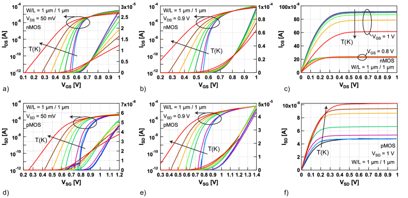
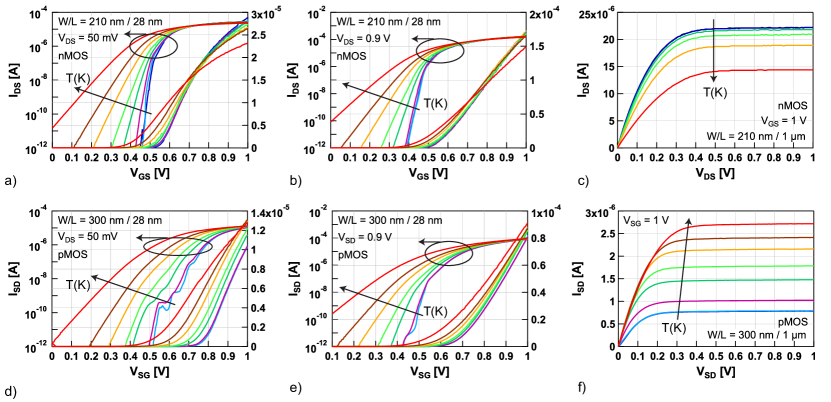
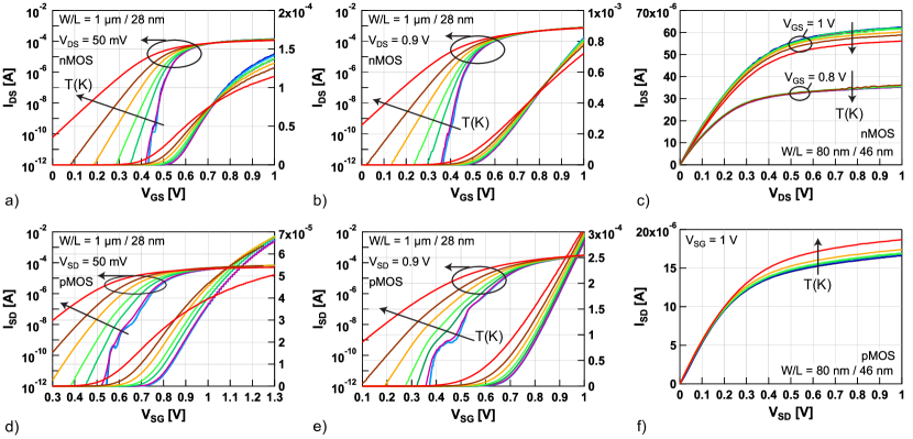
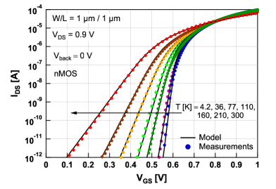
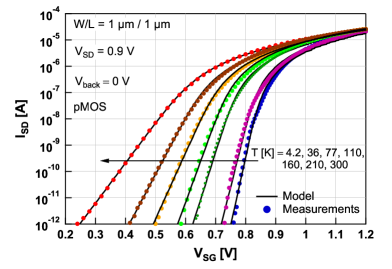
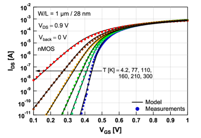
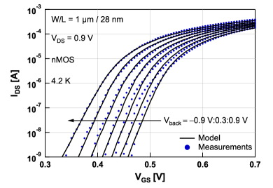
Transfer characteristics in linear ( = 50 mV) and saturation ( = 0.9 V) were measured on various devices of a 28-nm FDSOI CMOS process from room temperature down to 4.2 K, including changes in the body bias [17]. Intermediate temperature steps were taken at 10, 36, 77, 110, 160, and 210 K, and the back-gate voltage () was ramped from 0.9 V to 0.9 V. Output characteristics were measured at zero using the same temperature steps, and additionally at 1.4 K for some devices. Figures (1), (2), and (3) show these measurements for large (Fig. 1), narrow (Fig. 2), and small (Fig. 3) MOS and MOS devices.
2.1 Discussion
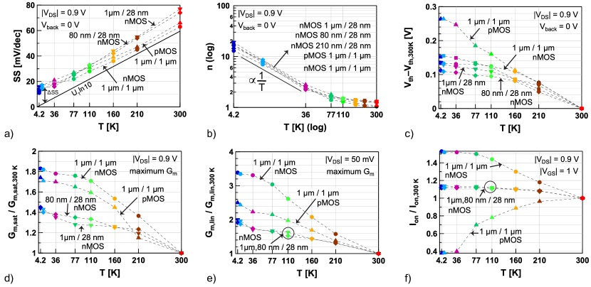
A clear improvement in the subthreshold swing and transconductance is evident for the wide-long MOS and MOS devices in Fig. 1. However, it should be noted that the improvement is minimal between 10 K and 4.2 K with curves lying almost on top of each other. The on-state current increases with decreasing temperature in long MOS, but decreases in long MOS, as highlighted by the opposite temperature trends in the output characteristics in Figs.1-c and 1-f. This will be explained by a cryogenic-temperature-induced mobility degradation in MOS in Sec. 3.2. The fact that the initial slope of the output characteristics in the linear regime (small ) changes with temperature can be used to extract the mobility trend versus temperature down to 1.4 K, according to the -function method described in Sec.3.2. Figure 2 shows similar temperature-dependent dc characteristics for narrow-short and narrow-long devices. However, conductance oscillations are observed on a narrow-short MOS (Fig. 2-d) in the deep-cryogenic range starting from 36 K. These oscillations have been attributed to the presence of dopants diffused from source and drain into the channel [17]. It can be noted that the oscillations becomes less pronounced with increasing temperature, gradually disappearing at 77 K and 110 K (green curves). In Fig. 2 (linear scale) at high gate voltages an impact of access resistance or mobility degradation due to the vertical field is noticeable on narrow-short MOS in the linear regime. In Fig.3, for wide-short MOS, conductance oscillations are also observed. In the output characteristics (Fig. 3-c and 3-f) a drain-induced-barrier-lowering is present at all temperatures, which is roughly temperature dependent. No kink effect is observed in this advanced fully-depleted technology. Since the output conductance in saturation is almost constant with temperature, the intrinsic gain versus temperature will follow the increase in transconductance with decreasing temperature.
2.2 Low-Temperature Phenomena
Important cryogenic phenomena influencing double-gate MOSFET performance have been extensively reviewed by Balestra and Ghibaudo [31, 32, 7], and Claeys and Simoen[8]. These phenomena, also present at room temperature but to a lower degree, include interface traps, dopant incomplete ionization, field-assisted ionization, mobility temperature-trend, bandgap temperature-trend, exponential temperature dependency of the intrinsic carrier concentration, and quantum effects. It should be noted that the kink effect in the output characteristics, prominently present in older technologies at cryogenic temperatures [33], has not been observed in this fully-depleted technology below the used supply voltage. Below follows a brief description of the phenomena which can impact a fully-depleted FDSOI technology, and how to model them:
-
1.
Incomplete ionization or substrate freeze-out In a MOSFET in thermal equilibrium (no voltage applied) dopant atoms will become deionized at a sufficiently low (cryogenic) temperature depending on the doping concentration in the range to [34, 35, 36, 37]. An overview of the freeze-out critical temperatures for each doping concentration in this range in silicon can be found in [28]. At higher doping concentrations, e.g., in the source and drain contacts, no freeze-out happens due to the formation of impurity bands which overlap with the conduction or valence band edges [38]. Therefore, freeze-out does not influence the access resistance improvement at cryogenic temperatures [39]. For a -type silicon body, an acceptor dopant atom will be ionized from a theoretical viewpoint when the acceptor energy is occupied by an electron. Therefore, the ionized dopant concentration, , is given by
(1) where is the ionization probability given by a Fermi-Dirac distribution function, and the electron quasi-Fermi-level is with the channel voltage. The RHS of (1) is convenient for direct inclusion in the Poisson-Boltzmann equation [27].
In FDSOI, the doping concentration is rather low () compared to the inversion charge density. However, as illustrated in Fig. 4-a, in the flatband condition and at 4.2 K, approximately all dopants will be frozen-out, independent of the doping concentration in the range (). The calculated -position at 4.2 K lies under , leading to freeze-out or (Fig. 4-b). Nonetheless, the front-gate voltage will ionize the impurities under the surface of the front-gate, when bends under near the surface of the front-gate. In the subthreshold region, when , complete ionization can be assumed under the front gate. This transition from freeze-out to complete ionization due to the applied field can lead to a kink in early depletion [27]. Note that depending on the band bending at the front and back gates in a certain mode of operation, it is possible that the dopants under the front gate are completely ionized but frozen-out under the back gate or vice versa. A complete comprehension of the field-assisted ionization effect on the mobile charge density in FDSOI below inversion and including body bias, would require a more in-depth physical analysis.
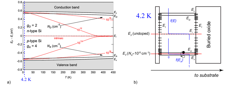
Figure 4: a) Simulated position of the Fermi-level (red) in - and -type doped silicon as a function of temperature and doping concentration. At 4.2 K, the silicon is frozen-out for all doping concentrations in the range ( - ) since or , and and are close to step functions. The temperature dependency of the bandgap from Varshni [40] is used, b) Illustration of freeze-out and interface charge traps in the thin silicon film of a FDSOI MOSFET with a -type body (). The two phenomena can be described by Fermi-Dirac statistics. The position of the Fermi level is shown in red. The probabilities of dopant ionization and interface-trap occupation depend on the position of the Fermi-level in the silicon film with respect to and , respectively. In case bends under near the surface of one of the gates, an ionized layer of dopants forms under the gate. Field-assisted ionization makes before inversion is reached. In the figure it is assumed that the front and back gates are biased such that a flatband situation is created. -
2.
Temperature-dependent occupation of interface charge traps[41, 42] Interface traps need to be included for both the front and the back gate, as illustrated in Fig. 4-b. This adds two additional Fermi-Dirac temperature dependencies (with a trap energy-level at position in the bandgap), apart from the ionization probability . The interface traps can be modeled as a discrete summation of traps, as explained in [43, 44, 45]. The temperature-dependent occupation of interface traps is important for a correct derivation of the subthreshold-swing formula, leading to hyperbolic temperature dependency of the slope factor (ignoring coupling effects between front and back gates), which will be discussed in more detail in Sec. 3.
- 3.
-
4.
Exponential temperature dependency of the intrinsic carrier concentration The intrinsic carrier concentration is given by , which at 4.2 K leads to extremely small values lying outside IEEE double-precision arithmetic, in the order of [27]. This is physically accurate since the overlap of a Fermi-Dirac function at 4.2 K, lying at the intrinsic level (Fig. 4-b), and the density-of-states in the conduction band becomes very small.
-
5.
Quantum confinement and quantum transport Quantum effects become more pronounced in FDSOI MOSFETs at cryogenic temperatures, since they are less obscured by thermal fluctuations when the quantized energy is similar to the thermal energy [46].
3 Characterization
In this section, the following technological parameters are extracted from the cryogenic measurements: the subthreshold swing (), slope factor (), threshold voltage (), transconductance in linear and saturation (), the on-state current (), and the effective free-carrier (electron and hole) mobilities ().
3.1 Subthreshold swing, Threshold voltage, Transconductance, and On-state current
As illustrated in Fig. 5-a, for temperatures below 160 K, the extracted average -values show an increasing offset, , from the thermal limit, , with the thermal voltage. reaches around 10 mV/dec at 4.2 K for long MOS, since predicts 0.8 mV/dec. The slope factors required to reach such high -values are shown in Fig. 5-b (). From this figure a hyperbolic temperature-dependency of is evident, which is not strongly dependent on geometry at cryogenic temperatures. The values below 77 K in Fig. 5-a cannot be explained anymore by , where the slope-factor is limited by two, according to . Here the depletion capacitance is smaller than the oxide capacitance . Furthermore, including the interface-trap capacitance, , i.e. with the density-of-interface-traps per unit area, would lead to very high extracted values for in the order of at 4.2 K [9, 42, 41], and at 20 mK [20]. The latter is higher than the density of surface-states in silicon (). However, it should be emphasized that in this -formula the temperature-dependent occupation of interface-traps is not taken into account (see Sec. 2.2). Reliable extraction of the interface-trap-density at deep-cryogenic and millikelvin temperatures using the standard -formula is therefore questionable. Inclusion of the interface-trap temperature dependency into the subthreshold swing theory of bulk MOSFET has been shown to yield lower extracted -values [27]. Similarly to the derivation for bulk MOSFET presented in [27], by including the temperature dependency of can be derived for the front-gate in FDSOI as well, ignoring the coupling effects between front and back gates. This gives , where is the slope factor without interface traps, and the subthreshold-swing offset as observed in Fig. 5-a. is given by with the density-of-interface-traps and the trap degeneracy factor. Note that in this model, does not become multiplied with , resulting in reasonable extracted values for at cryogenic temperatures lower than found in [41, 42, 20]. The -offset starts to increase below 160 K since the subthreshold region happens when lies closer to , where is observed to be higher already at 300 K (see also Fig. 4-b) [47].
The shift in threshold voltage at 4.2 K with respect to room temperature increases in the order of 0.10.3 V (Fig. 5-c). Note that the largest -increase is observed for MOS, similarly to a 28-nm bulk process[29]. Furthermore, the maximum and (Figs.5d-e) improve down to 4.2 K, e.g. respectively 3.4 (linear) and 1.8 (saturation) for MOS = 1 m / 1 m. In Fig.5-f, is extracted at 1 V. Note that the actual trend of with temperature is strongly dependent on the bias and the device-type. At a standard supply voltage of 1 V, the on-state current increases with decreasing temperature for long MOS (Fig. 1-a-c), while it decreases for MOS (Fig. 1-d-f). However, a cryogenic-temperature-induced mobility degradation has not been extracted from measured CV characteristics on this device [17]. Therefore, in the next section, we take a second look at the characterization of the free-carrier mobility in this technology at cryogenic temperatures.
3.2 Free-Carrier Mobility
In doped bulk silicon, the free-carrier mobility is expected to drop when transitioning below a certain cryogenic temperature and Coulombic impurity scattering becomes dominant over phonon scattering, leading to a typical bell-shaped mobility trend with respect to temperature[38, 5] This behavior can be different in MOSFET devices when the channel is ballistic.
The free-carrier mobility in MOSFETs is usually extracted from dc measurements using the -function approach [48, 49, 50], or from a combination of dc and capacitance measurements using the split- method. For advanced CMOS technologies, the split-CV method can yield unreliable results due to the dominance of extrinsic capacitances, and the -function has two effective slopes. Both methods are also used to characterize advanced devices down to deep-cryogenic ( 10 K) temperatures [51, 52, 32, 17]. Dopant freeze-out and field-assisted ionization may change the dependency of the scattering mechanisms on the gate voltage. Since in strong inversion field-assisted ionization is complete, the underlying assumption of the -function approach, i.e., the homographic gate-voltage dependent mobility law, [48], can still provide an adequate description of the mobility down to cryogenic temperatures. On the other hand, the split- method has to deal with the unknown thermal behavior of the extrinsic capacitances, and requires deep-cryogenic cooling for two types of measurements. Using CV measurements, a mobility degradation at cryogenic temperatures has not been observed for long MOS in this technology [17]. In the next subsection, we obtain the free-carrier mobilities from dc measurements according to an approach recently developed by Jazaeri et al[30].
3.3 Free-Carrier Mobility Extraction using -function
The Jazaeri mobility-extraction method (-function) [30] does not assume any gate-voltage dependent mobility law a priori. The method only assumes drift-diffusion transport in advanced field-effect transistors as a starting point of the derivation [30]. Drift-diffusion transport has been shown to give an accurate representation of the current down to 4.2 K, and the validity of the Boltzmann statistics has been demonstrated down to millikelvin temperatures [28, 27]. Therefore, here we can extend this method to deep-cryogenic temperature operation. In what follows, the method will be briefly derived for SOI technology.
Following the approach in [30], for two different operating points in the linear regime, drift-diffusion gives , and , where is the mean value of the local mobile charge densities at source and drain, i.e., , and it is assumed that is not as a function of for small . Hence we can derive that
| (2) |
in a first approximation. The RHS of (2) can be obtained from dc measurements. Once is known, the mobility can be extracted by merging (2) with the drift-diffusion expression for and eliminating the mobility [30].
In strong inversion, can be estimated as , with the intrinsic gate capacitance per unit area. This expression is still valid down to deep-cryogenic temperatures since (i) the Maxwell-Boltzmann approximation has been verified down to millikelvin temperatures [27], (ii) in the inversion layer all the dopants are ionized due to field-assisted ionization [53, 28], and (iii) interface traps only affect the DC current significantly in the subthreshold region, not in the inversion region [27, 28]. Therefore, following [30]
| (3) |
With (2), we obtain
| (4) |
Thus the mobility is given by
| (5) |
Therefore, for FDSOI the formula remains the same but only the two gate capacitances have to be added. To be very accurate, one would need to consider as a function of temperature, but this would again require CV measurements. However, in the CV characteristics of this technology down to 4.2 K only a change in the threshold voltage has been observed, and not much change in the shape of [17, 54]. Therefore, in strong inversion, we can determine an effective mobility, , setting and . For this reason, in this work we will only investigate mobility-ratios with respect to room temperature, and not the exact values of the mobility. To extract the mobility at a constant back-gate voltage, it is allowed to take into account only the capacitance on the front-gate. This gives
| (6) |
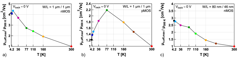
which is valid at small (linear regime) and high (strong inversion) [30]. Expression (6) is referred to as the -function. According to this expression, the mobility is proportional to the curvature of the output characteristics at small at a given gate voltage and temperature. Note the minus sign, leading to a positive mobility-value since is negative. The derivative in (6) can be calculated from the measurements as the difference in initial slopes using a back-difference method (at small ). The method is versatile since the free-carrier mobility can be obtained either from measured output characteristics using (6), or from two linear transfer characteristics (5), depending on which low-temperature data is available. Here we extract the mobility from the output characteristics which are available down to 1.4 K for the long devices, shown in Fig.1-c and 1-f.
Figure 6 plots the ratio of the maximum effective mobility versus the room-temperature mobility for MOS 1 /1 m (Fig. 6-a), MOS 1 /1 m (Fig. 6-b), and MOS 80 nm/46 nm (Fig. 6-c). A mobility degradation is observed for the long devices, where the temperature with maximum mobility is shifted between MOS (10 K) and MOS (77 K). No mobility degradation is observed on short MOS down to 4.2 K.
4 Modeling
In this section, we model the low-temperature measurements (Sec. 2) using the design-oriented simplified EKV model, focusing on the measurements that do not show any oscillations.
A detailed overview of this model is presented in[55, 56]. Its suitability for FDSOI processes has been assessed at room temperature, including body-biasing [57]. The model is valid in saturation, expressing the measured drain current in saturation in terms of an inversion coefficient, , given by , where the specific current, , is defined as , and the ’specific-current-per-square’, , is a parameter independent of dimensions given by . Many analog figure-of-merits can be expressed in terms of this inversion coefficient, which separates the different regions of inversion as follows:
-
1.
: weak inversion
-
2.
: moderate inversion
-
3.
: strong inversion.
The long-channel model is given by the following expression [55, 56]:
| (7) |
and the short-channel model by
| (8) |
where is the normalized pinch-off voltage, the normalized inversion charge at the source (with ), and the normalized source voltage. The velocity saturation parameter, , is the ratio of the channel in full velocity saturation (near the drain) over the total length of the channel.
Starting from the measured drain current in saturation, the inversion coefficient is evaluated for each at a given gate voltage, using a specific model parameter . Depending on the length of the channel, we proceed as follows:
4.1 Procedure long-channel
4.2 Procedure short-channel
For each , the first expression in (8) is numerically solved for , given a specific . The -values are derived from all using the second expression in (8), Similar to the long-channel model, the gate voltage then follows from , given specific and model parameters.
Note that the long-channel model uses three model parameters (, , ), while the short-channel model uses four (, , , ). By plotting versus the obtained , the model curves can be validated with the measurements at each temperature, as will be illustrated in the next section.
| Temperature [K] | n | [V] | [nA] |
|---|---|---|---|
| 4.2 | 13 | 0.605 | 55 |
| 36 | 2.1 | 0.6 | 105 |
| 77 | 1.4 | 0.585 | 195 |
| 110 | 1.21 | 0.57 | 235 |
| 160 | 1.16 | 0.55 | 395 |
| 210 | 1.1 | 0.525 | 515 |
| 300 | 1.07 | 0.485 | 835 |
| Temperature [K] | n | [V] | [nA] |
|---|---|---|---|
| 4.2 | 23 | 0.84 | 42 |
| 36 | 3.07 | 0.825 | 65 |
| 77 | 1.82 | 0.76 | 75 |
| 110 | 1.46 | 0.73 | 105 |
| 160 | 1.25 | 0.695 | 125 |
| 210 | 1.11 | 0.65 | 135 |
| 300 | 1.1 | 0.6 | 235 |
| Temperature [K] | n | [V] | [nA] | [nm] |
|---|---|---|---|---|
| 4.2 | 22 | 0.47 | 75 | 5 |
| 77 | 1.7 | 0.46 | 175 | 8 |
| 110 | 1.47 | 0.45 | 195 | 8.5 |
| 160 | 1.38 | 0.43 | 335 | 9 |
| 210 | 1.34 | 0.41 | 505 | 10 |
| 300 | 1.3 | 0.37 | 835 | 11 |
4.3 Comparison with measurements
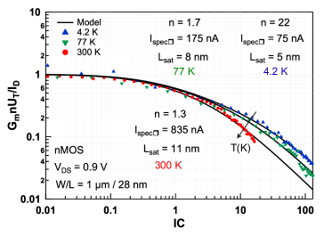
Using the model over a wide temperature range (from 300 down to 4.2 K), the transfer characteristics, back-gate sensitivity, and transconductance efficiency can be accurately modeled in long and short FDSOI devices. Figures 7 to 9 show the modeled transfer characteristics in saturation at all considered temperatures down to 4.2 K at zero back-gate voltage for long MOS (Fig. 7), long MOS (Fig. 8), and short MOS (Fig. 9). The model parameters are shown in the tables below the figures. The strong increase in the model-parameter at deep-cryogenic temperatures corresponds to the interface-trapping process, as explained in Sec. 3. The model-parameter captures the change in the threshold voltage due to Fermi-Dirac scaling and incomplete ionization, increasing in the order of V. Note that the used values for and correspond to the extracted values in Fig. 5-b and 5-c. The model-parameter decreases over one order of magnitude from 300 down to 4.2 K. For the short device, the -parameter decreases from 11 to 5 nm due to a reduction in the phonon scattering, leading to a shorter part of the channel near the drain in velocity saturation. The lower impact of velocity saturation at lower temperatures becomes clear also by plotting the normalized transconductance efficiency, , versus the inversion coefficient at 300, 77, and 4.2 K, shown in Fig. 10. Using the same parameters for , , and as in Fig. 9, good agreement is obtained between the modeled and measured transconductance efficiency at 300, 77, and 4.2 K. Fig. 10 verifies that the design-methodology[58] remains valid for a 28 nm FDSOI technology down to 4.2 K, extending therefore its universality to advanced bulk and FDSOI CMOS operating at extremely-low temperatures. Furthermore, as illustrated in Figures 11 and 12, changing the model parameter allows to capture the effect of the back-gate at 4.2 K for long (11) and short devices. The model parameter tends to increase with increasing absolute values of the back-gate voltage in both long and short devices, accounting for a change in induced by the back gate. The model parameter maintains the same value (5 nm at 4.2 K) for different back-gate voltages, showing that the velocity saturation is not influenced by the back gate.
5 Conclusion
A 28-nm Fully-Depleted SOI CMOS process is characterized and modeled from room temperature down to liquid-helium temperature (4.2 K). Output characteristics and free-carrier mobilities are presented down to 1.4 K. The design-oriented simplified EKV model can accurately predict the impact of the temperature reduction on the transfer characteristics, back-gate sensitivity, and transconductance efficiency of 28-nm devices using four parameters: the slope factor , threshold voltage , specific current , and saturation length . A new method is proposed to extract the free-carrier mobility-trends versus temperature in SOI technology from dc measurements. This method does not require CV measurements and can hence be used to extract the mobility-trend also on short-narrow advanced CMOS devices where parasitic capacitances can dominate. Using this method, a degradation in the free-carrier mobility is observed at cryogenic temperatures in long MOS and MOS, and an increase in a short 46-nm MOS.

| Back-gate Voltage [V] | n | [V] | [nA] |
|---|---|---|---|
| -0.9 | 18 | 0.665 | 115 |
| -0.6 | 17.2 | 0.645 | 90 |
| -0.3 | 14.9 | 0.625 | 68 |
| 0 | 14.9 | 0.608 | 70 |
| 0.3 | 15 | 0.59 | 73 |
| 0.6 | 15.2 | 0.57 | 75 |
| 0.9 | 16 | 0.55 | 105 |
| Back-gate Voltage [V] | n | [V] | [nA] | [nm] |
|---|---|---|---|---|
| -0.9 | 22.8 | 0.522 | 77 | 5 |
| -0.6 | 22.7 | 0.506 | 76 | 5 |
| -0.3 | 22.6 | 0.49 | 75 | 5 |
| 0 | 22.7 | 0.473 | 70 | 5 |
| 0.3 | 23.9 | 0.455 | 80 | 5 |
| 0.6 | 25 | 0.435 | 85 | 5 |
| 0.9 | 29.3 | 0.42 | 115 | 5 |
References
References
- [1] J. J. Pla, K. Y. Tan, J. P. Dehollain, W. H. Lim, J. J. Morton, D. N. Jamieson, A. S. Dzurak, A. Morello, A single-atom electron spin qubit in silicon, Nature 489 (7417) (2012) 541. doi:10.1038/nature11449.
- [2] J. Elzerman, R. Hanson, L. W. Van Beveren, B. Witkamp, L. Vandersypen, L. P. Kouwenhoven, Single-shot read-out of an individual electron spin in a quantum dot, nature 430 (6998) (2004) 431. doi:10.1038/nature02693.
- [3] M. Veldhorst, J. Hwang, C. Yang, A. Leenstra, B. de Ronde, J. Dehollain, J. Muhonen, F. Hudson, K. M. Itoh, A. Morello, et al., An addressable quantum dot qubit with fault-tolerant control-fidelity, Nature nanotechnology 9 (12) (2014) 981. doi:10.1038/nnano.2014.216.
- [4] R. Maurand, X. Jehl, D. Kotekar-Patil, A. Corna, H. Bohuslavskyi, R. Laviéville, L. Hutin, S. Barraud, M. Vinet, M. Sanquer, S. De Franceschi, A CMOS silicon spin qubit, Nature Communications 7 (2016) 13575. doi:10.1038/ncomms13575.
- [5] R. Kirschman, Cold electronics: an overview, Cryogenics 25 (3) (1985) 115 – 122. doi:10.1016/0011-2275(85)90036-0.
- [6] E. A. Gutierrez-D, J. Deen, C. Claeys, Low temperature electronics: physics, devices, circuits, and applications, Academic Press, 2000. doi:10.1016/B978-0-12-310675-9.X5000-2.
- [7] F. Balestra, G. Ghibaudo, Device and Circuit Cryogenic Operation for Low Temperature Electronics, Springer US, 2001. doi:10.1007/978-1-4757-3318-1.
- [8] C. Claeys, E. Simoen, The Perspectives of Silicon-on-Insulator Technologies for Cryogenic Applications, Journal of the Electrochemical Society 141 (9) (1994) 2522–2532. doi:10.1149/1.2055155.
- [9] T. Elewa, F. Balestra, S. Cristoloveanu, I. M. Hafez, J. P. Colinge, A. J. Auberton-Herve, J. R. Davis, Performance and physical mechanisms in SIMOX MOS transistors operated at very low temperature, IEEE Transactions on Electron Devices 37 (1990) 1007–1019. doi:10.1109/16.52436.
- [10] M. Deen, Cryogenic operation of CMOS-based microsystems and computers, Microprocessors and Microsystems 13 (4) (1989) 245 – 253. doi:https://doi.org/10.1016/0141-9331(89)90062-8.
- [11] D. M. Carlson, D. C. Sullivan, R. E. Bach, D. R. Resnick, The ETA 10 liquid-nitrogen-cooled supercomputer system, IEEE Transactions on Electron Devices 36 (8) (1989) 1404–1413. doi:10.1109/16.30952.
- [12] S. R. Ekanayake, T. Lehmann, A. S. Dzurak, R. G. Clark, A. Brawley, Characterization of SOS-CMOS FETs at Low Temperatures for the Design of Integrated Circuits for Quantum Bit Control and Readout, IEEE Transactions on Electron Devices 57 (2) (2010) 539–547. doi:10.1109/TED.2009.2037381.
- [13] D. J. Reilly, Engineering the quantum-classical interface of solid-state qubits, npj Quantum Information 1 (2015) 15011. doi:10.1038/npjqi.2015.11.
- [14] L. Vandersypen, H. Bluhm, J. Clarke, A. Dzurak, R. Ishihara, A. Morello, D. Reilly, L. Schreiber, M. Veldhorst, Interfacing spin qubits in quantum dots and donors—hot, dense, and coherent, npj Quantum Information 3 (1) (2017) 34. doi:10.1038/s41534-017-0038-y.
- [15] L. Hutin, B. Bertrand, R. Maurand, M. Urdampilleta, B. Jadot, H. Bohuslavskyi, L. Bourdet, Y. M. Niquet, X. Jehl, S. Barraud, C. Bäuerle, T. Meunier, M. Sanquer, S. D. Franceschi, M. Vinet, SOI CMOS technology for quantum information processing, in: 2017 IEEE International Conference on IC Design and Technology (ICICDT), 2017, pp. 1–4. doi:10.1109/ICICDT.2017.7993523.
- [16] S. D. Franceschi, L. Hutin, R. Maurand, L. Bourdet, H. Bohuslavskyi, A. Corna, D. Kotekar-Patil, S. Barraud, X. Jehl, Y. M. Niquet, M. Sanquer, M. Vinet, SOI technology for quantum information processing, in: 2016 IEEE International Electron Devices Meeting (IEDM), 2016, pp. 13.4.1–13.4.4. doi:10.1109/IEDM.2016.7838409.
- [17] H. Bohuslavskyi, S. Barraud, M. Cassé, V. Barrai, B. Bertrand, L. Hutin, F. Arnaud, P. Galy, M. Sanquer, S. D. Franceschi, M. Vinet, 28nm Fully-depleted SOI technology: Cryogenic control electronics for quantum computing, in: 2017 Silicon Nanoelectronics Workshop (SNW), 2017, pp. 143–144. doi:10.23919/SNW.2017.8242338.
- [18] P. Clapera, S. Ray, X. Jehl, M. Sanquer, A. Valentian, S. Barraud, Design and Cryogenic Operation of a Hybrid Quantum-CMOS Circuit, Phys. Rev. Applied 4 (2015) 044009. doi:10.1103/PhysRevApplied.4.044009.
- [19] A. Cathelin, Fully Depleted Silicon on Insulator Devices CMOS: The 28-nm Node Is the Perfect Technology for Analog, RF, mmW, and Mixed-Signal System-on-Chip Integration, IEEE Solid-State Circuits Magazine 9 (4) (2017) 18–26. doi:10.1109/MSSC.2017.2745738.
- [20] P. Galy, P. Lemieux, J. C. Lemyre, F. Arnaud, D. Drouin, M. Pioro-Ladrière, Cryogenic temperature characterization of a 28 nm FD-SOI dedicated structure for advanced CMOS and quantum technologies co-integration, IEEE Journal of the Electron Devices Society (2018) 1–1doi:10.1109/JEDS.2018.2828465.
- [21] B. K. Esfeh, M. Masselus, N. Planes, M. Haond, J. P. Raskin, D. Flandre, V. Kilchytska, 28 FDSOI analog and RF Figures of Merit at cryogenic temperatures, in: 2018 Joint International EUROSOI Workshop and International Conference on Ultimate Integration on Silicon (EUROSOI-ULIS), 2018, pp. 1–3. doi:10.1109/ULIS.2018.8354735.
- [22] T. Poiroux, O. Rozeau, P. Scheer, S. Martinie, M. A. Jaud, M. Minondo, A. Juge, J. C. Barbé, M. Vinet, Leti-UTSOI2.1: A Compact Model for UTBB-FDSOI Technologies Part II: Interface Potentials Analytical Model, IEEE Transactions on Electron Devices 62 (9) (2015) 2760–2768. doi:10.1109/TED.2015.2458336.
- [23] T. Poiroux, O. Rozeau, P. Scheer, S. Martinie, M. A. Jaud, M. Minondo, A. Juge, J. C. Barbé, M. Vinet, Leti-UTSOI2.1: A Compact Model for UTBB-FDSOI Technologies Part II: DC and AC Model Description, IEEE Transactions on Electron Devices 62 (9) (2015) 2760–2768.
- [24] S. Khandelwal, Y. S. Chauhan, D. D. Lu, S. Venugopalan, M. A. U. Karim, A. B. Sachid, B. Y. Nguyen, O. Rozeau, O. Faynot, A. M. Niknejad, C. C. Hu, BSIM-IMG: A Compact Model for Ultrathin-Body SOI MOSFETs With Back-Gate Control, IEEE Transactions on Electron Devices 59 (2012) 2019–2026. doi:10.1109/TED.2012.2198065.
- [25] A. Akturk, M. Holloway, S. Potbhare, D. Gundlach, B. Li, N. Goldsman, M. Peckerar, K. P. Cheung, Compact and Distributed Modeling of Cryogenic Bulk MOSFET Operation, IEEE Transactions on Electron Devices 57 (6) (2010) 1334–1342. doi:10.1109/TED.2010.2046458.
- [26] A. Akturk, M. Peckerar, M. Dornajafi, N. Goldsman, K. Eng, T. Gurrieri, M. S. Carroll, Impact Ionization and Freeze-Out Model for Simulation of Low Gate Bias Kink Effect in SOI-MOSFETs Operating at Liquid He Temperature, in: 2009 International Conference on Simulation of Semiconductor Processes and Devices, 2009, pp. 1–4. doi:10.1109/SISPAD.2009.5290227.
- [27] A. Beckers, F. Jazaeri, C. Enz, Cryogenic MOS Transistor Model, IEEE Transactions on Electron Devices 65 (9) (2018) 3617–3625. doi:10.1109/TED.2018.2854701.
- [28] A. Beckers, F. Jazaeri, C. Enz, Characterization and Modeling of 28 nm Bulk CMOS Technology down to 4.2 K, IEEE Journal of the Electron Devices Society (2018) 1–1doi:10.1109/JEDS.2018.2817458.
- [29] A. Beckers, F. Jazaeri, A. Ruffino, C. Bruschini, A. Baschirotto, C. Enz, Cryogenic characterization of 28 nm bulk CMOS technology for quantum computing, in: 47th European Solid-State Device Research Conference (ESSDERC), 2017, pp. 62–65. doi:10.1109/ESSDERC.2017.8066592.
- [30] F. Jazaeri, A. Pezzotta, C. Enz, Free Carrier Mobility Extraction in FETs, IEEE Transactions on Electron Devices 64 (12) (2017) 5279–5283. doi:10.1109/TED.2017.2763998.
- [31] Brief review of the MOS device physics for low temperature electronics, Solid-State Electronics 37 (12) (1994) 1967 – 1975. doi:https://doi.org/10.1016/0038-1101(94)90064-7.
- [32] F. Balestra, G. Ghibaudo, Physics and performance of nanoscale semiconductor devices at cryogenic temperatures, Semiconductor Science and Technology 32 (2) (2017) 023002.
- [33] B. Dierickx, L. Warmerdam, E. R. Simoen, J. Vermeiren, C. Claeys, Model for hysteresis and kink behavior of MOS transistors operating at 4.2 K, IEEE Transactions on Electron Devices 35 (7) (1988) 1120–1125. doi:10.1109/16.3372.
- [34] D. P. Foty, Impurity ionization in MOSFETs at very low temperatures, Cryogenics 30 (12) (1990) 1056 – 1063. doi:https://doi.org/10.1016/0011-2275(90)90207-S.
- [35] E. Simoen, B. Dierickx, L. Warmerdam, J. Vermeiren, C. Claeys, Freeze-out effects on NMOS transistor characteristics at 4.2 K, IEEE Transactions on Electron Devices 36 (6) (1989) 1155–1161. doi:10.1109/16.24362.
- [36] R. F. Pierret, G. W. Neudeck, Advanced semiconductor fundamentals, Vol. 6, Addison-Wesley Reading, MA, 1987.
- [37] F. Balestra, L. Audaire, C. Lucas, Influence of substrate freeze-out on the characteristics of MOS transistors at very low temperatures, Solid-State Electronics 30 (3) (1987) 321 – 327. doi:https://doi.org/10.1016/0038-1101(87)90190-0.
- [38] A. K. Jonscher, Semiconductors at cryogenic temperatures, Proceedings of the IEEE 52 (10) (1964) 1092–1104. doi:10.1109/PROC.1964.3296.
- [39] A. Akturk, J. Allnutt, Z. Dilli, N. Goldsman, M. Peckerar, Device Modeling at Cryogenic Temperatures: Effects of Incomplete Ionization, IEEE Transactions on Electron Devices 54 (11) (2007) 2984–2990. doi:10.1109/TED.2007.906966.
- [40] Temperature dependence of the energy gap in semiconductors, Physica 34 (1) (1967) 149 – 154. doi:https://doi.org/10.1016/0031-8914(67)90062-6.
- [41] I. M. Hafez, G. Ghibaudo, F. Balestra, Assessment of interface state density in silicon MOS transistors at room, liquid nitrogen, and liquid helium temperatures, Journal of Applied Physics (4). doi:10.1063/1.345572.
- [42] R. Trevisoli, M. de Souza, R. T. Doria, V. Kilchtyska, D. Flandre, M. A. Pavanello, Junctionless nanowire transistors operation at temperatures down to 4.2 K, Semiconductor Science and Technologydoi:10.1088/0268-1242/31/11/114001.
- [43] A. Yesayan, F. Jazaeri, J. M. Sallese, Charge-Based Modeling of Double-Gate and Nanowire Junctionless FETs Including Interface-Trapped Charges, IEEE Transactions on Electron Devices 63 (3) (2016) 1368–1374. doi:10.1109/TED.2016.2521359.
- [44] F. Jazaeri, J.-M. Sallese, Modeling Nanowire and Double-Gate Junctionless Field-Effect Transistors, Cambridge University Press, 2018. doi:10.1017/9781316676899.
- [45] F. Jazaeri, C. M. Zhang, A. Pezzotta, C. Enz, Charge-Based Modeling of Radiation Damage in Symmetric Double-Gate MOSFETs, IEEE Journal of the Electron Devices Society 6 (1) (2018) 85–94. doi:10.1109/JEDS.2017.2772346.
- [46] J. P. Colinge, A. J. Quinn, L. Floyd, G. Redmond, J. C. Alderman, W. Xiong, C. R. Cleavelin, T. Schulz, K. Schruefer, G. Knoblinger, P. Patruno, Low-temperature electron mobility in Trigate SOI MOSFETs, IEEE Electron Device Letters 27 (2) (2006) 120–122. doi:10.1109/LED.2005.862691.
- [47] Attojoule MOSFET logic devices using low voltage swings and low temperature, Solid-State Electronics 28 (3) (1985) 255 – 276. doi:https://doi.org/10.1016/0038-1101(85)90006-1.
- [48] G. Ghibaudo, New method for the extraction of MOSFET parameters, Electronics Letters 24 (9) (1988) 543–545. doi:10.1049/el:19880369.
- [49] A. Emrani, F. Balestra, G. Ghibaudo, On the understanding of electron and hole mobility models from room to liquid helium temperatures, Solid-State Electronics 37 (10) (1994) 1723 – 1730. doi:https://doi.org/10.1016/0038-1101(94)90219-4.
- [50] M. Shin, M. Shi, M. Mouis, A. Cros, E. Josse, G. T. Kim, G. Ghibaudo, Low-temperature characterization of 14 nm FDSOI CMOS devices, in: Low Temperature Electronics (WOLTE), 2014. doi:10.1109/WOLTE.2014.6881018.
- [51] C. L. Huang, G. S. Gildenblat, Measurements and modeling of the n-channel MOSFET inversion layer mobility and device characteristics in the temperature range 60-300 K, IEEE Transactions on Electron Devices 37 (5) (1990) 1289–1300. doi:10.1109/16.108191.
- [52] Split C-V measurements of low temperature MOSFET inversion layer mobility, Cryogenics 29 (12) (1989) 1163 – 1166. doi:https://doi.org/10.1016/0011-2275(89)90296-8.
- [53] A. Beckers, F. Jazaeri, H. Bohuslavskyi, L. Hutin, S. D. Franceschi, C. Enz, Design-oriented modeling of 28 nm FDSOI CMOS technology down to 4.2 K for quantum computing, in: 2018 Joint International EUROSOI Workshop and International Conference on Ultimate Integration on Silicon (EUROSOI-ULIS), 2018, pp. 1–4. doi:10.1109/ULIS.2018.8354742.
- [54] A. Akturk, N. Goldsman, Z. Dilli, M. Peckerar, Effects of cryogenic temperatures on small-signal MOSFET capacitances, in: 2007 International Semiconductor Device Research Symposium, 2007, pp. 1–2. doi:10.1109/ISDRS.2007.4422237.
- [55] C. Enz, F. Chicco, A. Pezzotta, Nanoscale MOSFET Modeling: Part 1: The Simplified EKV Model for the Design of Low-Power Analog Circuits, IEEE Solid-State Circuits Magazine 9 (3) (2017) 26–35. doi:10.1109/MSSC.2017.2712318.
- [56] C. Enz, F. Chicco, A. Pezzotta, Nanoscale MOSFET Modeling: Part 2: Using the Inversion Coefficient as the Primary Design Parameter, IEEE Solid-State Circuits Magazine 9 (4) (2017) 73–81. doi:10.1109/MSSC.2017.2745838.
- [57] A. Pezzotta, F. Jazaeri, H. Bohuslavskyi, L. Hutin, C. Enz, A design-oriented charge-based simplified model for FDSOI MOSFETs, in: 2018 Joint International EUROSOI Workshop and International Conference on Ultimate Integration on Silicon (EUROSOI-ULIS), 2018, pp. 1–4. doi:10.1109/ULIS.2018.8354764.
- [58] F. Silveira, D. Flandre, P. G. A. Jespers, A Gm/ID-based methodology for the design of CMOS analog circuits and its application to the synthesis of a silicon-on-insulator micropower OTA, IEEE Journal of Solid-State Circuits 31 (9) (1996) 1314–1319. doi:10.1109/4.535416.