Multi-beam RF accelerators for ion implantation ††thanks: This work was supported by the US Department of Energy through the ARPA-E ALPHA program and the Energy I-Corps program under contract DE-AC0205CH11231.
Abstract
We report on the development of a radio frequency (RF) linear accelerator (linac) for multiple-ion beams that is made from stacks of low cost wafers. The accelerator lattice is comprised of RF-acceleration gaps and electrostatic quadrupole focusing elements that are fabricated on 4” wafers made from printed circuit board or silicon. We demonstrate ion acceleration with an effective gradient of about with an array of beams. The total ion beam energies achieved to date are in the range with total ion currents in tests with noble gases of . We discuss scaling of the ion energy (by adding acceleration modules) and ion currents (with more beams) for applications of this multi-beam RF linac technology to ion implantation and surface modification of materials.
Index Terms:
Linear accelerators, ion implantationI Introduction
Ion implantation is a mature technology [1]. In most implanters, a single ion beam is formed by extraction of ions from an ion source. Ions are then accelerated and a desired species is selected for implantation. The achievable ion current density is limited by space charge forces and the total ion current is limited by the size of the extraction aperture from which ions can be extracted to form a beam with low enough emittance for efficient transport in the beam line [2]. The concept of multi-beam ion accelerators was developed in the late 1970s by Maschke et al. with the concept of a Multiple Electrostatic Quadrupole Linear Accelerator (MEQALAC) [3]. MEQALACs are RF-driven linear accelerators where the total ion current can be scaled by adding more beams and the ion kinetic energy can be increased by adding accelerator modules. In the first implementations, MEQALACs used RF-cavities to achieve ion acceleration with high voltages driven at frequencies in the range [4]. Multi-beam RF-linacs can boost the total current for applications where beams of mass analyzed single species are required. We have recently reported on the development of multi-beam RF accelerators that we assemble from stacks of low cost wafers [5, 6]. We form RF-acceleration structures and electrostatic quadrupole (ESQ) focusing elements on printed circuit board and silicon wafers with 10-cm diameter using standard microfabrication techniques [7]. In this article we report on the use of compact GaN based RF amplifiers to accelerate ions in an array of beams with energy gains of up to per RF-acceleration unit. This method for generating RF-acceleration voltages leads to an effective acceleration gradient of about in our multi-beam RF linac. While this is much lower than for conventional RF accelerators based on cavities, our implementation is very compact with high current density and is formed from low cost components in a modular architecture.
Figure 1 shows a schematic and a photo of the wafer based multi-beam RF-linac. Ions are extracted from a array of apertures ( diameter) from a filament driven multi-cusp ion source and accelerated to 5 to . We use argon and helium ions for beam tests and the ion source can also provide ions of common dopant species. Following a matching section comprised of a series of ESQ focusing elements, the ion beams reach the lattice of RF acceleration units and ESQs. We determine the energy gain by scanning the bias on a retarding grid while monitoring the ion current in a Faraday cup.
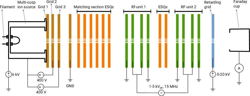
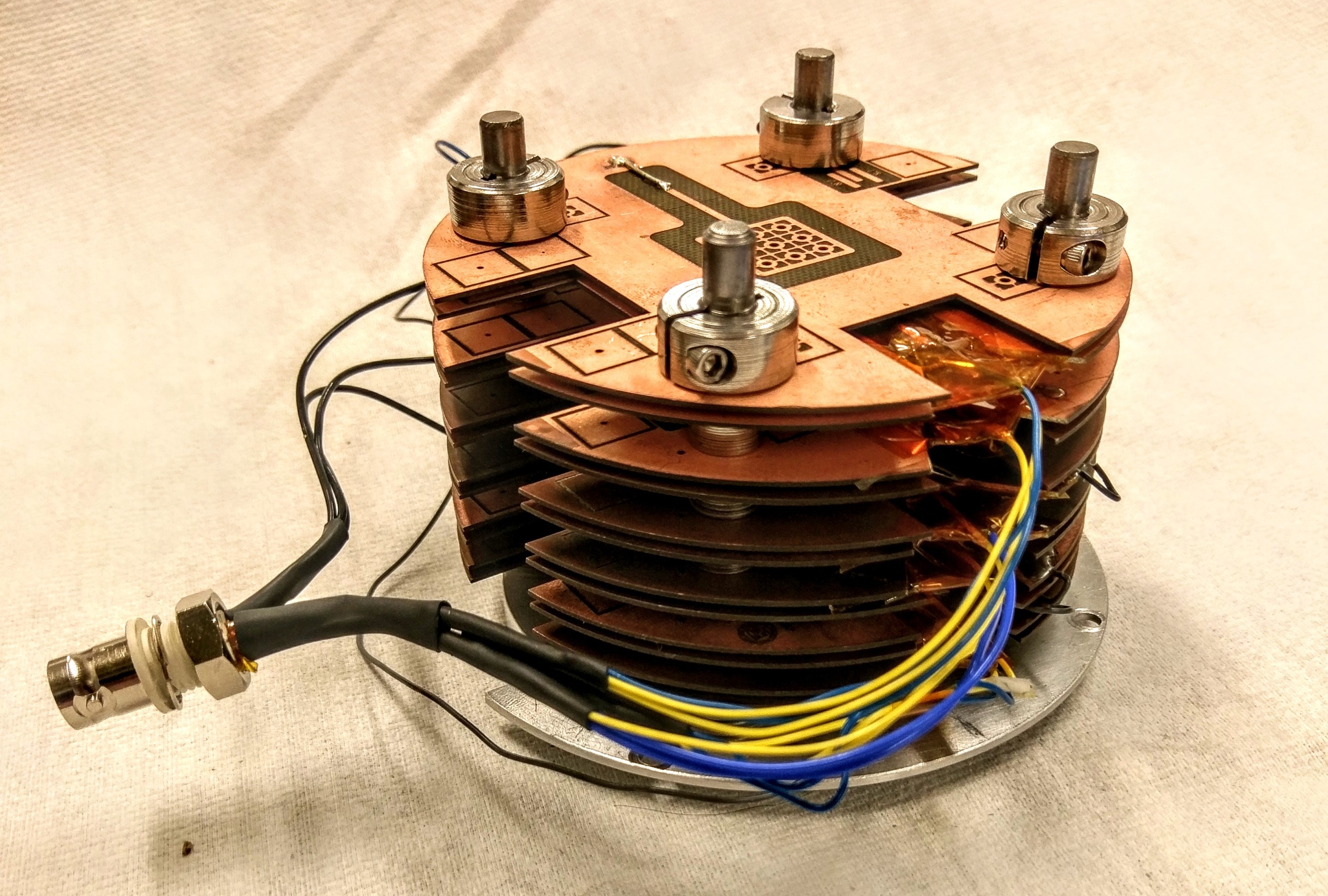
The RF acceleration units are formed from four wafers, with the outside wafers held at ground and the central two wafers driven by high voltage pulses at the selected RF frequency. Ions entering an RF acceleration unit are accelerated by the RF voltage and then drift in the field-free gap between the two central wafers before further acceleration in the gap between the third wafer and the grounded last wafer in the RF acceleration unit. The drift distance is set to match the phase advance of the RF at a given frequency according to , where is the gap distance, the ion velocity and the RF frequency. For operation at with argon ions injected at () the drift distances are . After several stages of acceleration the RF frequency can be increased to compensate for increasing ion velocities and to keep drift distances small. In our first proof-of-concept of this approach of multi-beam ion acceleration we used an external LC-tank circuit to generate RF acceleration voltages of 600 V/gap [5]. We have now implemented compact GaN based RF sources [8] that are placed near the acceleration wafers inside the vacuum chamber. The high voltage pulses are delivered through low capacitance wires to the RF acceleration wafers. One RF source can drive ion acceleration in several modules with up to per acceleration gap.
II RF source
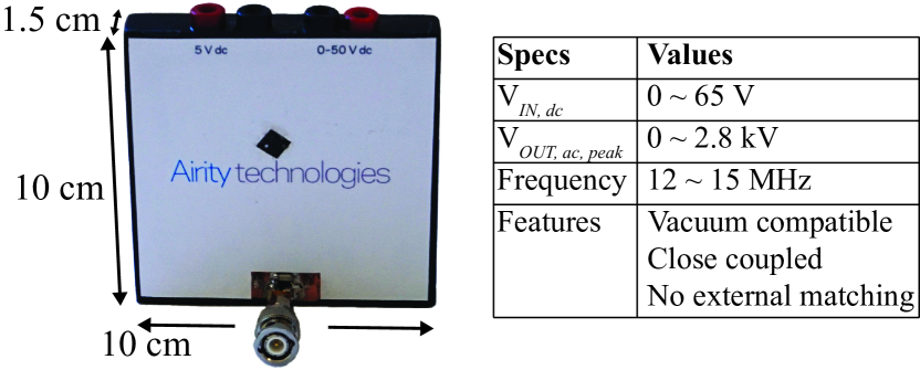
A custom RF power source was developed by Airity technologies to generate the high voltage AC required to drive the wafer array. By leveraging the intrinsic inductive and capacitive elements of the wafers and incorporating them into the source design, a compact and efficient vacuum compatible RF source was built that enables placement close to the wafer array to minimize cable effects. The specifications of the source are summarized in Figure 2.
Initial tests of an updated RF source design suggest that voltages exceeding are possible. Future work will further investigate such designs with the goal of scaling array voltage to .
III Modeling
To simulate the system and investigate its scaling behaviour an equivalent circuit was developed. The RF source was modeled as a simple circuit shown in Figure 3. Since the RF source has been developed to drive a load, the capacitance in the model has been split into an internal capacitance, , and the external load. In our case our load of a single RF unit is smaller than the load for which the unit was designed and we therefore augmented the load capacitance with a parallel capacitor, . When driving more units this capacitor should be adjusted accordingly. The resistor in the source model varies with the driving voltage. This was added to compensate for the observed behaviour of lower gains at higher voltages, possibly due to heating of the RF driver.

The RF units were modeled as a series of cables with inductance and capacitance. The acceleration gaps were modeled as purely capacitive and since the wafers are connected with a short wire loop, a inductance was added between them. The complete circuit is shown in Figure 4. The circuit model includes a capacitance to represent the BNC connector, a cable resistance (the cable resistance was placed to the left of the capacitor due to requirements of the simulations software), a test resistor (see below), a network of capacitors and inductors to represent the cable from the RF source to the wafers, and the capacitance of the acceleration gap including an inductance that represents the ground connection between the wafers.
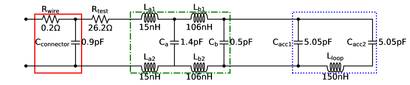
To fit the parameters of the models, a RF unit was analyzed using a vector network analyzer (VNA), Keysight Technology N9923A, in the frequency range of - and also in the range -. Furthermore, the capacitance was measured directly. The VNA measurement ( mode) showed a resonance behaviour around which allowed us to calculate the inductance using the measured capacitance. Furthermore, since we know the source impedance of the VNA (), we can calculate the load impedance at, for example, and from there estimate the resistance. However, due to the small resistance of the system, it is difficult to measure this value directly. We therefore added a known resistor, , to the system, which made it easier to estimate the total resistance using the VNA. The estimated value is in agreement with direct measurements and with calculated values when taking the skin effect into account.
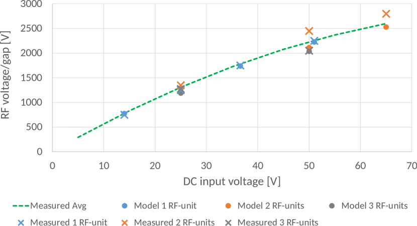
Simulating the modelled circuits using LTspice [9] and Matlab RF toolbox gave good agreement in the frequency range of operation (around ) with an error between measurement and simulation smaller than .
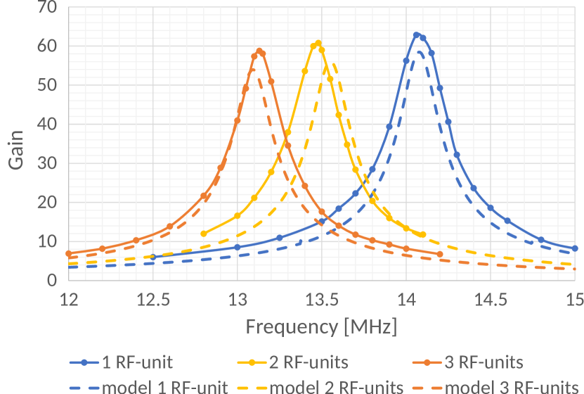
Furthermore, the RF source allowed measurement of the output voltage using a voltage monitor output and we were also able to measure the voltage directly using a high voltage probe (Tektronix P6015A). Figure 5 compares the simulated and measured results when one to three RF units are used. The figure also shows that there is a slight shift in resonance frequency. This is due to the fact that we did not change the capacitor to optimally balance the load impedance of the RF source. This can also explain the slight decrease in gain between the different setups.
IV Beam Experiment
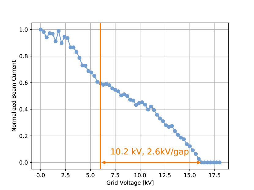
The beam energy was measured using the same setup and method as described previously[5]. Ions were produced using a filament-driven ion source operated with argon at a pressure of (). The source was floated at a high voltage of and ions were extracted from a array of extraction apertures using an extraction voltage of . The ions are then accelerated to ground potential where they enter the RF units. Here, the ions are either accelerated or decelerated depending on their arrival time with respect to the phase of the RF voltage in the acceleration gaps. In our experiments we utilized a long pulse () compared to the RF frequency whereas in a final implementation of the accelerator one would bunch the beam and only inject beam packages at the correct phase. We then select ions above a certain beam energy using a deceleration grid and measure the beam current in a Faraday cup. Due to the almost continuous beam injection, we expect a distribution of beam energies that we can model using a 1D simulation code. The length of the drift sections were chosen for optimal transport of the accelerated ions. We can therefore either fit the beam energy using the simulation code or read of the maximal beam energy gain and divide this by the number of acceleration gaps to get the applied RF voltage. Experiments were carried out using one to three RF units.
Figure 6 shows the result of such a voltage scan on the retarding grid for a system using two RF units (four acceleration gaps). The initial beam energy was and one can clearly see that due to the continuous injection we measure all beam energies from 0-. The maximum energy gain was equivalent to an applied voltage of per acceleration gap. The signal agrees well with our expectation from a 1d model [5].
V Outlook
Using the circuit model we estimate that with the present RF source we will be able to drive nine RF-units in parallel by placing the RF source inside the vacuum system nearby the acceleration gaps. Simulations show that to achieve this one has to take care to minimize the capacitance in the cables connecting the RF units to the RF source. This is due to the fact that the capacitance of the cables for nine RF units will be a considerable part of the load that we need to drive. To minimize phase shift and cable length, we assume that three commercial coax cables will be used in parallel from the RF source which will then split into individual cables to each board. Our simulation was based on coax cables with an impedance of and a low capacitance.
Furthermore, several possible optimization opportunities in our current design of the RF units became clear. First of all, we should be able to further reduce the capacitance of the acceleration gaps by reducing the amount of copper used and secondly higher-rated high-voltage connectors should be used to withstand the higher anticipated voltages per gap. Custom RF cables could further lower the total load capacitance.
VI conclusion
Voltages of per acceleration gap were achieved using a new, compact, near-board RF driver. We believe that optimizing the RF driver specifically for this application will allow us to double or triple the achieved voltage in the near future, and RF acceleration voltages of about /gap might be achievable in the future. Furthermore, a model was developed and compared to measurements that allowed us to model scaling behaviour of the system to higher numbers of RF units. The simulations indicated that up to nine RF units using the current setup can be driven by a single RF source in parallel. By further optimizing the system we believe that this number can also be increased.
The demonstration of RF acceleration voltages of several kV/gap and the near-board RF driver is an important step in the development of a compact and low cost multi-beam accelerator technology that can be scaled to very high beam currents. We estimate that we can accelerate ions in an array of at least beams with a 4” wafer platform for a total current (from an ion source with current density of ). With optimization of the RF drivers, acceleration gradients of over about can be implemented, resulting in a compact, high power accelerator for applications in materials processing.
VII acknowledgements
We thank Michael Current for his encouragement and advice on the evolving field of high-energy ion implantation.
References
- [1] R. W. Hamm and M. E. Hamm, Eds., Industrial Accelerators and Their Applications. World Scientific, 2012.
- [2] I. Brown, Ed., The physics and technology of ion sources. Wiley, 2004.
- [3] A. Maschke, “Meqalac: a new approach to low beta acceleration,” Technical report BNL-51029, June 1979. [Online]. Available: https://www.osti.gov/scitech/servlets/purl/5914442
- [4] W. Urbanus, R. Wojke, J. Bannenberg, H. Klein, A. Schempp, R. Thomae, T. Weis, and P. V. Amersfoort, “Meqalac: A 1-mev multichannel rf-accelerator for light ions,” Nuclear Instruments and Methods in Physics Research Section B: Beam Interactions with Materials and Atoms, vol. 37-38, pp. 508 – 511, 1989. [Online]. Available: http://www.sciencedirect.com/science/article/pii/0168583X89902346
- [5] A. Persaud, Q. Ji, E. Feinberg, P. A. Seidl, W. L. Waldron, T. Schenkel, A. Lal, K. B. Vinayakumar, S. Ardanuc, and D. A. Hammer, “A compact linear accelerator based on a scalable microelectromechanical-system rf-structure,” Review of Scientific Instruments, vol. 88, p. 063304, 2017. [Online]. Available: http://aip.scitation.org/doi/10.1063/1.4984969
- [6] P. A. Seidl, A. Persaud, W. Ghiorso, Q. Ji, W. L. Waldron, A. Lal, K. B. Vinayakumar, and T. Schenkel, “Source-to-accelerator quadrupole matching section for a compact linear accelerator,” Rev. Sci. Instrum., vol. 89, no. 5, p. 053302, May 2018. [Online]. Available: https://doi.org/10.1063/1.5023415
- [7] K. Vinayakumar, A. Persaud, Q. Ji, P. Seidl, T. Schenkel, and A. Lal, “Waferscale electrostatic quadrupole array for multiple ion beam manipulation,” in IEEE proceedings of MEMS 2018, 2018.
- [8] Airity Technologies, Inc., https://www.airitytech.com/, 2018.
- [9] Analog Devices, http://www.analog.com/en/design-center/design-tools-and-calculators/ltspice-simulator.html, 2018, [Online; accessed May 2018].