The Impact of On-chip Communication on Memory Technologies for Neuromorphic Systems
Abstract
Emergent nanoscale non-volatile memory technologies with high integration density offer a promising solution to overcome the scalability limitations of CMOS-based neural networks architectures, by efficiently exhibiting the key principle of neural computation. Despite the potential improvements in computational costs, designing high-performance on-chip communication networks that support flexible, large-fanout connectivity remains as daunting task. In this paper, we elaborate on the communication requirements of large-scale neuromorphic designs, and point out the differences with the conventional network-on-chip architectures. We present existing approaches for on-chip neuromorphic routing networks, and discuss how new memory and integration technologies may help to alleviate the communication issues in constructing next-generation intelligent computing machines.
-
Sep 2018
1 Introduction
Neuromorphic computing is an inter-disciplinary area of research, aiming to emulate the computational principles of Biological neural systems and to utilize such principles to solve complex and computationally intensive problems. The discipline originated with the goal of constructing silicon models of Biological neurons and synapses, based on the observation that the basic Physics governing the flow of current across a semiconductor junction and Biological “junction” in an ion channel were the same [1]. Early papers in the field include the design of silicon models of the retina and cochlea, with analog CMOS circuits emulating Biological circuits discovered through anatomical studies [3, 2, 4, 5, 6].
Concurrently, neural networks were being used for pattern recognition, where neurons were modeled using the McCulloch-Pitts model [7]. In this approach, a neuron is a function that partitions points in space into two regions by a separating hyperplane. Mathematically, a neuron computes a dot product between its weight vector and an input vector, and the output is given by the sign of the result. Generalizations of this where the output is computed using sigmoids or other functional forms were also studied [8]. More recently, such neural networks with a large number of parameters (millions, if not more) have been used to achieve unsurpassed classification accuracy for tasks such as object labeling, face detection, speech processing, etc. Sometimes work in this area is also referred to as “neuromorphic,” since it can trace its roots to Biology as well. In what follows, we do not examine these more recent “deep neural networks,” since while the neurons have Biological connections, the communication structure they use is engineered for functionality, without any attempt to mimic Biology. Neuromorphic systems can be modeled entirely in software, and several projects have developed tools to model Biological neurons, synapses, axons, and dendrites at varying levels of detail [9, 10, 11]. However, such systems are very slow. Even a simplified model of Biological neural networks implemented on a massively parallel machine ran 10 slower than real-time, and consumed 655 kW of power [12]. A Biological system of the same complexity takes five orders of magnitude less power while operating in real-time. Hence, in order to explore the potential of Biologically-inspired computing systems for solving real-world problems, new types of energy-efficient devices and hardware architectures with high scalability factors are required. A domain where such systems could have a large impact is the Internet of Things (IoT), where small form-factor battery operated devices could be enhanced with capabilities akin to the sensory system (e.g. vision or speech recognition) of Biological systems.
Hardware neuromorphic computing systems [13, 18, 19, 20, 14, 17, 15, 16, 21] contain structures that model neurons, synapses, and the connectivity between neurons and synapses. Current large-scale systems have been implemented using conventional CMOS technology, and there has been a large body of work in recent years on novel memory devices for reducing the power consumption in neuromorphic systems. We begin with a brief overview of this body of work (Section 2), summarizing the focus of researchers developing novel devices for neuromorphic system. We then present the problem of implementing connectivity in neuromorphic systems and discusses some of the issues involved in building large-scale neuromorphic hardware that can model millions of neurons (Section 3). We argue that the cost of communication in such systems is extremely high due to the complexity of supporting flexible high-fanout connectivity. This is consistent in what has been observed in existing large-scale neuromorphic systems (Section 4). We discuss what new materials/device technologies might be able to do to alleviate this problem (Section 5), and provide possible directions for future research in this area.
Our primary thesis is that almost all the recent work in memory technologies and materials/device design for neuromorphic systems cannot have a major impact on the system-level power consumption of large-scale neuromorphic systems without new techniques being developed to address the communication problem. When examining the complete system, it is quite clear that the focus of device researchers has been on only a portion of the total power requirement; a non-trivial fraction of the total power budget remains unaddressed, limiting the benefits of the proposed device technologies in isolation.
2 Resistive memory technologies for neuromorphic systems
Most prominent large-scale neuromorphic projects have employed commercial CMOS technology for implementing neural principles. In recent years, there has been growing research efforts to utilize emergent memory and device technologies for scaling up neuromorphic hardware systems. In neuromorphic engineering, most such technologies are primary considered for implementing synaptic and learning models. However, there is a potential to utilize nanoscale emergent devices to overcome the interconnects limitations [24] in 2D /3D VLSI integrations. In recent neuromorphic designs [26, 17, 13], the communication and standby power has become a significant portion of total power consumption. In this section we review most relevant research articles that have investigated the potential of two-terminal emergent devices in improving the performance of CMOS neuromorphic computing systems.
Multiple emergent memory devices have been recently proposed to overcome the limitations of the conventional CMOS memories [30] in embedded systems. Memory resistive (memristor) elements, oxide-based resistive random access memory (oxRAM), conductive-bridging random access memory (CBRAM), phase-change memory (PCRAM) are examples of the emergent memory devices that are explored for integrating with CMOS-based neuromorphic circuits. The characterizations of these memory devices varies depending on the switching materials. In order to incorporate the emergent devices with CMOS-based neuromorphic systems, certain design constraints need to be satisfied [32]. The main idea has been to use such memory elements for implementing synaptic computation in a more compact and energy-efficient way in compare to their CMOS counterparts. Given the large number of synapses in neuromorphic networks, more optimal synapse circuits leads to significant improvements in overall performance. While the term memristor was introduced in 1971 [33], the first experimental prototypes were only recently demonstrated by HP Labs [34].

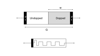
Fig.1 illustrate the generic structure of memristive devices. The memristor can be considered as two regions in series, doped and undoped. Ideally, the resistance difference between doped and undoped region is very high and the overall device resistance is a function of doping ratio(w/G), where w the length of the doped region, and is the thickness of the memristor. The size of these regions can be changed depending on amount and direction of the charge that flow through the device. For instance in a voltage-controlled, by applying a positive voltage increases the thickness of doped region increases until , and the resistance will be very low or device is in ON state.deally, memristors can be programmed to represent analog memory or various intermediate resistance states between HRS and LRS [37]. Because of their programmable resistive states and small footprint (in order of a few nm), memristors are promising candidates for efficiently implementing the synaptic connection between pre-synaptic and post-synaptic neurons. There has been significant activity dedicated to developing memristive-based neuromorphic systems [40, 38, 39, 30]. A variety of oxide-based materials (e.g. ,, , , , ) have been investigated to implement the synaptic array in neuromorphic systems [45, 46, 31], for applications such as pattern recognition [42], face detection [43], learning algorithms [44]. Further details on memristive synapse implementations is beyond the scope of this paper. However readers can refer to Hong et al. [31] for a comprehensive survey of oxide-based memristor devices and their benchmarking metrics for neuromorphic computation.
Crossbar-based structures are typically used to implement synaptic arrays. In crossbar schemes, the memristors are placed on the cross-point between vertical and horizontal wires. However by increasing the size of crossbar array the power consumption dramatically increases. This happens due to sneak current path of memristive-based memory elements as well as other alternate current path. It is therefore memristors are typically placed on the grid point in series with an access transistor to limit the sneak current. Also referred to as 1T1R (one-transistor-one-resistor), such scheme leads to larger cell size e.g. , and lowers the memory density. 1D1R (one-diode-one-resistor) and 0T1R [41] are among other solutions that have been investigated for limiting the sneak current issues [47].
Hybrid CMOS-memristor based architectures have been proposed based on the cross-net structure [48], where the idea has been to use a grid of synaptic memristive devices on the top of CMOS implemented neuronal arrays (see fig. 2). Successful implementations of such a scheme can help to significantly scale the number neurons and synapses on a single die compared to standard CMOS technology. The memristor devices have also been utilized to implement training algorithms, for instance back-propagation [49] and biologically-inspired learning rules e.g. Spiking-timing Dependent Plasticity (STDP). Furthermore, the potential of all-memristive neuromorphic computing system has also been examined [50]. CBRAM [51, 52] and oxRAM [53] are examples of other nanoscale devices that have been studied for implementing synapse circuits. Their structure is based on Metal-Insulator-Metal (MIM) configuration, and are typically used as binary memory elements. While it is possible to program these devices with multi-bit resolutions, it is often achieved at the cost of a higher variability and larger control circuits [54]. These devices are typically fabricated using different materials and techniques [35], and therefore, depending on configuration, represent different electrical characteristics.
Although the efficiency of memristor devices has been successfully demonstrated for single device or a small array of synapses [38], the potential of large-scale CMOS-memristor based design are still being explored in academia. The device reliability, manufacturability, and yield issues are major obstacles in implementing a large synaptic matrix based on the emergent nanoscale memories. Combinations of different switching materials are being investigated in order to overcome these limitations in large-scale integrations of neuromorphic CMOS and memristors. If successful, it would further reduce the power requirements for performing computation. In the next section, we discuss the communication requirements of next-generation scalable low-power neuromorphic processors, and investigate the impact of communication and computation in overall power consumption.
3 Communication requirements
A diverse variety of spike-based neuromorphic computing systems have been developed and implemented in silicon over the past three decades. There are many differences in the implementation details of each system, based on the goals of the implementation and the state of silicon technology at the time the system was created. For instance early implementations were dominated by analog circuit design, but completely or mostly digital implementations can be seen in recent years due to the scaling of CMOS device technology from a feature size of 3m in the mid 1980s to 14nm and below today. Some systems aimed to faithfully mimic Biology—which included operating at Biological time constants. Others were aimed at accelerated modeling, with time constants many orders of magnitude faster than Biology. These choices have cascading implications that change the overall architecture of the neuromorphic system. In particular, communication requirements can change dramatically depending on the implementation goals.
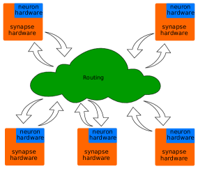
Despite their many differences, neuromorphic systems all attempt to emulate Biology. This means that no matter how various aspects of Biology are modeled, the hardware representing neurons and synapses must logically operate in a massively parallel fashion. Hence, it is possible to view every large-scale neuromorphic hardware platform as a parallel collection of neurons and synapses with some communication infrastructure. Furthermore, it is widely accepted that neurons and synapses have dense local connectivity and relatively sparse global connectivity. Hence, every platform consists of a collection of clusters of neurons and synapses that support efficient local communication within the cluster combined with a global inter-cluster communication network (Fig. 3).
The flexibility of a routing architecture determines the connectivity between neurons and synapses that is natively supported by the hardware. It should come as no surprise that there is a high cost to be paid for supporting highly flexible connectivity, whereas systems that are more restrictive can be made more efficient. The cost of flexibility is higher design complexity and more hardware resources including on-chip memory. In this section, we examine the communication requirements for a generic spiking neural network and possible trade-offs between the system flexibility and its complexity.
Consider a system that models neurons and synapses per neuron. ( for the mammalian brain, and .) Since the average number of incoming connections to a neuron from other neurons is , it follows that the average outgoing connections from a neuron is also (with some exceptions for external inputs and outputs). A neuromorphic communication network has to support an average fan-out of roughly in silicon. Static usage of wiring resources for this purpose is infeasible, since VLSI systems have always been wiring limited even when the average signal fanout is in the range of three to four destinations. Therefore, packet switching is the architecture of choice for global communication in neuromorphic systems. The speed of silicon device switching is used to time-multiplex wires to provide support for global communication. The address-event representation (AER) is most commonly used communication protocol in neuromorphic systems. In the AER protocol, each neuron is given a unique address and upon generating a spike, the addresses packet is routed to the destinations of the source neuron. Hence, the global inter-cluster communication network is a packet-switched communication network, and its single-chip component is a network-on-a-chip (NoC).
3.1 Routing memory
Assume a generic spiking neural network with neurons and synapses per neuron. This results in total destinations. In conventional routing schemes used by parallel machines, each destination would be assigned a unique address encoded with bits. In order to support arbitrary connectivity, bits would have to be stored—which corresponds to GB of storage for a million neuron system (KB per neuron), which would dominate the silicon area needed for the system. Many techniques have been introduced to reduce the storage required. One approach groups the synapses for a neuron by their type e.g. inhibitory vs excitatory, fast vs slow, etc. Modeling the computation performed by the synapse as a linear filter permits the per-synapse state to be grouped by synapse type using the principle of superposition [23]. If there are types of synapses, the storage requirements would be . However, even for small (e.g. ), this only reduces the storage by a factor of . For this reason, state of the art neuromorphic systems typically limit the flexibility of supported connectivity in order to limit the memory needed to store connectivity information.
3.2 Latency constraints
In neuromorphic hardware systems, spikes are represented by binary addresses sent in the form of packets across the network. The packets carry the spikes’ timing (implicitly) and contain the routing information to create the virtual connection(s) between a source node and its destination(s). The packets may include other information such as axonal delays or synaptic weights. In terms of the size, the spike packets in neuromorphic hardware are typically smaller of those of conventional communication networks, consisting of little more than the packet header that stores routing information. Since neuromorphic systems represent information in the timing of spikes, it is important that the communication network preserve the delivery time of a spike relative to the time it was generated. In other words, the communication network must have predictable latency relative to the time scale of the computation. In what follows, we assume a packet switched network consisting of a collection of routers interconnected in some pre-defined topology [24].
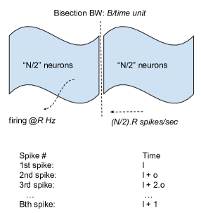
The bandwidth and timing requirements are the important factors in the design of large-scale neuromorphic hardware systems. Fig. 4 illustrates a sketch of network with neurons with firing rate of ( is typically Hz). Consider a very simple network model, where the network has a bisection bandwidth spikes/s, spike latency of , and mean router link occupancy per spike of . Since the bandwidth of a link is determined by the rate at which it can process spikes, the link bandwidth is spikes/s. Such a network requires fraction of time unit to route the first spike, for the second spike and so on for spikes sharing a link. The number of links between the two halves of the network in Fig. 4 will be . If all neurons in one half of the network generate spikes in a synchronized fashion, and the spikes have to be delivered to the other half, the network can support the traffic if . However, the number of links and not just the bandwidth matters since that impacts the packet latency. Since there are links, even under uniform distribution of traffic, the last group of packets will have a latency of while the first set of packets will have a latency of . Hence, the uncertainty in spike arrival will be in the range of relative to when the spikes were generated. Note that for a fixed bisection bandwidth, it is better to have more parallel links (higher ) with lower bandwidth per link if the traffic can be distributed across them. (Note that the Biological extreme of dedicated wiring minimizes this quantity, but is infeasible in current silicon technology.)
For a firing rate of Hz, Biological models typically care about temporal precision in the ms range [25] (i.e. ). Using this rule of thumb to bound the timing uncertainty, we have that , i.e. —a significantly stricter requirement than for conventional networks where the packet timing does not carry information. For accelerated network modeling (i.e. values of significantly faster than real-time), there is “double penalty” for the speedup: one from simply a larger volume of traffic, and a second from a much stricter latency delivery constraint. For and Hz, even with links between two halves of the network, this comes to Gspikes/s rather than Mspikes/s for traditional networks. Note that both numbers scale down once we assume significant communication locality, i.e. if we assume that rather than neurons generate spikes that have to cross over to the other half of the network. Also, the bandwidth requirement can be reduced by relaxing the temporal precision used by the system—going from a ms tolerance to a ms tolerance would cut the bandwidth requirement by a factor of ten. This is why most state-of-the-art neuromorphic systems have networks that at first glance look highly over-designed and underutilized—the latency constraint compounds the network bandwidth requirement.
3.3 Topology and router design
The NoC architecture is specified by its topology and routing strategy. Different topologies have been adopted to support higher throughput demands over time. One-dimensional, two-dimensional, and hierarchical networks are examples of NoC topologies that are utilized by the neuromorphic community. The link bandwidth between routers in a NoC can also be estimated using an analysis similar to the one above. Assuming that a cluster of neurons has on average neurons that have to communicate with neurons in a different cluster, if is the average degree of a router and the average number of links traversed by a spike is , then each link will have to support traffic that is approximately . Using an argument similar to the one above, the latency uncertainty of a link is , where is the link bandwidth. Hence, the link bandwidth requirement is . An analysis without latency constraints would result in . Hence, the network has to be designed to support much higher per link bandwidth to preserve spike timing, even though only a small fraction of the bandwidth is utilized in practice.
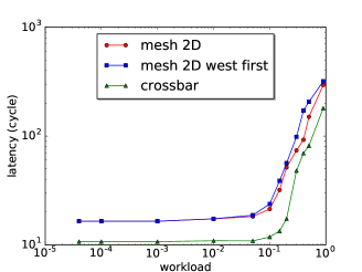
A major difference between the neuromorphic and conventional NoCs is the amount of network traffic generated by a node in the network. In contrast to conventional applications of NoCs, the computing nodes (neurons) in neuromorphic systems run at very low frequencies (in order of Hz), and so drastically lower traffic is injected into the routing fabric. Fig. 5(a) shows the average latency for different networks with high workloads as simulated by a NoC simulator used for computer architecture studies [28]. As the figure suggests, the latency in the networks with high workload varies significantly by network topology and routing algorithm in addition to the network load. However, as we have argued above, the link bandwidth has to be over-provisioned relative to conventional networks in order to keep the spike delivery uncertainty small. Hence, as far as the network is concerned, we are operating in a regime with very low workload compared to the peak feasible bandwidth. As can be seen (Fig. 5(a)), in networks with very low workload (below 0.01 spike/neuron/cycle), the routing methodology and the network load does not significantly impact the network latency. Given the cycle time of NoC digital circuits (at most a few nanoseconds) and the low neuronal firing rates (in order of a few Hz), most neuromorphic NoC workloads fall well below 0.001 spikes/neuron/cycle. This characteristic means that the network topology and routing algorithm is not as important in systems operating at Biological time scales compared to conventional NoCs.
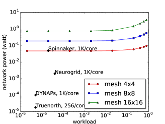
Another differentiating feature is that the power consumption of a neuromorphic core is usually substantially lower than that of conventional compute cores like microprocessors that are traditionally used with NoC fabrics. For example, in both the TrueNorth [13] and DYNAPs [26] projects, the neural cores are custom designed and require a fraction of the power consumption of a standard low power microprocessor. So, for neuromorphic systems, the power consumption of the routing fabric can be a significant portion of the total system power. Fig. 5(b) shows the estimated network power used by an architectural NoC simulator [27] that is used to study on-chip networks. Apart from the SpiNNaker project (which consists of a large number of ARM cores as compute nodes), other neuromorphic systems have networks that consume orders of magnitude less power than those modeled by the NoC simulator because they are much more parsimonious in their hardware usage. We note that the estimated power of different neuromorphic networks in Fig. 5(b) are not intended for direct comparison with each other, as they represent different choices in terms of network flexibility; we simply note that reducing the network power consumption is an important aspect of neuromorphic hardware design. In the light of new memory technologies, the power gap between the computation and communication in custom-designed neuromorphic systems is likely to increase, making the network power consumption even more important in future neuromorphic systems.
3.4 Existing Large-scale Neuromorphic CMOS Architectures
We briefly review major existing neuromorphic hardware systems and their design choices in addressing the design scalability challenges. As will be evident, each system is organized as a cluster of neurons and synapses with a global inter-cluster communication network. Table 1 shows examples of representative neuromorphic hardware systems that have been developed by academic and industrial research teams.
The system architecture developed during the SyNAPSE project, called TrueNorth [13], is the largest single chip built within the neuromorphic community with 1 million neurons, 256 million synapses, and a network of 4096 neurosynaptic cores. Each core contains 256 neurons and 256256 synapses using SRAM-based cross-bar arrays. The neurons and synapses implemented in the “neurosynaptic core” are designed to have behavior that matches a deterministic software model for the system. The global routing topology is a two-dimensional mesh architecture. Thanks to the power efficiency of asynchronous circuits and the use of low-leakage CMOS process, the power figure reported for TrueNorth is its most distinguishable feature compared to other neuromorphic hardware efforts. The chip consumes only 72 mW—significantly lower than other neuromorphic substrates [13].
The Loihi chip [17], designed by Intel, is a many core neuromorphic architecture that comprises 128 neural cores, three embedded x86 processors and asynchronous 2D mesh network-on-chip routing fabric for connecting the neural cores. Each neuromorphic core is equipped with a programmable learning engine to implement different training algorithms. The learning capability and more flexible routing network distinguish Loihi from prior large-scale custom-designed neuromorphic systems. The communication architecture is also mesh based. Loihi is a fully digital architecture implemented in 14 nm CMOS process, and its routing network is designed using asynchronous circuits.
The Neurogrid project consists of a system that comprises almost entirely of custom mixed-signal hardware for modeling biological neurons and synapses. The core hardware element in Neurogrid is the Neurocore chip, which is a custom ASIC that uses analog VLSI to implement neurons and synapses, and digital asynchronous VLSI to implement spike-based communication. The chip was fabricated in a 180nm process technology, and contains a 256256 array of neurons whose core functionality is implemented with analog circuits. Each neuron is implemented using custom analog circuitry that directly implements a a quadratic integrate-and-fire (QIF) model, and is combined with four types of synapse circuits [20]. The routing architecture uses a tree topology, with hardware support for multicasting.
| Truenorth [13] | Spinnaker [14] | Neurogrid [20] | Loihi [17] | |
|---|---|---|---|---|
| Solution | Chip | Board | Board | Chip |
| Technology | 28 nm | 130 nm | 180 nm | 14 nm |
| Comput. core | custom-digital | Commercial-digital | Custom-Mixed | Custom-digital |
| Processing type | Time multiplexing | Time multiplexing | Parallel | Parallel |
| No. of neurons | 1 M | 846 K | 1 M | 131 K |
| On-chip Learning | No | Yes | No | Yes |
| Power consumption | 72 mW | 75 W | 3 W | – |
| Computation power | 30 | 52 | – | – |
| Communication Power | 10 | 12 | – | – |
| Static Power | 60 | 36 | – | – |
The SpiNNaker (Spiking Neural Network Architecture) project [14] at the University of Manchester has taken the most “general-purpose” approach to the design of large-scale neuromorphic systems. The core hardware element for the neuromorphic system is a custom-designed ASIC called the SpiNNaker chip. This chip includes eighteen ARM processor nodes (the ARM968 core available from ARM Ltd, one of the project’s industrial partners), and a specially designed router for communication between SpiNNaker chips [29]. The routing topology is a two-dimensional torus, with additional diagonal connections. A complete SpiNNaker board contains 47 of these chips, and the goal is to assemble 1200 of these boards. A full SpiNNaker system of this size would consume about 90 KW.
3.5 Summary
When examining a complete neuromorphic system, a few items become quite clear. First, the static power consumption is a large fraction of the total power budget. This is because neuromorphic systems operate at very slow timescales compared to the capabilities of modern CMOS devices. The traditional approach taken by conventional digital systems—namely running computation at a very high throughput, which amortizes the static power consumption—is not as easy to accomplish in the neuromorphic domain due to the “double penalty” imposed by strict latency constraints. Note that while our analytical modeling is quite simple, its simplicity is what makes it applicable to a large class of neuromormophic systems. Second, traditional on-chip network architectures consume significantly more power than the custom-designed networks in neuromorphic chips. In spite of this, the network power is a double-digit percentage of the total system power. This means that even if the rest of the system took zero power, the maximum power benefit would be limited by a factor of ten. Finally, the approach of using a large number of small clusters to achieve power efficiency means that any memory requirements for routing have to be distributed into a large number of small memories rather than a single monolithic memory. Hence, what becomes important is not how large a single memory bit is, but the effective density of a small memory array. The array efficiency of a memory array is the ratio of the area occupied by the storage elements (the bits) to the total area of the memory—which includes addressing as well as read/write circuitry. Even SRAMs (which arguably have the simplest external circuitry while having the largest storage element area) have array efficiencies as low as 50%-80% for sizes below 1Mb. A smaller storage element proposed by numerous researchers makes the array efficiency even worse when the memory size is fixed. This observation was validated in a design that used phase-change memory technology as the synaptic element [55].
4 Less explored device technologies for neuromorphic hardware
In this section, we present some less-explored device technologies that have been proposed to improve the performance of memory systems, that also have applicability in improving the scalability of neuromorphic systems.
4.1 Three-dimensional integrated circuits
Three-dimensional (3D) integration has been explored as a way to improve memory system performance by vertical stacking of multiple memory device layers. This technology is mature enough so that it is commercially available, as it has demonstrable advantages in improving integration density of memory with logic. Also, since neuromorphic circuits operate with extremely low power budgets, one of the major concerns in 3D integration—the problem of heat dissipation—is alleviated.
Neuromorphic networks are typically composed of a massively parallel collection of neurons and synapses with large neuronal fan-outs. A vast majority of hardware resources in neuromorphic systems are therefore dedicated to the interconnections between the computing modules. Unlike biology, neuromorphic VLSI systems are implemented in 2D substrates. The large number of connections imposes serious design challenges for scaling up the size of neuromorphic networks in VLSI. Recent advances in semiconductor industry e.g. flip-chip and Through-silicon-vias (TSV) offer vertical integrations of integrated circuits. Such integrations potentially would lead to significant performance improvements in implementing highly interconnected networks, in comparison to their planar counterparts. TSV technology [57, 58] is one of the most promising solutions for stacking of multiple dies in a small package and for memory integration with conventional CMOS. 3D TSV-based ICs are used in stacked memory and processing systems [59, 60], CMOS&MEMS image sensors [62], IoT Socs [63], and 3D FPGAs [64]. Utilizing TSV in vertical integrations reduces wire complexity, the 2D die size, and the interconnection delays in high density interconnect networks. However, such integrations face serious technological challenges from design and physical stand point. A major drawback in design of 3D TSV ICs is the lack of commercial EDA tool support, and accurate electrical models that could capture the physical properties of the TSV connections integrated with CMOS circuits [61]. IC design tools equipped with detailed TSV characterization models can greatly help in investigating the full potential of this technology across different application domains. Depending on operating frequency, TSV links can have resistive or capacitive behavior. A detailed model and frequency response of TSV channels are presented in [56]. Thermal power and cross-talk issues are other important factors to be considered in utilizing TSV connections with CMOS. Furthermore, TSV arrays may impact the behavior of CMOS-based circuits by inducing thermo-mechanical stress in the front end of line (FEOL) layer [58].
Three-dimensional TSV integration technology can enable a higher level of parallelism in highly-interconnected neuromorphic computing networks, with layered structures [65]. In such configuration, each layer contains one or multiple neural modules and TSV arrays represent inter-module connections. Given the huge number of inter-neuron connections, it is impractical to utilizes one TSV link per each neural connection, mainly because of TSV-to-TSV coupling [66], crosstalk [57], and density issues [65]. TSV technology offers opportunities for energy/performance improvements in large-scale neuromorphic design by reducing the network distance per spike (parameter in the analysis presented in section. 3) by having a higher radix router. Energy cost of communication networks is directly a function of the number of hops (routers and interconnects) that neural spikes traverse from source to the destinations. Therefore, TSV-based neuromorphic systems are expected to offer better energy cost compared to 2D structures. It is noted that the router’s complexity in TSV-equipped hypercube neuromorphic designs increases due to extra links required per inter-layer router. In order to investigate the feasibility and impact of TSV technology on large-scale neuromorphic designs, it is paramount to have access to more detailed TSV models and design tools.

4.2 Nano-Electro-Mechanical Systems (NEMS)
Nano-electro-mechanical systems are miniaturized mechanical systems that use the mechanical properties of silicon (and other materials) in addition to the electronic properties to build circuits. NEMS has also been proposed as a way to reduce leakage currents in CMOS, and hence could benefit neuromorphic systems where leakage power dominates.
Excessive leakage current of field-effect transistors is a major obstacle in design of neuromorphic circuits in ultra deep sub-threshold CMOS processes [69, 68]. Device’s off-current consume power even when the transistors are inactive. The problem aggravates in advanced CMOS processes e.g. 28 nm where the off-current is in-negligible in comparison to on-current of the transistors, leading to an increase in total power dissipation. The power breakdown presented in Table 1 shows that the static power consumption becomes a dominant factor of total power dissipation in large-scale custom neuromorphic systems, especially once computation power is reduced using emerging devices. For instance, the static power in TrueNorth [13], a fully-digital design, accounts for 60% of total power, at 20 HZ firing rate. The power leakage issue in deep-submicron mixed-signal neuromorphic designs would be even more critical than digital designs [68]. Mixed-signal design typically occupy larger silicon area (higher static power), due to their highly parallel structure. In addition, the leakage current may impact the behavior of analog sub-threshold circuit blocks. The neuromorphic sub-threshold CMOS neuron and synapse circuits typically operate within pico-ampere currents, while off-current of NMOS transistors in 28 nm can be as high as pico amperes (Fig. 6), even for long transistors (e.g. Length=300 nm), are integrated with digital switches. In other words, larger leakage current not only leads to higher power dissipations, but also narrows down the range of currents in which the neuromorphic sub-threshold circuits can reliably operate.
Nano electro-mechanical (NEM) switches have been recently been investigated as a potential alternative to CMOS [69, 70, 71, 72, 73]. The potential of NEM devices have been investigated for SRAM cells [74, 70, 75], FPGAs [76, 77], 3D integration [78], asynchronous logic [67], etc. Hybrid CMOS-NEMS neuromorphic circuits, presented in [69], implement the leaky-integrate-fire (LIF) neuron model [79] and take a step toward reducing the leakage power in a neuromorphic system. Normally-open and normally-closed NEM relays can be used to build replacements for NMOS and PMOS switches. A challenge with the ideal scenario depicted here is that manufacturing uncertainty can require different body voltages for different NEMS devices. Compared to digital CMOS switches, the switching delay of NEMS is high, and the number of time a device switches is limited before it fails. However, since neuromorphic systems operating on Biological time scales have extremely low activity, the reliability of NEM switches may not be as important a factor in this application domain compared to high-speed digital logic.
In addition to the neural computation circuits, the NEMS switches can be utilized in local communication blocks in order to alleviate the leakage power issues. Most custom-designed neuromorphic CMOS designs, discussed in Sec. 3.4, have utilized SRAM-based crossbar arrays to implement local connectivity. The SRAM blocks are typically designed using conventional 6-transistor circuits and suffer from high-leakage power consumptions. Within this context, future research works may focus on investigating the potential of NEMS switches in combination with CMOS, for optimally implementing local synaptic connections, as an alternative to high-leakage SRAM cells in large-scale neuromorphic designs.
5 Discussion and Conclusion
In recent years, research interests in exploring the potential of emergent nanoscale device technologies have been growing, as researchers have investigated their application to design more efficient memory and interconnections technologies. Large-scale neural networks are one of many applications that can significantly benefit from reliable emergent memory technologies. A large number of research articles have explored the potential of utilizing new memory devices e.g. memristors, to replace CMOS-based memories in implementing neuromorphic computing units e.g. synapses. The yield, scalability (e.g. size and control overhead), and reliability issues are major obstacles in utilizing the emergent nanoscale devices with current technologies. Although large-scale neuromorphic hardware requires a considerable amount of storage in total, the storage is not centralized; rather, it consists of a large number of small blocks (e.g. [13]) that is distributed with the clusters of neurons and synapses. Hence, the control overhead of accessing a small memory block is non-trivial, so emerging memory technologies do not provide a means to tackle this issue unless they can also reduce this overhead. In order to efficiently utilize the emergent memory technologies in scalable neuromorphic systems, compact and power-efficient small memories are needed.
Successful utilization of the emergent memories in large-scale neuromorphic designs is expected to further reduces power requirements for performing computation. Despite such potential improvement, the impact on total power consumption is debatable. In the recent neuromorphic developments, the power required for computation is not the dominant factor of the total power figure. Static power and communication power are a major fraction of total system power in large-scale designs. Although the emergent memory devices partially help to reduce the static power by replacing high-leakage SRAM blocks, the communication power requirements would remain a major issue.
Emergent 3-D integration technologies such as TSV offer promising solutions to overcome the limitations facing current interconnection technology. TSV-based designs have been explored for variety of systems such as image sensors, memories, FPGAs and SoCs. The 3-D integration technologies have significant potential for highly-interconnected large neuromorphic networks by stacking multiple dies and reducing wire-complexity. Currently this technology is not easily accessible to designers, but this can change with time.
Because of their near-zero leakage current, CMOS-compatible NEMS devices could alleviate the static power issues in CMOS circuit implementations. Hybrid CMOS-NEMS designs have been investigated for memories, FPGAs and 3D SoCs. These switches can be potentially be utilized in communication fabrics in neuromorphic networks.
In this paper, we elaborated on the communication requirements of large-scale neuromorphic designs in terms of power and bandwidth requirements, provided a detailed comparison with conventional network-on-chip architecture, and discussed the potential improvements and issues in integrating the emergent nanoscale technologies in large-scale hardware neural networks. Research advances in emergent memory technologies can offer a route toward improved biological-scale neural computing systems only if they address communication and idle power requirements in addition to the computational requirements of such systems.
References
References
- [1] C. Mead, “Neuromorphic electronic systems” Proceedings of the IEEE, vol.78, no.10. pp. 1629-1636. 1990.
- [2] C.A. Mead and T. Delbruck, “Scanners for visualizing activity of analog VLSI circuitry” Analog Integrated Circuits and Signal Processing. vol. 1, pp 93-106, 1991.
- [3] M. Mahowald and C. Mead, “A Silicon Model of Early Visual Processing,” Neural Networks, vol. 1, pp. 91−97, 1988
- [4] T. Delbruck, “Silicon retina with Correlation-Based, Velocity-Tuned Pixel” IEEE Transactions on Neural Networks, Vol. 4, No. 3, pp. 529-541. 1993.
- [5] R. F. Lyon and C. A. Mead, “An analog electronic cochlea” IEEE Trans. Acoust. Speech Signal Process., vol. 36, no. 7, pp. 1119–1134, 1988.
- [6] Park, Paul KJ, et al. “Computationally efficient, real-time motion recognition based on bio-inspired visual and cognitive processing” in proceedings IEEE International Conference on Image Processing (ICIP), 2015.
- [7] W. S. McCulloch and W. Pitts, “A logical calculus of the ideas immanent in nervous activity Bull” Math. Biophys. 5 115–33. 1943.
- [8] H. N. Mhaskar, and C. A. Micchelli. “How to choose an activation function” Advances in Neural Information Processing Systems. 1994.
- [9] The NEURON Simulation Environment, http://www.neuron.yale.edu/
- [10] The Brian spiking neural network simulator, http://briansimulator.org/
- [11] PyNN - NeuralEnsemble, http://neuralensemble.org/PyNN/
- [12] Blue Brain Project, https://bluebrain.epfl.ch/
- [13] P. A. Merolla, J. V. Arthur, R. Alvarez-Icaza, A. S. Cassidy, J. Sawada, F. Akopyan, B. L. Jackson, N. Imam, C. Guo, Y. Nakamura, B. Brezzo, I. Vo, S. K. Esser, R. Appuswamy, B. Taba, A. Amir, M. D. Flickner, W. P. Risk, R. Manohar, and D. S. Modha, “A million spiking-neuron integrated circuit with a scalable communication network and interface” Science, vol. 345, no. 6197, pp. 668–673, Aug 2014.
- [14] S. Furber, F. Galluppi, S. Temple, and L. Plana, “The SpiNNaker project” Proceedings of the IEEE, vol. 102, no. 5, pp. 652–665, May 2014.
- [15] J. Park, T. Yu, S. Joshi, C. Maier, and G. Cauwenberghs, “Hierarchical address event routing for reconfigurable large-scale neuromorphic systems” IEEE Transactions on Neural Networks and Learning Systems, pp. 1–15, 2016.
- [16] R Serrano-Gotarredona, et al., “CAVIAR: A 45k neuron, 5M synapse, 12G connects/s AER hardware sensory–processing–learning–actuating system for high-speed visual object recognition and tracking”, in IEEE Transactions on Neural Networks, 2009.
- [17] M. Davies et al.,“Loihi: A Neuromorphic Manycore Processor with On-Chip Learning” in IEEE Micro vol. 38, no. 1, pp. 82-99, January/February 2018.
- [18] S. Moradi and G. Indiveri, “A VLSI network of spiking neurons with an asynchronous static random access memory” in IEEE Conference on Biomedical Circuits and Systems. pp. 277–280. San Diego, CA, 2011.
- [19] S. Moradi and G. Indiveri, “An event-based neural network architecture with an asynchronous programmable synaptic memory” IEEE Transactions on Biomedical Circuits and Systems,, vol. 8, no. 1, pp. 98–107, February 2014.
- [20] B. V. Benjamin, P. Gao, E. McQuinn, S. Choudhary, A. R. Chandrasekaran, J. Bussat, R. Alvarez-Icaza, J. Arthur, P. Merolla, and K. Boahen, “Neurogrid: A mixed-analog-digital multichip system for large-scale neural simulations” Proceedings of the IEEE, vol. 102, no. 5, pp.699–716, 2014.
- [21] M. Rahimi, S. Moradi, D. Fasnach, M Ozdas, and G. Indiveri “Programmable spike-timing-dependent plasticity learning circuits in neuromorphic VLSI architectures” in ACM Journal on Emerging Technologies in Computing Systems (JETC) 12.2 2015.
- [22] Yuan Xie, “Emerging Memory Technologies: Design, Architecture, and Applications”, Springer, 2013.
- [23] T. Yu, S. Joshi, V. Rangan, and G. Cauwenberghs, “Subthreshold MOS dynamic translinear neural and synaptic conductance” Int. IEEE/EMBS Conf. Neural Eng., pp. 68-71, 2011.
- [24] William Dally and Brian Towles. “Principles and Practices of Interconnection Networks” ISBN:0122007514, Morgan Kaufmann Publishers Inc., 2003.
- [25] M. Galarreta1 and S. Hestrin, “Spike Transmission and Synchrony Detection in Networks of GABAergic Interneurons”, Science, vol. 292, Issue 5525, pp. 2295-2299, 2001.
- [26] S. Moradi, N. Qiao, F. Stefanini and G. Indiveri, “A Scalable Multicore Architecture With Heterogeneous Memory Structures for Dynamic Neuromorphic Asynchronous Processors (DYNAPs)” IEEE Transactions on Biomedical Circuits and Systems, vol. 12, no. 1, pp. 106-122, 2018. doi: 10.1109/TBCAS.2017.2759700
- [27] C. Sun et al.,“DSENT - A Tool Connecting Emerging Photonics with Electronics for Opto-Electronic Networks-on-Chip Modeling” IEEE/ACM Sixth International Symposium on Networks-on-Chip, Copenhagen, 2012, pp. 201-210.
- [28] N. Agarwal, T. Krishna, L. S. Peh and N. K. Jha, “GARNET: A detailed on-chip network model inside a full-system simulator” IEEE International Symposium on Performance Analysis of Systems and Software, Boston, MA, 2009, pp. 33-42.
- [29] E. Painkras et al.,“SpiNNaker: A multi-core System-on-Chip for massively-parallel neural net simulation” Proceedings of the IEEE 2012 Custom Integrated Circuits Conference, San Jose, CA, 2012.
- [30] G. Indiveri, et al. “Integration of nanoscale memristor synapses in neuromorphic computing architectures.” Nanotechnology, vol.24, no.38, IOP Publishing Ltd, 2013.
- [31] X. Hong ,et al. Oxide-based RRAM materials for neuromorphic computing, in Journal Material Science (2018) 53: 8720.
- [32] S. Yu, D. Kuzum and H. S. P. Wong, “Design considerations of synaptic device for neuromorphic computing” IEEE International Symposium on Circuits and Systems (ISCAS), Melbourne VIC, 2014, pp. 1062-1065.
- [33] L. Chua,“Memristor-The missing circuit element” in IEEE Transactions on Circuit Theory, vol. 18, no. 5, pp. 507-519, September 1971.
- [34] weblink: http://www.hpl.hp.com/news/2008/apr-jun/memristor.html
- [35] L. Zheng, S. Shin and S. M. S. Kang, “Memristor-based synapses and neurons for neuromorphic computing” 2015 IEEE International Symposium on Circuits and Systems (ISCAS), Lisbon, 2015, pp. 1150-1153.
- [36] W. He, et.al. “Customized binary and multi-level HfO2−x-based memristors tuned by oxidation conditions” Nature Scientific Reports, volume 7, Article number: 10070, 2017.
- [37] Merced-Grafals EJ, Dávila N, Ge N, Williams RS, Strachan JP. “Repeatable, accurate, and high speed multi-level programming of memristor 1T1R arrays for power efficient analog computing applications” in Nanotechnology, IOP Publishing Ltd, 2016.
- [38] M. Hu, H. Li, Y. Chen, Q. Wu, G. S. Rose and R. W. Linderman, “Memristor Crossbar-Based Neuromorphic Computing System: A Case Study” IEEE Transactions on Neural Networks and Learning Systems, vol. 25, no. 10, pp. 1864-1878, Oct. 2014.
- [39] T. Serrano-Gotarredona, T. Masquelier, T. Prodromakis, G. Indiveri and B. Linares-Barranco, “STDP and STDP variations with memristors for spiking neuromorphic learning systems” Frontiers in Neuroscience, vol.7, 2013.
- [40] A. Afifi, A. Ayatollahi, and F. Raissi, “Implementation of biologically plausible spiking neural network models on the memristor crossbar-based CMOS/nano circuits” European Conference on Circuit Theory and Design, ECCTD, IEEE, 2009.
- [41] L. Zhao, et. al, “Constructing Fast and Energy Efficient 1TnR based ReRAM Crossbar Memory”, ISQED 2017.
- [42] M. Khalid and J. Singh,“Memristor Crossbar-Based Pattern Recognition Circuit Using Perceptron Learning Rule” in IEEE International Symposium on Nanoelectronic and Information Systems (iNIS), Gwalior, 2016, pp. 236-239.
- [43] T. Ibrayev, et al. “On-chip face recognition system design with memristive Hierarchical Temporal Memory” in Journal of Intelligent & Fuzzy Systems, 34.3, 2018.
- [44] D. Yu et al. “Multilevel resistive switching characteristics in Ag/SiO2/Pt RRAM devices” in IEEE international conference of electron devices and solid-state circuits, 2011.
- [45] S. Kim, et al. “Analog Synaptic Behavior of a Silicon Nitride Memristor” ACS applied materials & interfaces 9 (46), 40420-40427 (2017);
- [46] C. Hsieh, et al. “A sub-1-volt analog metal oxide memristive-based synaptic device with large conductance change for energy-efficient spike-based computing systems”, Applied Physics Letters 109 (22), 223501 2016.
- [47] Y. Chang et al. “Demonstration of synaptic behaviors and resistive switching characterizations by proton exchange reactions in silicon oxide.” in Scientific Report, 2016.
- [48] O. Turel, and K. Likharev, “Crossnets: possible neuromorphic networks based on nanoscale components” Int. J. Circuit Theory Appl. 31 (1), 37–53.
- [49] R. Hasan and T. M. Taha, “Enabling back propagation training of memristor crossbar neuromorphic processors” 2014 International Joint Conference on Neural Networks (IJCNN), Beijing, 2014, pp. 21-28.
- [50] A. Pantazi, et al. “All-memristive neuromorphic computing with level-tuned neurons.” Nanotechnology, vol.27, no.35, IOP Publishing Ltd, 2016.
- [51] M. Suri et al., “CBRAM devices as binary synapses for low-power stochastic neuromorphic systems: Auditory (Cochlea) and visual (Retina) cognitive processing applications” International Electron Devices Meeting, San Francisco, CA, 2012, pp. 10.3.1-10.3.4.
- [52] Cory Merkel, Dhireesha Kudithipudi, Manan Suri, and Bryant Wysocki. “Stochastic CBRAM-Based Neuromorphic Time Series Prediction System”, J. Emerg. Technol. Comput. Syst. 13, 3, Article 37 (February 2017), 14 pages.
- [53] E. Vianello, et al. “Binary OxRAM/CBRAM Memories for Efficient Implementations of Embedded Neuromorphic Circuits”,Neuro-inspired Computing Using Resistive Synaptic Devices, Springer International Publishing, 2017.
- [54] D. Garbin. “A variability study of PCM and OxRAM technologies for use as synapses in neuromorphic systems” Micro and nanotechnologies/Microelectronics, Université Grenoble Alpes, 2015.
- [55] S. Raoux et al.,“Phase-change random access memory: A scalable technology,” in IBM Journal of Research and Development, vol. 52, no. 4.5, pp. 465-479, July 2008.
- [56] Kim et al., “High-Frequency Scalable Electrical Model and Analysis of a Through Silicon Via (TSV)” in IEEE Transactions on Components, Packaging and Manufacturing Technology, vol. 1, no. 2, pp. 181-195, Feb. 2011.
- [57] G. Van der Plas et al.,“Design issues and considerations for low-cost 3D TSV IC technology” IEEE International Solid-State Circuits Conference - (ISSCC), San Francisco, CA, 2010, pp. 148-149.
- [58] Shen W-W, Chen K-N. “Three-Dimensional Integrated Circuit (3D IC) Key Technology: Through-Silicon Via (TSV)” Nanoscale Research Letters, 2017;12:56.
- [59] D. H. Kim et al.,“Design and Analysis of 3D-MAPS (3D Massively Parallel Processor with Stacked Memory” in IEEE Transactions on Computers, vol. 64, no. 1, pp. 112-125, Jan. 2015.
- [60] H. Saito et al.,“A Chip-Stacked Memory for On-Chip SRAM-Rich SoCs and Processors” in IEEE Journal of Solid-State Circuits, vol. 45, no. 1, pp. 15-22, Jan. 2010.
- [61] M. A. Ehsan, Z. Zhou and Y. Yi, “Electrical modeling and analysis of sidewall roughness of through silicon vias in 3D integration” IEEE International Symposium on Electromagnetic Compatibility (EMC), Raleigh, NC, 2014, pp. 52-56.
- [62] D. Henry et al. “Through silicon vias technology for CMOS image sensors packaging” 58th Electronic Components and Technology Conference, Lake Buena Vista, FL, 2008, pp. 556-562.
- [63] T. T. Wu et al.,“Low-cost and TSV-free monolithic 3D-IC with heterogeneous integration of logic, memory and sensor analogy circuitry for Internet of Things” IEEE International Electron Devices Meeting (IEDM), Washington, DC, 2015, pp. 25.4.1-25.4.4.
- [64] X. Wu,“3D-IC FPGA: KGD, DFT and build-in FA capabilities,” IEEE 22nd International Symposium on the Physical and Failure Analysis of Integrated Circuits, pp. 4-7. 2015.
- [65] H. An, M. A. Ehsan, Z. Zhou and Y. Yi,“Electrical modeling and analysis of 3D Neuromorphic IC with Monolithic Inter-tier Vias” IEEE 25th Conference on Electrical Performance Of Electronic Packaging And Systems (EPEPS), San Diego, CA, 2016, pp. 87-90.
- [66] Z. Yingbo, D. Gang. and Y. Yintang, “Analysis and optimization of TSV–TSV coupling in three-dimensional integrated circuits” Journal of Semiconductors, IOP Publishing Ltd, 2015.
- [67] B. Z. Tang, S. Bhave, and R. Manohar. “Low power asynchronous vlsi with nem relays” In 20th IEEE International Symposium on Asynchronous Circuits and Systems pages 85–92. IEEE, 2014.
- [68] N. Qiao and G. Indiveri, “Scaling mixed-signal neuromorphic processors to 28 nm FD-SOI technologies” 2016 IEEE Biomedical Circuits and Systems Conference (BioCAS), Shanghai, 2016, pp. 552-555.
- [69] S. Moradi, S. A. Bhave and R. Manohar, “Energy-efficient hybrid CMOS-NEMS LIF neuron circuit in 28 nm CMOS process” IEEE Symposium Series on Computational Intelligence, Honolulu, HI, 2017.
- [70] N. Xu et al., “Hybrid CMOS/BEOL-NEMS technology for ultra-low-power IC applications” 2014 IEEE International Electron Devices Meeting, San Francisco, CA, 2014, pp. 28.8.1-28.8.4.
- [71] F. Chen, H. Kam, D. Markovic, T. J. K. Liu, V. Stojanovic and E. Alon, “Integrated circuit design with NEM relays” 2008 IEEE/ACM International Conference on Computer-Aided Design, San Jose, CA, 2008, pp. 750-757.
- [72] D. Kim, D. C. Ahn, M. G. Allen and Y. K. Choi,“Triboelectrification driven fin-fact (flip-flop actuated channel transistor) for security application” 2017 IEEE 30th International Conference on Micro Electro Mechanical Systems, Las Vegas, NV, pp. 171-174, 2017.
- [73] A. Peschot, Q. Chuang, and K. L. Tsu-Jae, “Nanoelectromechanical switches for low-power digital computing” Micromachines, 6.8 (2015): 1046-1065.
- [74] S. choong et.al. “Nanoelectromechanical (NEM) relays integrated with CMOS SRAM for improved stability and low leakage” in Proceedings of the 2009 International Conference on Computer-Aided Design, pp. 478-484. San Jose, CA, 2009.
- [75] S. Xiao, author, D. R Andersen, W. Yang, “Design and Analysis of Nanotube-Based Memory Cells” Nanoscale Res Lett, (2008) 3: 416.
- [76] Y. Zhou, S. Thekkel and S. Bhunia, “Low power FPGA design using hybrid CMOS-NEMS approach” ACM/IEEE International Symposium on Low Power Electronics and Design (ISLPED), pp. 14-19. Portland, OR, 2007.
- [77] S. Han, V. Sirigiri, D. G. Saab and M. Tabib-Azar, “Ultra-low power NEMS FPGA” in IEEE/ACM International Conference on Computer-Aided Design (ICCAD), San Jose, CA, 2012, pp. 533-538.
- [78] X. Huang, C. Zhang, H. Yu and W. Zhang, “A Nanoelectromechanical-Switch-Based Thermal Management for 3-D Integrated Many-Core Memory-Processor System” in IEEE Transactions on Nanotechnology, vol. 11, no. 3, pp. 588-600, May 2012.
- [79] M. Mahowald and R. Douglas, “A silicon neuron” Nature volume 354, pages 515–518, 1991.