Mechanical dissipation from charge and spin transitions
in oxygen deficient SrTiO₃
Abstract
Bodies in relative motion separated by a gap of a few nanometers can experience a tiny friction force. This non-contact dissipation can have various origins and can be successfully measured by a sensitive pendulum atomic force microscope tip oscillating laterally above the surface. Here, we report on the observation of dissipation peaks at selected voltage-dependent tip-surface distances for oxygen-deficient strontium titanate () surface at low temperatures (). The observed dissipation peaks are attributed to tip-induced charge and spin state transitions in quantum-dot-like entities formed by single oxygen vacancies (and clusters thereof, possibly through a collective mechanism) at the surface, which in view of technological and fundamental research relevance of the material opens important avenues for further studies and applications.
Introduction
Strontium titanate ( or for short) stands out among other oxides as a material with broad spectrum of physical phenomena and of functional properties. Throughout the last decades the interest in has increased due to its popularity as a versatile substrate for oxide electronics research and engineering Goodenough2004 ; Marshall2015 . Extreme electron mobility and superconducting properties Ohta2007 ; Santander-Syro2014 ; Taniuchi2016 , quantum paraelectricity in bulk Muller1991 , itinerant, impurity, and vacancy based magnetism Salluzzo2013 ; Liu2013b ; Marshall2015 of have been subjects of fundamental studies. In particular, charge trapping by oxygen vacancies () Shanthi1998 and vacancy related magnetism Lin2010 ; Lin2011a ; Rice2014 ; Brovko2017 are pertinent to the present study. Pristine develops oxygen vacancies when grown or annealed under oxygen-poor conditions Janousch2007 , bombarded with noble gas ions Chang2015 , or under intense laser or ultraviolet irradiation Rao2014 . When in numbers, can lead to the formation of two-dimensional electron gas (2DEG) on the surface of bare Meevasana2011 ; Plumb2014 ; Santander-Syro2011 ; DiCapua2012 . Moreover, oxygen vacancies were shown to be inherently magnetic both in bulk Lin2013a ; Rice2014 ; Zhang2015a and at its surface Cuong2007 ; Alexandrov2009a ; Choi2013 ; Pavlenko2013 ; Lopez-Bezanilla2015 ; Li2015 ; Taniuchi2016 ; Altmeyer2016 ; Brovko2017 . They were shown to exhibit either local uncorrelated magnetic moments Lin2013a ; Garcia-Castro2016 or stable long-range magnetic order, when present in sufficient concentration Liao2012 ; Pavlenko2013 ; Rice2014 ; Rice2014a ; Taniuchi2016 ; Altmeyer2016 ; Trabelsi2016 . Although the influence of bulk and surface oxygen vacancies on the electronic and optical properties of is long known Bannikov2008 ; Liu2015a , the options for controlling these vacancies are poorly explored and offer a lucrative field for further research.
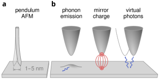
Atomic force microscopy (AFM) cantilevers oscillating like tiny pendula over a surface Kisiel2011 are primarily designed to measure extremely delicate non-contact form of frictional dissipation and serve as an ultra-sensitive, non-invasive spectroscopy method Kisiel2015 (see Supplementary Methods Fig. 1 for details). Apart from provoking such conventional forms of non-contact energy transfer as phonon and Joule ohmic dissipation Volokitin2006 ; Kisiel2011 , the external perturbation caused by an oscillating tip might push a finite quantum system, or a collection of them towards a transition or a level crossing with subsequent relaxation of the system. A level crossing implies a dissipation channel for the external agent provoking the change Cockins2010 ; Kisiel2015 . For AFM this leads to distance and bias-voltage-dependent dissipation of the tip oscillation energy. Such dissipation was observed at the sudden injection of phase slips into a charge density wave on surface Langer2013 and at the crossing of electron energy levels in mesoscopic single-electron quantum dots Cockins2010 .
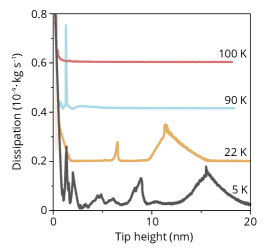
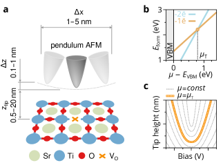
Here we measure the dissipation experienced by a sharp AFM tip oscillating at a range of lateral amplitudes ( to ) over an oxygen deficient single crystal surface cooled down to low temperatures of . At selected tip-surface distances and bias voltages, dissipation peaks are observed in the cantilever oscillation. We attribute these peaks to charge and spin state transitions in individual or possibly collective groups of oxygen vacancies, which act as natural quantum dots at oxygen-deficient surfaces of , as suggested by a recent first principles calculations Brovko2017 . We further discuss possible pathways for electrons which could give rise to these transitions under the action of the time-periodic electrostatic or van der Waals potential exerted by the AFM tip. The dissipation peaks appear at large crystal reduction (therefore with many surface vacancies), and at long tip-sample distances (even above 10 nm), disappearing above . While these elements point to a collective mechanism involving many vacancies, we find that the crude single vacancy model already provides a very helpful level of understanding.
Results
Sample characterization with STM
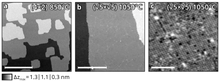
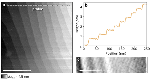
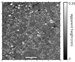
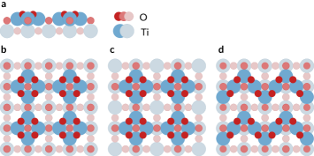
Surface morphology and chemical composition of are known to change significantly under high temperature annealing Dagdeviren2016 . We thus start our study by examining the topography of with a scanning tunneling microscope (STM) between cycles of annealing at subsequently increasing temperatures (see Methods for the measurement protocol and Supplementary Figure 2 for more temperature-dependent measurements). While rough and irregularly-shaped at low annealing temperatures, surfaces develop a well defined terrace and island structure after prolonged annealing at about forming a range of reconstruction patterns [, and dominant c] yet retaining a relatively high surface roughness Tanaka1993 ; Dagdeviren2016 . At about well ordered step-terraces develop and acquire smaller reconstruction unit cells of and arising from oxygen vacancies , a behaviour which persists at higher annealing temperaturesTanaka1993 . Representative constant current topographies after annealing at and are shown in Fig. 1a and Fig. 1b,c, respectively, exhibiting, as mentioned, well formed terraces and roughness at the atomic scale after annealing to and atomically flat terraces with clear reconstruction after Tanaka1993 . The atomic resolution STM image [Fig. 1c] of the -annealed surface with shows several tetragonal reconstruction domains of three different orientations Lemanov2002 . It exhibits a variety of structural peculiarities, which appear as either points or extended areas/lines of increased or decreased apparent height. Bright features can be attributed to adatoms on top of the reconstructed ad-layer or oxygen hydroxyl () groups resulting from rest gases in the vacuum chamber, as it is known Wendt2008 that interstitial atoms can cause a substantial increase in local surface reactivity and thus facilitate group adsorption. Dark features could, on the other hand, indicate missing ad-islands in the reconstruction Shiraki2010 ; Lin2011a or, considering that annealing was carried out at oxygen-poor conditions, more likely represent oxygen vacancies () at or near the surface Setvin2017 ; Tanaka1993 . In agreement with that, the density of empty states 1 eV above Fermi level, which the STM probes, is high at all sites where a surface O atom is present.
Non-contact friction measurements
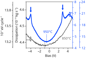
After the topographic characterization of the surface between the annealing cycles we measure the non-contact frictional dissipation coefficient as a function of the applied tip-sample bias voltage. Measurements are taken with a stiff gold-coated tip oscillating in pendulum geometry at a moderate planar amplitude of while kept at a constant tip-sample distance of (see Methods section for details and the definition of and supplementary Fig. 1 for a sketch of the setup). Dissipation spectra for samples annealed at and (see also Supplementary Fig. 3 for morphology characterization) are shown in Fig. 2. Both spectra were taken on flat terraces, far from the step edges. The sample annealed at lower temperature reveals a spectrum which displays a parabolic curve characteristic of Joule non-contact friction Volokitin2006 . Similarity with Nb metal above Kisiel2011 indicates some ohmic electron conduction in the surface. The dissipation spectrum of the annealed sample, however, exhibits in addition two distinct dissipation peaks at located symmetrically around the contact potential voltage and a broader, less pronounced dissipation peak around . Moreover, dissipation spectra obtained with a local probe (metallic tip tuning fork sensor) systematically shown an identical, single dissipation peak for reconstructed after annealing at (see Supplementary Fig. 4). It is the origin of those dissipation peaks, and the physical information on the nanotechnologically important surface oxygen vacancies that the rest of this paper shall be devoted to.
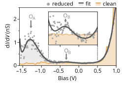
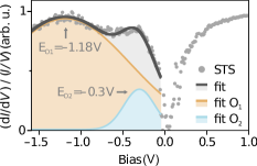
First, we use the scanning tunneling spectroscopy (STS) mode of our AFM to measure at closer tunneling tip-surface distances the spectra (Fig. 3) above the reconstructed areas and above the apparent dark spots in Fig. 1c. The main difference between the spectra of reduced and non-reduced is an additional defect state in the gap ( in Fig. 3) lying at about below the Fermi level, absent for samples annealed at moderate temperatures (for details about the defect state position see Supplementary Fig. 5). Published data Tanaka1993 attribute a similar STS peak to reduced and surface oxygen vacancies, suggesting that the dark STM spots mark vacancies formed in the process of high temperature annealing. Another feature of the differential conductance spectra of is a weaker peak at about below the Fermi level ( in Fig. 3). It can be attributed to a shallower in-gap state of the , which, as shown in our recent theoretical study Brovko2017 can be gradually emptied by changing the local chemical potential of the surface under the scanning probe tip (see Supplementary Fig. 6 for details).
It is therefore natural to assume that the non-contact dissipation peaks (Fig. 2) measured with a AFM tip swinging near the vacancy site should be due to electronic transitions within the vacancy or between the vacancies under the influence of the AFM tip’s potential field changes. In this experiment the large tip-surface distance and its large swing implies that in general more vacancies are likely to be collectively involved in each dissipation event and peak, in a manner that is hard to resolve. The interpretation is greatly helped, we find, by a single vacancy model, as follows. An isolated at the surface of can be regarded as a quantum dot with a discrete set of charge states, a dissipation peak would arise in the tip oscillation from a periodic transition between them. This conclusion may also entrain particularly exciting consequences, as the charge state of an at an surface is uniquely linked to its magnetic state (Brovko2017, ). The dangling bonds of the Ti atoms bordering (see Supplementary Fig. 6 for a sketch) are known to host the two electrons, or fractions thereof, left behind by the departed atom. Calculations show that these electrons occupy dangling bond -localized states corresponding to levels within the band gap of Brovko2017 . Depending on the local value of the electron chemical potential the system can be coerced into an charge-neutral singlet resulting from antiferromagnetically coupled with oppositely aligned spins, the doublet state of a charged single-hole vacancy, and the magnetically dead two-hole () vacancy state Brovko2017 . The local chemical potential in our experiment is controlled by the AFM tip voltage and tip-sample separation. The tip oscillation may thus cause time-periodic transitions of the quantum dot between its different states. A distant tip acts as a pure potential source without any tunneling current, while the vacancy state transition involves a change of charge besides spin. It is necessary, therefore, to understand the physical mechanism by which the charge and spin state transition may be provoked here (see Supplementary Fig. 6).
Local dissipation spectra taken with a stiff cantilever tip
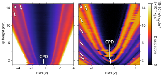
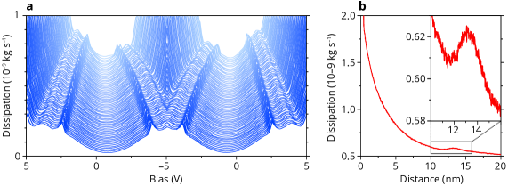
Key clues that clarify the tip-induced transition mechanism are provided by the dependence of the dissipation behavior on the tip-sample distance . For distances spanning a range from near-contact regime to , we measure the bias () dependence of the AFM frictional dissipation coefficient , thus obtaining a full map. We use two different tips in pendulum geometry: (i) a stiffer gold-coated cantilever tip with a moderately low stiffness of operated at a nominal amplitude of and (ii) an ultra-sensitive probe with very low stiffness of () which implies larger oscillation amplitudes of up to . Unlike the stiff cantilever the soft sensor is not gold-coated, which results in a very high value of but requires significant doping of the silicon tips for attaining reasonable conducting properties.
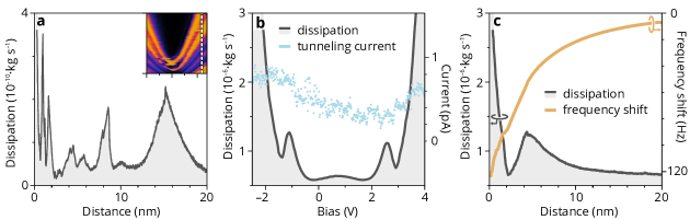
The stiff tip dissipation map taken above a reconstructed section of the surface is shown in Fig. 4a. It shows features found in other similar experiments Kisiel2011 . For each tip-sample distance the friction coefficient exhibits a parabolic behavior (see gray curve in Fig. 2 which is a cross-section of the map in Fig. 4a at ), hallmark of Joule-loss non-contact friction Volokitin2006 ; Kisiel2011 . The map is near-symmetric with respect to the contact potential difference (CPD) voltage marked in the plot. The outer hull of the dissipation map is defined by a the critical bias voltage for excitation of electrons over the band gap of the , signaling a sharp increase in dissipation (about ) at close range. The sharp dissipation peaks at the sub-bandgap voltages marked with arrows both reach , maintaining roughly the same intensity independently of the tip-sample distance. The peaks are observed at non-zero (with respect to CPD) biases even at close range and shift towards higher bias voltages with increasing tip-sample distance, which indicates that the effect is voltage rather than force controlled, similar to the case of quantum dots Cockins2010 and in analogy to quantum dots the amount of dissipated energy given by different sensors is also in the order of 10-20 .
Dissipation spectra taken with a soft cantilever tip
To further investigate the dissipation mechanism we repeat the dissipation measurements with an ultra-sensitive doped-silicon sensor. Very low stiffness () of the sensor implies larger horizontal oscillation amplitudes of up to and the absence of metal coating might imply different interaction behavior. The non-contact friction dependence map taken with a soft tip is shown in Fig. 4b. Here again bright features correspond to the high dissipation maxima up to . However, instead of just two dissipation peaks the soft non-local sensor sports a whole family of dissipation maxima. We noticed a substantial change of CPD value indicated by the elbow shape of the arrow in Fig. 4b in the transition while switching from one to the next dissipation maxima trace. It is consistent with the idea of the oscillating tip causing a persistent accumulation of charge below it and further corroborates the guess that the charging dissipation scenario is responsible for the dissipation peaks. These again proves electronic nature of energy dissipation in analogy to Refs. Cockins2010, ; Cockins2012, .
Discussion
Charge transfer mechanisms
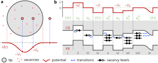
The dissipation peak phenomenology fits a model of charge and spin state transitions in oxygen vacancies present at reduced surfaces, as follows. The distant pendulum tip projects a potential shadow on the underlying (001) surface deforming the local electronic chemical potential (either directly or indirectly by distorting the surface atom positions). This perturbation is larger for a charged tip, but even at zero voltage, the van der Waals polarization interaction shifts the chemical potential by modifying the electron self-energy. If one or more oxygen vacancies happen to lie in the potential shadow of the tip (see Fig. 5a for a sketch) the vacancies closer to the tip’s position experience a different electron chemical potential than those at the periphery. At certain values of the imposed potential (the strength/depth of which is dependent on the tip-sample distance and mutual bias) the topmost filled impurity level of one of the can become aligned with an empty electron reservoir thus provoking one electron to leave the vacancy, causing a transition Brovko2017 . Some of the possible transition paths are sketched in Fig. 5b. Electrons can be exchanged between a neutral vacancy and a charged one, or a vacancy and the conduction band of the surrounding surface as well as the 2DEG known to exist on the doped interfaces of Santander-Syro2011 ; Santander-Syro2014 . Oxygen vacancies on surfaces are known to exist as both isolated entities or as cluster defects. The latter can exhibit multiple impurity levels and reside in a number of charge states Brovko2017 . Alignment of one or several impurity levels of such an extended vacancy with either a single-vacancy impurity level or the electron bath can lead to one or several consecutive electron transitions, taking place by resonant tunneling or generally by electron transfer. An oscillating AFM tip at a fixed bias can cause, when it reaches the right distance, a sufficient deformation of the local chemical potential to provoke one of these transitions, which is reversed as the tip oscillates back. Every single electron transfer channel leading to a transition can manifest itself as AFM tip dissipation peaking precisely when the bias voltage and distance first reach the values required to activate the transfer. The approximately symmetric pattern for positive and negative tip voltage suggests that this mechanism is reversible.
In the dissipation measurements carried out with the stiffer gold-coated tip, the area swept is much smaller, and the two observed dissipation peaks can originate from the single and double discharging of a standalone vacancy with electrons being transferred to either other vacancies/vacancy clusters or to the conduction band. We estimate the average distance between the dark defects on our sample from STM images to be (see Supplementary Fig. 8). Thus a stiff tip swinging with an amplitude of is unlikely to impact more than one vacancy, even considering that the characteristic dimensions of the perturbation caused by the tip suspended at several distance shall be larger than the amplitude of its swing. The softer non-local tip swinging at an amplitude of will, on the contrary, enclose in its potential shadow path several or an cluster resulting in more electron transition channels and consequently more dissipation peaks. The fact that in the latter case some dissipation peaks exist even in the case when the CPD is completely compensated is a likely residual effect of the van der Waals interaction, as the impurity level is a relatively shallow one and does not require much perturbation to be emptied. This assumption is especially important to us since charge states were shown to be stable with respect to mechanical perturbations of the system Brovko2017 thus making the influence of the tip on the observed charge and spin-state transition much more likely to be electronic than mechanical in origin. Unfortunately, we cannot specify exactly what levels we are precisely talking about. Comparison of our STS data with DFT calculations (see Supplementary Fig. 6 and Supplementary Fig. 9; also Ref.Brovko2017 ) suggests that for a single vacancy charging scenario, the observed dissipation might arise from the transitions between q=–2e and q=–1e charge states. Interestingly, that should also involve a spin transition, from of the q=–1e state, to in the q=–2e state, where the two electrons in the two Ti oppositely facing dangling bonds couple antiferromagnetically.Brovko2017 Finally the temperature dependent measurements (see Supplementary Fig. 2) reveal that the dissipation peaks which we attribute to charging and discharging of Oxygen vacancies persist up to a temperature of . At those temperatures the charging energy is much larger than thermal energy () and the occupancy of the can be controlled with single-electron precision, hinting at a wide range of promising functionalities and suggesting that the “shadow potential” projected by the tip works within an energy scale of order . This is not unreasonable, since the vacancy redox levels, all lie very close to the conduction band and can possibly be switched by a tip-induced shift.
We mention, before closing, a work that reported a single noncontact AFM frictional peak on and on NbSe2 Saitoh2010 , as well as theoretical modeling that rationalised it in terms of a defect spin model She2012 . The NbSe2 data show that the peak maximum coincides with the earliest onset of weak tip-surface electron tunneling, and the simultaneous onset of stiffening of the tip frequency. All our AFM dissipation peaks occur at large distances where tunneling is totally absent and where the tip frequency is softened rather than stiffened (see Supplementary Fig. 4). Both elements indicate a dissipation origin different from that of Ref. Saitoh2010, .
To summarize, our sensitive low-temperature () atomic force microscopy experiments with soft cantilever tips show single or multiple mechanical dissipation peaks over a oxygen reduced surface of . We attribute them to the tip coupling to charge and spin state transitions in quantum dots constituted by oxygen vacancies (and clusters thereof). Since for the a charge state transition is intimately coupled to the magnetic properties of the latter, the possibility to study periodically driven transitions in the system also opens up unique avenues to studying the fundamental magnetic phenomena therein. Experimentally it would require operation with a magnetically polarized AFM tip. The presence of surface oxygen vacancies and the ease with which they can give and take electrons must play a role in the technologically important interfaces subsequently formed on this substrate. Caviglia2008 ; Couto2011 .
The electronic characterization provided by the AFM mechanical dissipation peaks reported here may be used as an efficient tool for surface analysis, of considerable nanotechnological importance. For instance, since the the in-gap states of a vacancy or vacancy cluster can be seen as a signature or footprint of the latter and the dissipation map, as is discussed in the present study, is directly dependent on the impurity level alignment, one could use pendulum atomic force microscopy to quickly characterise large areas of a sample with respect to vacancies present thereon.
I Methods
I.1 Tuning Fork Atomic Force Microscopy measurements
The experiments were performed in two independent UHV chambers. The STM/AFM experiments were performed with a commercial qPlus STM/AFM (Omicron Nanotechnology GmbH) running at low temperature () under UHV and operated by a Nanonis Control System from SPECS GmbH. We used a commercial tuning-fork sensor in the qPlus configuration (parameters: resonance frequency , spring constant , quality factor at ). During non-contact friction measurement the oscillation amplitude was always set to . The oscillation frequency and excitation amplitude were recorded simultaneously for different V values applied to the tungsten tip. All STM images were recorded in the constant-current mode. Conductance measurements were performed at constant-height using the lock-in technique with modulation frequency and voltage equal to and , respectively.
I.2 Pendulum AFM energy dissipation measurements
The sensitive non-contact friction experiments were performed under UHV by means of a very soft, highly n-doped silicon cantilever (ATEC-Cont from Nanosensors with resistivity ) with spring constant and stiffer, gold-coated silicon cantilever (ATEC-NcAu from Nanosensors) with spring constant . Both were suspended perpendicularly to the surface and operated in the so-called pendulum geometry, meaning that the tip vibrational motion is parallel to the sample surface Kisiel2011 . Owing to its large stiffness and metallic character, the second tip allowed to perform Scanning tunneling Microscopy (STM) as well as to operate in AFM mode with small oscillation amplitudes allowing for local dissipation measurements. The oscillation amplitudes of the tip were kept constant by means of a phase-locked loop feedback system at for the ultra-sensitive cantilever and at , for the stiff sensor. In AFM voltage dependent measurements the voltage was applied to the sample. The cantilevers were annealed in UHV up to for 12 hours which results in removal of water layers and weakly bound contaminant molecules from both the cantilever and the tip. After annealing the cantilevers quality factors and the frequencies were equal to , and , for soft and stiff probes, respectively. It is also known that this long-term annealing leads to negligible amounts of localised charges on the probing tip.
I.3 Non-contact friction coefficient and energy dissipation
In dissipation measurements the non-contact friction coefficient was calculated according to the standard formula Cleveland1998 :
| (1) |
where and are the distance-dependent excitation amplitude and resonance frequency of the cantilever, and the suffix 0 refers to the free cantilever. The distance corresponds to the point where the tip enters the contact regime, meaning that the cantilever driving signal is saturated and the tunneling current starts to rise. Friction coefficient might be converted into energy dissipation according to the formula:
| (2) |
where is the oscillation amplitude and is elementary charge.
I.4 Sample preparation
The measured sample was 1% doped (001) single crystal which is known to exhibit a variety [, , , , and of surface reconstructions Dagdeviren2016 ; Tanaka1993 if annealed in ultra high vacuum. After few cycles of short-term annealing and Ar sputtering the sample was long term annealed for about 40 min under oxygen deficient conditions, respectively to , and leading to atomically clean surfaces. The temperature of the sample was controlled with a pyrometer. It is known that the process of UHV, high temperature annealing leads to sample oxygen deficiency by creation of surface oxygen vacancies Janousch2007 . After preparation the samples were transferred into the microscope. The AFM and STM measurements were performed at low temperature .
I.5 Data availability
The data that support the findings of this study are available from the corresponding authors upon reasonable request.
References
- (1) Goodenough, J. B. Electronic and ionic transport properties and other physical aspects of perovskites. Reports on Progress in Physics 67, 1915–1993 (2004).
- (2) Marshall, M. S. J., Becerra-Toledo, A. E., Marks, L. D. & Castell, M. R. Defects on Strontium Titanate. In Jupille, J. & Geoff, T. (eds.) Springer Series in Surface Sciences, vol. 58, 327–349 (Springer International Publishing, Switzerland, 2015).
- (3) Ohta, H. et al. Giant thermoelectric Seebeck coefficient of a two-dimensional electron gas in SrTiO3. Nature Materials 6, 129–134 (2007).
- (4) Santander-Syro, A. F. et al. Giant spin splitting of the two-dimensional electron gas at the surface of SrTiO3. Nature materials 13, 1085–90 (2014).
- (5) Taniuchi, T. et al. Imaging of room-temperature ferromagnetic nano-domains at the surface of a non-magnetic oxide. Nature Communications 7, 11781 (2016).
- (6) Müller, K. A., Berlinger, W. & Tosatti, E. Indication for a novel phase in the quantum paraelectric regime of SrTiO3. Zeitschrift für Physik B Condensed Matter 84, 277–283 (1991).
- (7) Salluzzo, M. et al. Origin of Interface Magnetism in BiMnO3/SrTiO3 and LaAlO3/SrTiO3 Heterostructures. Physical Review Letters 111, 087204 (2013).
- (8) Liu, Z. Q. et al. Reversible room-temperature ferromagnetism in Nb-doped SrTiO3 single crystals. Physical Review B 87, 220405 (2013).
- (9) Shanthi, N. & Sarma, D. D. Electronic structure of electron doped SrTiO3 : SrTiO3-δ and Sr1-xLaxTiO3. Physical Review B 57, 2153–2158 (1998).
- (10) Lin, Y.-H., Chen, Y. & Goldman, A. M. Indications of superconductivity at somewhat elevated temperatures in strontium titanate subjected to high electric fields. Physical Review B 82, 172507 (2010).
- (11) Lin, Y. et al. The (2×2) reconstructions on the SrTiO3 (001) surface: A combined scanning tunneling microscopy and density functional theory study. Surface Science 605, L51–L55 (2011).
- (12) Rice, W. D. et al. Persistent optically induced magnetism in oxygen-deficient strontium titanate. Nature Materials 13, 481–487 (2014).
- (13) Brovko, O. O. & Tosatti, E. Controlling the magnetism of oxygen surface vacancies in SrTiO3 through charging. Physical Review Materials 1, 044405 (2017).
- (14) Janousch, M. et al. Role of Oxygen Vacancies in Cr-Doped SrTiO3 for Resistance-Change Memory. Advanced Materials 19, 2232–2235 (2007).
- (15) Chang, J.-W., Lee, J. S., Lee, T. H., Kim, J. & Doh, Y.-j. Controlled formation of high-mobility shallow electron gases in SrTiO3 single crystal. Applied Physics Express 8, 055701 (2015).
- (16) Rao, S. S., Lee, Y. F., Prater, J. T., Smirnov, A. I. & Narayan, J. Laser annealing induced ferromagnetism in SrTiO3 single crystal. Applied Physics Letters 105, 042403 (2014).
- (17) Meevasana, W. et al. Creation and control of a two-dimensional electron liquid at the bare SrTiO3 surface. Nature Materials 10, 114–118 (2011).
- (18) Plumb, N. C. et al. Mixed Dimensionality of Confined Conducting Electrons in the Surface Region of SrTiO3. Physical Review Letters 113, 086801 (2014).
- (19) Santander-Syro, A. F. et al. Two-dimensional electron gas with universal subbands at the surface of SrTiO3. Nature 469, 189–193 (2011).
- (20) Di Capua, R. et al. Observation of a two-dimensional electron gas at the surface of annealed SrTiO3 single crystals by scanning tunneling spectroscopy. Physical Review B 86, 155425 (2012).
- (21) Lin, C. & Demkov, A. A. Electron Correlation in Oxygen Vacancy in SrTiO3. Physical Review Letters 111, 217601 (2013).
- (22) Zhang, Y., Wang, J., Sahoo, M., Shimada, T. & Kitamura, T. Mechanical control of magnetism in oxygen deficient perovskite SrTiO3. Phys. Chem. Chem. Phys. 17, 27136–27144 (2015).
- (23) Cuong, D. D. et al. Oxygen Vacancy Clustering and Electron Localization in Oxygen-Deficient SrTiO3 : LDA+U Study. Physical Review Letters 98, 115503 (2007).
- (24) Alexandrov, V. E., Kotomin, E. A., Maier, J. & Evarestov, R. A. First-principles study of bulk and surface oxygen vacancies in SrTiO3 crystal. The European Physical Journal B 72, 53–57 (2009).
- (25) Choi, M., Oba, F., Kumagai, Y. & Tanaka, I. Anti-ferrodistortive-like oxygen-octahedron rotation induced by the oxygen vacancy in cubic SrTiO3. Advanced Materials 25, 86–90 (2013).
- (26) Pavlenko, N. & Kopp, T. Magnetically Ordered State at Correlated Oxide Interfaces: The Role of Random Oxygen Defects. Journal of Superconductivity and Novel Magnetism 26, 1175–1178 (2013).
- (27) Lopez-Bezanilla, A., Ganesh, P. & Littlewood, P. B. Magnetism and metal-insulator transition in oxygen-deficient SrTiO3. Physical Review B 92, 115112 (2015).
- (28) Li, Y.-L., Zhang, D.-N., Qu, S.-B., Yang, M. & Feng, Y.-P. The effect of oxygen vacancies on the electronic structures, magnetic properties and the stability of SrTiO3(001) surface. Surface Science 641, 37–50 (2015).
- (29) Altmeyer, M. et al. Magnetism, Spin Texture, and In-Gap States: Atomic Specialization at the Surface of Oxygen-Deficient SrTiO3. Physical Review Letters 116, 157203 (2016).
- (30) Garcia-Castro, A. C., Vergniory, M. G., Bousquet, E. & Romero, A. H. Spin texture induced by oxygen vacancies in strontium perovskite (001) surfaces: A theoretical comparison between SrTiO3 and SrHfO3. Physical Review B 93, 045405 (2016).
- (31) Liao, X.-X., Wang, H.-Q. & Zheng, J.-C. Tuning the Structural, Electronic, and Magnetic Properties of Strontium Titanate Through Atomic Design: A Comparison Between Oxygen Vacancies and Nitrogen Doping. Journal of the American Ceramic Society 96, 538–543 (2012).
- (32) Rice, W. D., Ambwani, P., Thompson, J. D., Leighton, C. & Crooker, S. A. Revealing optically induced magnetization in SrTiO3 using optically coupled SQUID magnetometry and magnetic circular dichroism. Journal of Vacuum Science & Technology B: Microelectronics and Nanometer Structures 32, 04E102 (2014).
- (33) Trabelsi, H. et al. Effect of the oxygen deficiencies creation on the suppression of the diamagnetic behavior of SrTiO3 compound. Journal of Alloys and Compounds 680, 560–564 (2016).
- (34) Bannikov, V. V., Shein, I. R., Kozhevnikov, V. L. & Ivanovskii, A. L. Magnetism without magnetic ions in non-magnetic perovskites SrTiO3, SrZrO3 and SrSnO3. Journal of Magnetism and Magnetic Materials 320, 936–942 (2008).
- (35) Liu, Y., Zhou, W. & Wu, P. Tuning of magnetism of SrTiO3 by site-specific doping. Materials Chemistry and Physics 160, 80–86 (2015).
- (36) Kisiel, M. et al. Suppression of electronic friction on Nb films in the superconducting state. Nature Materials 10, 119–122 (2011).
- (37) Kisiel, M. et al. Noncontact Atomic Force Microscope Dissipation Reveals a Central Peak of SrTiO3 Structural Phase Transition. Physical Review Letters 115, 046101 (2015).
- (38) Volokitin, A. I., Persson, B. N. J. & Ueba, H. Enhancement of noncontact friction between closely spaced bodies by two-dimensional systems. Physical Review B 73, 165423 (2006).
- (39) Cockins, L. et al. Energy levels of few-electron quantum dots imaged and characterized by atomic force microscopy. Proceedings of the National Academy of Sciences 107, 9496–9501 (2010).
- (40) Langer, M. et al. Giant frictional dissipation peaks and charge-density-wave slips at the NbSe3 surface. Nature Materials 13, 173–177 (2013).
- (41) Dagdeviren, O. E. et al. Surface phase, morphology, and charge distribution transitions on vacuum and ambient annealed SrTiO3(100). Physical Review B 93, 195303 (2016).
- (42) Tanaka, H., Matsumoto, T., Kawai, T. & Kawai, S. Surface Structure and Electronic Property of Reduced SrTiO3 (100) Surface Observed by Scanning Tunneling Microscopy/Spectroscopy. Japanese Journal of Applied Physics 32, 1405–1409 (1993).
- (43) Setvín, M., Wagner, M., Schmid, M., Parkinson, G. S. & Diebold, U. Surface point defects on bulk oxides: atomically-resolved scanning probe microscopy. Chem. Soc. Rev. 46, 1772–1784 (2017).
- (44) Lemanov, V. V., Gridnev, S. A. & Ukhin, E. V. Low-frequency elastic properties, domain dynamics, and spontaneous twisting of SrTiO3 near the ferroelastic phase transition. Physics of the Solid State 44, 1156–1165 (2002).
- (45) Wendt, S. et al. The Role of Interstitial Sites in the Ti3d Defect State in the Band Gap of Titania. Science 320, 1755–1759 (2008).
- (46) Shiraki, S., Nantoh, M., Katano, S. & Kawai, M. Nanoscale structural variation observed on the vicinal SrTiO3(001) surface. Applied Physics Letters 96, 231901 (2010).
- (47) Cockins, L., Miyahara, Y., Bennett, S. D., Clerk, A. A. & Grutter, P. Excited-State Spectroscopy on an Individual Quantum Dot Using Atomic Force Microscopy. Nano Letters 12, 709–713 (2012).
- (48) Saitoh, K., Hayashi, K., Shibayama, Y. & Shirahama, K. Gigantic Maximum of Nanoscale Noncontact Friction. Physical Review Letters 105, 236103 (2010).
- (49) She, J. H. & Balatsky, A. V. Noncontact friction and relaxational dynamics of surface defects. Physical Review Letters 108, 136101 (2012).
- (50) Caviglia, A. D. et al. Electric field control of the LaAlO3/SrTiO3 interface ground state. Nature 456, 624–627 (2008).
- (51) Couto, N. J. G., Sacépé, B. & Morpurgo, A. F. Transport through Graphene on SrTiO3. Physical Review Letters 107, 225501 (2011).
- (52) Cleveland, J. P., Anczykowski, B., Schmid, a. E. & Elings, V. B. Energy dissipation in tapping-mode atomic force microscopy. Applied Physics Letters 72, 2613–2615 (1998).
Acknowledgements
O.B. end E.T. gratefully acknowledge the financial support of the ERC Grant No. 320796, MODPHYSFRICT, as well as that of the COST Action MP1303 project. M.K., D.Y. ,R.P. ,U.G. and E.M acknowledge the Swiss National Science Foundation, the Swiss Nanoscience Institute, and the COST Action MP1303 project.
Author contributions
M.K., E.M. and E.T. conceived the project. M.K., D.Y., R.P., U.G. performed the measurements. M.K and O.B. analysed experimental data. O.B. and E.T. performed the DFT calculations. O.B., M.K. and E.T. drafted the manuscript, and all authors contributed to the manuscript.
Competing interests
The authors declare no competing interests.
Supplementary methods
Pendulum UHV-AFM is a home-built design dedicated to perform measurements of extremely small forces. In the pendulum geometry the cantilever is hoovering perpendicularly to the sample surface, shearing the nanometer vacuum gap between tip and the sample. In this arrangement very soft cantilevers with spring constants of can be used as force sensors, avoiding snapping into the contact with the sample. The force sensitivity is equal to: , which for ultra-sensitive cantilevers is on the level of . Pendulum AFM operates at cryogenic temperatures T=5K and typical quality factors are in the order of . High Q, together with extremely small k imply that minimal detectable energy dissipation is in the order of: , few orders of magnitude smaller as compared to the standard AFM configuration.
Three main dissipation mechanisms might take place between the oscillating tip and the sample: phononic friction occurs when the surface deformation is dragged by the moving tip and the energy is lost to the creation of longitudinal phonons. Joule dissipation originates due to creation of local currents induced when charged tip hoovers on top of resistive media. Van der Waals friction arises from the surface dielectric fluctuations. The dissipation occurs when moving tip experiences different electromagnetic environment every oscillating cycle.
Supplementry figures