Induced quantum dot probe for material characterization
Abstract
We propose a non-destructive means of characterizing a semiconductor wafer via measuring parameters of an induced quantum dot on the material system of interest with a separate probe chip that can also house the measurement circuitry. We show that a single wire can create the dot, determine if an electron is present, and be used to measure critical device parameters. Adding more wires enables more complicated (potentially multi-dot) systems and measurements. As one application for this concept we consider silicon metal-oxide-semiconductor and silicon/silicon-germanium quantum dot qubits relevant to quantum computing and show how to measure low-lying excited states (so-called “valley” states). This approach provides an alternative method for characterization of parameters that are critical for various semiconductor-based quantum dot devices without fabricating such devices.
Semiconductor heterostructures often serve as the substrate for many solid-state devices. For quantum devices such as qubits, their quality depends crucially on the properties of these wafers. Often, these qubit characterization parameters can only be ascertained by fabricating the device and measuring it at cryogenic temperatures. Quantum dots (QDs) in silicon for quantum computing (QC) Zwanenburg et al. (2013) are a great example. The indirect band-gap of silicon creates low-lying excited (valley) states in the QD heterostructure; if the “valley splitting” is too small, initialization, readout and even gate operation of the qubits is impeded. Optimizing the valley splitting of silicon QD qubits—in addition to other important parameters such as coherence time, charge noise, etc.—is needed for the eventual construction of quantum computers, and is limited by the design-fabrication-test cycle time.
We propose a method of characterizing material properties using a separate probe chip that both creates the dot(s) and measures them. This concept was inspired by the ion trap stylus approach Maiwald et al. (2009); Arrington et al. (2013) where an ion qubit is trapped on a stylus-like tip that can be brought close to a material to characterize its properties, and also by the scanning nitrogen-vacancy (NV) center tip which can be used to detect magnetic fields at nanoscale for imaging or couple to spin qubitsCasola et al. (2018). While these ideas involve putting a qubit on the scanning tip itself, our scheme uses a separate gate chip to induce a qubit in the material structure under study, then measure those material and qubit parameters of interest using the circuits on the gate chip. Indeed, scanning tunneling microscope (STM) tips have already been used to create effective dots on the surface of InAsWittneven et al. (1998); Dombrowski et al. (1999) and, more recently, SiSalfi et al. (2018), using tunneling to do spectroscopy. Nondestructive characterization of embedded donor atoms in a semiconductor has also been demonstrated using a scanning tip architectureBussmann et al. (2015); Gramse et al. (2017). Here, we induce the dot qubit within the material in an environment realistic to quantum computing and consider dispersive readout for characterizing material and qubit properties.
To justify the viability of our approach we consider specifically silicon metal-oxide-semiconductor (MOS) type and silicon/silicon-germanium quantum well (QW) type structures as examples to investigate relevant properties for silicon-based qubit devices. We describe the general geometry of the heterostructure wafer and the gate chip and provide electrostatic simulations of the induced QD. Then, we show how to load the QD and detect the electron by dispersive readout using the quantum capacitance of the induced QD all with the same wire. Finally, methods for measuring the valley splitting based on a much stronger quantum capacitance of the qubit levels at spin-valley anticrossing are discussed using one or more wires.
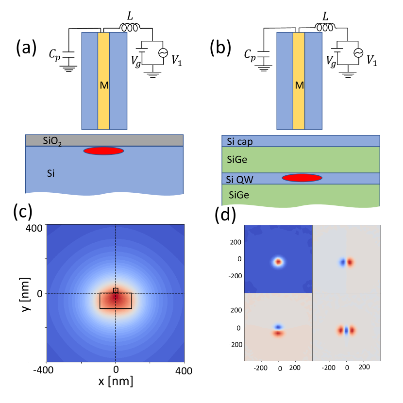
Figure 1 shows schematic pictures of a possible setup. The gate chip containing required trapping and measurement circuitry is placed perpendicular above a semiconductor structure, such as MOS [Fig. 1 (a)] or Si/SiGe QW structure [Fig. 1 (b)]. Applying positive voltage to the gate wire induces a confining electrostatic potential in the 2D quantum well in the structure [Fig. 1 (c)] and orbital wave functions show typical 2D QD orbital characters [Fig. 1 (d)]. Electrons can be trapped into the induced QD as was depicted by red regions in Fig. 1 (a) for MOS and (b) for QW. The energy levels of the induced QDs have nonzero second derivative w.r.t. the applied voltage (i.e. a quantum capacitance), allowing for a dispersive readout by coupling to a detector circuit which can be integrated in the gate chip Colless et al. (2013); Gonzalez-Zalba et al. (2015); Rossi et al. (2017); Urdampilleta et al. (2018).
We performed electrostatic simulation of the deviceCOM using dimensions for MOS and QW devices that are typically used in experiments. For a MOS structureYang et al. (2013); Veldhorst et al. (2014); Maurand et al. (2016); Fogarty et al. (2018), a silicon oxide layer of 10nm overlays the silicon substrate of . For a QW structureKawakami et al. (2014); Zajac et al. (2015), a strained silicon quantum well of 10nm is sandwiched between a SiGe substrate and a SiGe spacer which is capped by 10nm of silicon. We choose a reasonable and manufacturable gate chip design to demonstrate the main concepts in this work. The gate wire size is chosen to be and long, and away from the top of the heterostructure. We considered different sizes of gate wafers as well as a bare metallic wire tip with no gate wafer for the simulations and obtained qualitatively similar results. To be specific, we present below results for the gate wire on a silicon wafer of depth and width.
To conduct measurements of useful device properties, especially for properties relevant for spin qubits, we need to populate the induced quantum dot with a controlled number of electrons. This can be achieved in a number of different ways: e.g., (i) an electron-hole pair can be generated near the induced QD by light, and the electron is trapped to the QD while the hole is pushed away from the QD by the electrostatic force, or (ii) one can dope the semiconductor by implanting donors in a specific region (or use large “electron bath” gate Colless et al. (2013); Rossi et al. (2017)) and use the dot accumulation wire to load electrons from the doped region into the QD (one could then possibly move the electron to another area on the chip as in the STM induced QD device Salfi et al. (2018)). Once isolated, the dot gate voltage can be tuned to enhance the quantum capacitance while maintaining single occupation.
We can detect the charge in the QD via dispersive readoutColless et al. (2013); Gonzalez-Zalba et al. (2015); Rossi et al. (2017); Urdampilleta et al. (2018) by incorporating a tank-circuit (often superconducting) resonator (typically with frequency of a few hundred MHz to a few GHz) into the gate wire and accumulated QD [e.g., Fig. 1(a)], and then sending and reflecting resonant microwaves to it. There would be no phase shift of the reflected signal from an empty dot, but if there is a trapped electron, the reflected signal will be phase shifted if the quantum capacitance Averin et al. (1985); Duty et al. (2005); Sillanpää et al. (2005); Petersson et al. (2010); Cottet et al. (2011); Mizuta et al. (2017); Ruskov and Tahan (2017) of the electron energy level is large enough. We send an rf-signal (along with the DC voltage ): . In addition to the conventional capacitance of the gate-to-heterostructure QD, , and a distributed parasitic capacitance of the gate to the ground plane, as was depicted in Fig.1 (a) and (b), there will be a quantum capacitance of the induced QD, including the lever arm of the tip-to-dot capacitive coupling (here and are the tip-to-dot and dot-to-ground capacitances, respectively; for further estimations we assume ). The quantum capacitance arises from the non-linear voltage response of the QD’s energy levels Ruskov and Tahan (2017), , assuming slow in time voltage perturbation . It leads to a frequency shift of the tank-circuit Ruskov and Tahan (2017), and the corresponding phase shift of the reflected signal due to would be Colless et al. (2013); Gonzalez-Zalba et al. (2015)
| (1) |
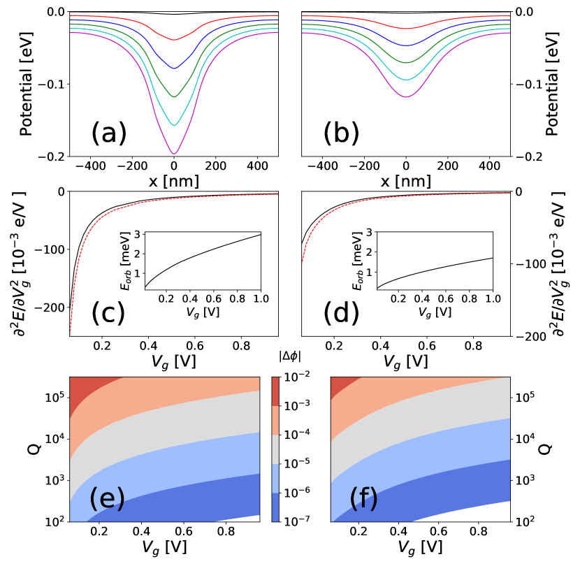
where the Q-factor is defined via the tank-circuit relaxation . [For a single QD level the non-linear voltage response arises from the spatial change of the orbitals, which is often neglected in Hubbard-like Hamiltonians. We recently showed the differences between a Hubbard-like Hamiltonian and the actual induced QD system and its consequences on QD devices.Shim and Tahan (2018)] Figure 2 (a) and (b) show the QD confining potentials at various values for MOS and QW devices, respectively. The second derivative of the orbital energy levels w.r.t the applied is shown in Fig. 2 (c) for MOS and (d) for QW. The absolute value of the quantum capacitance is larger for smaller gate voltage and can be as large as for MOS and for QW at , for the geometry studied in this work.
For typical low tank-circuitsColless et al. (2013); Rossi et al. (2017) having of a few hundred fF (and a frequency in the few hundred MHz range) a capacitance change at level of a few aF is measurableRossi et al. (2017), leading to a phase shift . Figure 2 (e) and (f) show the calculated phase shift for , vs. and from Eq. (1) (assuming ). The sensitivity to measure a small quantum capacitance will increase for moderately large tank-circuit Q-factors, (e.g., the recently proposed high-kinetic inductance nano-wire resonatorsSamkharadze et al. (2018) with frequency of a few GHz and can be used in our proposed vertical gate circuit). As an example, for as per the simulation, and a reachable resonator parametersSamkharadze et al. (2018): , , one can obtain , which is readily measurableGonzalez-Zalba et al. (2015); Rossi et al. (2017). The lowest detectable may be limited by unwanted variation in gate-to-QD capacitance as a function of gate voltage (e.g., due to interface traps below the QD gate Rossi et al. (2017)).
If the device is in a configuration where the induced QD is close to an electron reservoir or another quantum dot, then the charge stability diagram can be mapped out directly using the tunneling capacitance,Petersson et al. (2010) where the response signal peaks at a charge transition (similar to Ref. [Colless et al., 2013]).
As an example of critical material parameters that the separate gate chip could measure, we now discuss how to measure the valley splitting in a silicon wafer. We first examine the case of a single QD with one electron. Following the ideas of Ref. [Yang et al., 2013], a relatively small accumulation mode QD as in Ref. [Rossi et al., 2017] can ensure that the orbital splitting is much larger than the valley splitting, , which allows us to consider only the lowest orbital states in the following analysis. Experimentally, and in small QDs in a MOS deviceYang et al. (2013) and also and in another MOS deviceHao et al. (2014). For quantum dots, could be of the order of , or it could be much smaller. In the simulation of induced dots the above is satisfied as is of the order of meV [see insets of Fig. 2 (c) and (d)].
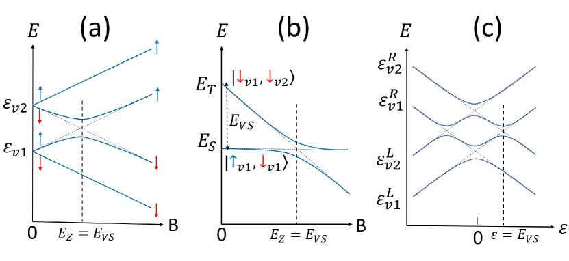
The valley splitting, , depends linearly on the applied top gate voltageYang et al. (2013). By applying an in-plane magnetic field, the lowest two valley states are Zeeman split (with energy splitting ) into 4 levels, as is shown in Fig. 3(a). The levels 2 and 3 (with different valley content) anti-cross when , which leads to levels’ energy curvature w.r.t. the gate voltage . Indeed, the splitting at anti-crossing, can be phenomenologically parameterized with an (intervalley) dipole matrix element Yang et al. (2013); Gamble et al. (2013), implying a charge re-distribution as a result of interface-induced intervalley tunneling and spin-orbit couplingsRuskov et al. (2018). We have estimated Yang et al. (2013) , using a Rashba/Dresselhaus spin-orbit interactions, , induced at the heterostructure interfaceRuskov et al. (2018). The levels 2 and 3 then read: . This was used to describe the relaxation “hot spot” observed in the experiment, which is mainly due to acoustic phonon emissionYang et al. (2013).
Given this explicit level structure we calculate the curvature of the levels with respect to the gate voltage , obtaining the levels’ quantum capacitances, (this quantifies the non-linear response of the QD systemRuskov and Tahan (2017)). In the magnetic field at anti-crossing [Fig. 3 (a)], these quantum capacitances may be strongly enhanced w.r.t. that of the simple orbitals discussed above. The ground state has zero curvature (=0) from this effect, while for levels 2 and 3 one gets , and
| (2) |
with the capacitances sharply peaked near the anti-crossing (using a simple model with linear dependence on for the valley splittingRuskov et al. (2018)). With the experimentally estimated and valley splitting slopeYang et al. (2013) , we obtain (for ) , which should be measurable in experimentsGonzalez-Zalba et al. (2015); Rossi et al. (2017). Another capacitance contribution may appear due to fast relaxation processesMizuta et al. (2017). While the relaxation rate strongly increases at the spin-valley anti-crossing for a single electron QDYang et al. (2013) (reaching ), it is much slower than the chosen tank-circuit frequencies, , thus suppressing this capacitance contributionMizuta et al. (2017). A way to enhance is to use the in-plane magnetic field with an angle such that becomes much smallerRuskov et al. (2018), however making smaller will narrow the region where is significantly non-zero.
By scanning (sweeping) the magnetic field we will register a sharp peak of phase change of the reflected signal when the Zeeman splitting is . For this to work, we need to populate the excited states by choosing a temperature comparable to the valley splitting, e.g. for the temperature should be . Since , the populations of the levels 2 and 3 in Fig. 3(a) will be comparable, thus leading to an effective quantum capacitance suppression by .
A way to mitigate these effects would be to use a single QD with two electrons. As shown in Fig. 3(b), the lowest two levels now anti-cross at with an anti-crossing splitting (scf. Ref. [Yang et al., 2013]), and the quantum capacitance is the same as in the 1-electron case, while the relaxation is strongly suppressed at anti-crossing. Also, the suppression effect due to temperature will not be as strong as in the 1-electron case, since and so . Since, however, we are in a regime (opposite to that where a quantum capacitance approximation is valid) the effective quantum capacitance is suppressed by a form factor: . E.g., for the suppression factor is . Thus, this method would be sufficient to measure not too small valley splitting.
An alternative method to measure the valley splitting with a slightly more complicated gate circuit is to induce a double QD using two or three gate wires on the gate chip. Let us consider a DQD with a single electron, assuming each QD has the same valley splitting. The detuning between the QDs can be changed by tuning the voltages on the two QD-defining gates. At zero detuning (), one is at the degeneracy point of the lower eigenvalley -electrons. [ is the lower valley and is the upper valley states. See Fig. 3(c)]. The left-right tunneling between the dots defines the splitting at anti-crossing, . One then can measure the change of the reflected signal at the degeneracy point (where the energy curvature is maximal) using a tank-circuit frequency . By sweeping the detuning to the -electron from the left can tunnel to the -level from the right. This tunneling possibility forms another anti-crossing and corresponding splitting (assume the same ). (This kind of tunneling is briefly discussed in Ref. [Hao et al., 2014] and then at length in Ref. [Burkard and Petta, 2016].)
To measure the valley splitting, one starts at , and populates the lowest two levels by temperature. One then moves (faster than the relaxation time ) to a detuning , while sending a microwave with , to encounter a sharp change in the reflected phase (provided that ). This can be fulfilled for and . Once is reached, the reflected signal changes accordingly, due to maximal quantum capacitance similar to the experiment of Pettersson et al.Petersson et al. (2010). The quantum capacitance at this anti-crossing is estimated of the order of , which is several orders of magnitude larger than at the spin-valley anti-crossing discussed above. In order to be able to distinguish the anti-crossings at and at , one needs which sets the lowest measurable valley splitting, . The main difference of this proposal from that of Ref. [Burkard and Petta, 2016] is that the probing signal is far off resonance with the level splitting, at a constant tank-circuit frequency , and the signature of valley splitting is easier to measure. These last two cases - doubly occupied single QD and a singly occupied DQD - may be the easiest to experimentally implement as a first verification of this proposed methodology.
Finally, we note that an additional (tunable) microwave field can be introduced to the above proposed experiments to drive transitions between quantum dot states, which may allow for further or improved characterization (and also introduces another absolute energy scale to compare to, in addition to the magnetic field).
The proposal presented in this paper requires sensitive measurement of small (quantum) capacitance changes, , in sub-aF to aF range. The signal due to may be obscured, however, in the presence of noise of the large fluctuating capacitances, , (see Fig. 1). For example, fluctuations via the voltage dependence of are attributed to the charging of interface traps below the QD gate Rossi et al. (2017); the corresponding noise variation would be where is the voltage spectral density and is an averaging time. It was experimentally shown that below a sample-specific voltage threshold, , the capacitance derivative is small and a capacitance change of was resolved Rossi et al. (2017). Another type of noise may enter through mechanical fluctuations of the tip. See e.g. experiments with Scanning Microwave Microscopy (SMM) Gramse et al. (2017); de Graaf et al. (2013). In an experiment of near-field SMM de Graaf et al. (2013) the (slow) resonator frequency fluctuations are tracked and stabilized via a feedback loop allowing longer averaging time to reduce the noise; a sensitivity of was limited by mechanical noisede Graaf et al. (2013). Since in our proposed experiment the tip is not moving, the mechanical noise may be reduced, eventually allowing for valley splitting measurement via a tip-induced QD in the Si heterostructure.
Inducing quantum dots instead of fabricating them offers the potential for non-destructive characterization either locally or across a wafer, speeding optimization of materials and quantum devices such as qubits. Our concept is applicable to other materials and systems as the inducing and measurement chip can be fabricated on a substrate different from the materials system under consideration. We show that inducing QDs and measuring valley splitting in silicon devices is plausible with current experimental technology. Induced QD devices and the actual quantum devices built on the wafer will be different, but they share many critical aspects of the underlying material. Characterization of the induced QD devices will provide useful information of the yet-to-be-built devices. Based on this concept, other materials and systems (germanium, holes instead of electrons, topological systems, etc.) and qubit approaches (encoded qubits, different readout techniques, even linear arrays of qubits making small quantum computers) can be explored without actually fabricating the quantum dots themselves.
We thank Bob Butera and Michael Dreyer for helpful discussion. H.M.H. acknowledges support from the NPSC fellowship.
References
- Zwanenburg et al. (2013) F. A. Zwanenburg, A. S. Dzurak, A. Morello, M. Y. Simmons, L. C. L. Hollenberg, G. Klimeck, S. Rogge, S. N. Coppersmith, and M. A. Eriksson, Rev. Mod. Phys. 85, 961 (2013).
- Maiwald et al. (2009) R. Maiwald, D. Leibfried, J. Britton, J. C. Bergquist, G. Leuchs, and D. J. Wineland, Nat. Phys. 5, 551 (2009).
- Arrington et al. (2013) C. L. Arrington, K. S. McKay, E. D. Baca, J. J. Coleman, Y. Colombe, P. Finnegan, D. A. Hite, A. E. Hollowell, R. Jördens, J. D. Jost, D. Leibfried, A. M. Rowen, U. Warring, M. Weides, A. C. Wilson, D. J. Wineland, and D. P. Pappas, Rev. Sci. Instrum. 84, 085001 (2013).
- Casola et al. (2018) F. Casola, T. van der Sar, and A. Yacoby, Nat. Rev. Mater. 3, 17088 (2018).
- Wittneven et al. (1998) C. Wittneven, R. Dombrowski, M. Morgenstern, and R. Wiesendanger, Phys. Rev. Lett. 81, 5616 (1998).
- Dombrowski et al. (1999) R. Dombrowski, C. Steinebach, C. Wittneven, M. Morgenstern, and R. Wiesendanger, Phys. Rev. B 59, 8043 (1999).
- Salfi et al. (2018) J. Salfi, B. Voisin, A. Tankasala, J. Bocquel, M. Usman, M. Y. Simmons, L. C. L. Hollenberg, R. Rahman, and S. Rogge, Phys. Rev. X 8, 031049 (2018).
- Bussmann et al. (2015) E. Bussmann, M. Rudolph, G. S. Subramania, S. Misra, S. M. Carr, E. Langlois, J. Dominguez, T. Pluym, M. P. Lilly, and M. S. Carroll, Nanotechnology 26, 085701 (2015).
- Gramse et al. (2017) G. Gramse, A. Kölker, T. Lim, T. J. Z. Stock, H. Solanki, S. R. Schofield, E. Brinciotti, G. Aeppli, F. Kienberger, and N. J. Curson, Sci. Adv. 3, e1602586 (2017).
- Colless et al. (2013) J. I. Colless, A. C. Mahoney, J. M. Hornibrook, A. C. Doherty, H. Lu, A. C. Gossard, and D. J. Reilly, Phys. Rev. Lett. 110, 046805 (2013).
- Gonzalez-Zalba et al. (2015) M. Gonzalez-Zalba, S. Barraud, A. Ferguson, and A. Betz, Nat. Commun. 6, 6084 (2015).
- Rossi et al. (2017) A. Rossi, R. Zhao, A. S. Dzurak, and M. F. Gonzalez-Zalba, Appl. Phys. Lett. 110, 212101 (2017).
- Urdampilleta et al. (2018) M. Urdampilleta, D. J. Niegemann, E. Chanrion, B. Jadot, C. Spence, P.-A. Mortemousque, C. Bäuerle, L. Hutin, B. Bertrand, S. Barraud, R. Maurand, M. Sanquer, X. Jehl, S. D. Franceschi, M. Vinet, and T. Meunier, “Gate-based high fidelity spin readout in a CMOS device,” (2018), arXiv:1809.04584 [cond-mat] .
- (14) COMSOL Multiphysics® v.5.3. www.comsol.com. COMSOL AB, Stockholm, Sweden.
- Yang et al. (2013) C. H. Yang, A. Rossi, R. Ruskov, N. S. Lai, F. A. Mohiyaddin, S. Lee, C. Tahan, G. Klimeck, A. Morello, and A. S. Dzurak, Nat. Commun. 4, 2069 (2013).
- Veldhorst et al. (2014) M. Veldhorst, J. C. C. Hwang, C. H. Yang, A. W. Leenstra, B. de Ronde, J. P. Dehollain, J. T. Muhonen, F. E. Hudson, K. M. Itoh, A. Morello, and A. S. Dzurak, Nat. Nanotechnol. 9, 981 (2014).
- Maurand et al. (2016) R. Maurand, X. Jehl, D. Kotekar-Patil, A. Corna, H. Bohuslavskyi, R. Laviéville, L. Hutin, S. Barraud, M. Vinet, M. Sanquer, and S. D. Franceschi, Nat. Commun. 7, 13575 (2016).
- Fogarty et al. (2018) M. A. Fogarty, K. W. Chan, B. Hensen, W. Huang, T. Tanttu, C. H. Yang, A. Laucht, M. Veldhorst, F. E. Hudson, K. M. Itoh, D. Culcer, T. D. Ladd, A. Morello, and A. S. Dzurak, Nat. Commun. 9, 4370 (2018).
- Kawakami et al. (2014) E. Kawakami, P. Scarlino, D. R. Ward, F. R. Braakman, D. E. Savage, M. G. Lagally, M. Friesen, S. N. Coppersmith, M. A. Eriksson, and L. M. K. Vandersypen, Nat. Nanotechnol. 9, 666 (2014).
- Zajac et al. (2015) D. M. Zajac, T. M. Hazard, X. Mi, K. Wang, and J. R. Petta, Appl. Phys. Lett. 106, 223507 (2015).
- Averin et al. (1985) D. V. Averin, A. B. Zorin, and K. K. Likharev, Sov. Phys. JETP 61, 407 (1985).
- Duty et al. (2005) T. Duty, G. Johansson, K. Bladh, D. Gunnarsson, C. Wilson, and P. Delsing, Phys. Rev. Lett. 95, 206807 (2005).
- Sillanpää et al. (2005) M. A. Sillanpää, T. Lehtinen, A. Paila, Y. Makhlin, L. Roschier, and P. J. Hakonen, Phys. Rev. Lett. 95, 206806 (2005).
- Petersson et al. (2010) K. D. Petersson, C. G. Smith, D. Anderson, P. Atkinson, G. A. C. Jones, and D. A. Ritchie, Nano Lett. 10, 2789 (2010).
- Cottet et al. (2011) A. Cottet, C. Mora, and T. Kontos, Phys. Rev. B 83, 121311(R) (2011).
- Mizuta et al. (2017) R. Mizuta, R. M. Otxoa, A. C. Betz, and M. F. Gonzalez-Zalba, Phys. Rev. B 95, 045414 (2017).
- Ruskov and Tahan (2017) R. Ruskov and C. Tahan, “Quantum-limited measurement of spin qubits via curvature coupling to a cavity,” (2017), arXiv:1704.05876v1 [cond-mat] .
- Shim and Tahan (2018) Y.-P. Shim and C. Tahan, Phys. Rev. B 97, 155402 (2018).
- Samkharadze et al. (2018) N. Samkharadze, G. Zheng, N. Kalhor, D. Brousse, A. Sammak, U. C. Mendes, A. Blais, G. Scappucci, and L. M. K. Vandersypen, Science 359, 1123 (2018).
- Hao et al. (2014) X. Hao, R. Ruskov, M. Xiao, C. Tahan, and H. Jiang, Nat. Commun. 5, 3860 (2014).
- Gamble et al. (2013) J. K. Gamble, M. A. Eriksson, S. N. Coppersmith, and M. Friesen, Phys. Rev. B 88, 035310 (2013).
- Ruskov et al. (2018) R. Ruskov, M. Veldhorst, A. S. Dzurak, and C. Tahan, Phys. Rev. B 98, 245424 (2018).
- Burkard and Petta (2016) G. Burkard and J. R. Petta, Phys. Rev. B 94, 195305 (2016).
- de Graaf et al. (2013) S. E. de Graaf, A. V. Danilov, A. Adamyan, and S. E. Kubatkin, Rev. Sci. Instrum. 84, 023706 (2013).