Polarizability and impurity screening for phosphorene
Abstract
Using a tight-binding Hamiltonian for phosphorene, we have calculated the real part of the polarizability and the corresponding dielectric function, Re[], at zero temperature (T = 0) with free carrier density . We present results showing Re[] in different directions of the transferred momentum . When is larger than a particular value which is twice the Fermi momentum , Re[] becomes strongly dependent on the direction of . We also discuss the case at room temperature (T = 300K). These results which are similar to those previously reported by other authors are then employed to determine the static shielding of an impurity in the vicinity of phosphorene.
pacs:
73.21.-b, 71.70.Ej, 73.20.Mf, 71.45.Gm, 71.10.Ca, 81.05.ueI Introduction
Emerging phenomena in physics and quantum information technology have relied extensively on the collective properties of low-dimensional materials such as two-dimensional (2D) and few-layer structures with nanoscale thickness. There, the Coulomb and/or atomic interactions play a crucial role in these complexes which include doped as well as undoped graphene GR1 ; GR2 ; GR3 , silicene Si4 ; Si5 , phosphorene BP9 ; BP10 , germanene Ge6 ; Ge7 , antimonene Sb11 ; Sb12 , tinene Ti8 , bismuthene Bi13 ; Bi14 ; Bi15 ; Bi16 ; Bi17 ; Bi18 and most recently the 2D pseudospin-1 lattice Ejnicol . Of these which have been successfully synthesized by various experimental techniques and which have been extensively investigated by various experimental techniques, few-layer black phosphorus (phosphorene) or BP has been produced by using mechanical cleavage PLi2014 ; PLiu2014 , liquid exfoliation PBrent2014 ; BP10 ; Pkang2015 , and mineralizer-assisted short-way transport reaction PLange2007 ; PNilges2008 ; PKopf2014 .
Unlike graphene, phosphorus inherently has an appreciable band gap. The observed photoluminescence peak of single-layer phosphorus in the visible optical range shows that its band gap is larger than that for bulk. Furthermore, BP has a middle energy gap ( eV) at the point, thereby being quite different from the narrow or zero gaps of group-IV systems. Specifically, experimental measurements have shown that the BP-based field effect transistor has an on/off ratio of 105 and a carrier mobility at room temperature as large as 103 cmVs. We note that BP is expected to play an important role in the next-generation of electronic devices PLi2014 ; PLiu2014 . Phosphorene exhibits a puckered structure related to the hybridization of () orbitals. The deformed hexagonal lattice of monolayer BP has four atoms PRudenko , while the group-IV honeycomb lattice includes two atoms. The low-lying energy dispersions, which are dominated by orbitals, can be described by a four-band model with complicated multi-hopping integrals PRudenko . The low-lying energy bands are highly anisotropic, e.g., the linear and parabolic dispersions near the Fermi energy , respectively, along the and directions. The anisotropic behaviors are further reflected in other physical properties, as verified by recent measurements on optical and excitonic spectra Oleg as well as transport properties PLi2014 ; PLow .
In this work, we have examined the anisotropic behavior of the static polarizability and shielded potential of an impurity for BP. The calculations for the polarizability were executed at T=0K and room temperature (T=300K). We treat the buckled BP structure as a 2D sheet in our formalism. Consequently, we present an algebraic expression for the surface response function of a pair of 2D layers with arbitrary separation and which are embedded in dielectric media. We then adapt this result to the case when the layer separation is very small to model a free-standing buckled BP structure.
The outline of the rest of our presentation is as follows. In Sec. II, we present the surface response function for a pair of 2D layers embedded in background dielectric media. We then simplify this result for a pair of planar sheets which are infinitesimally close to each other and use this for buckled BP. The tight-binding model Hamiltonian for BP is presented in Sec. III. This is employed in our calculations of the energy bands and eigenfunctions. Section IV. is devoted to the calculation of the polarizability and dielectric function of BP showing its temperature dependence and their anisotropic properties as a consequence of its band structure. Impurity shielding by BP is discussed in Sec. V and we summarize our important results in Sec. VI.
II Surface response function for a pair of 2D layers
The external potential will give rise to an induced potential which, outside the structure, can be written as
| (1) |
This equation defines the surface response function . It has been implicitly assumed that the external potential is so weak that the medium responds linearly to it.
The quantity Im[g(] can be identified with the power absorption in the structure due to electron excitation induced by the external potential. The total potential in the vicinity of the surface (), is given by
| (2) |
which takes account of nonlocal screening of the external potential.
II.1 Model for phosphorene layer
In this section, we present the surface repsonse function we calculated for a structure which consists of a pair of 2D layers in contact with a dielectric medium, as shown in Figure 1 . One of the 2D layers is at the top and the other is encapsulated by materials with dielectric constants , with thickness , and , of semi-infinite thickness. Calculation shows that the surface response function is given by Book ; PRB2018
| (3) |
where
| (4) | |||||
and
| (5) | |||||
In this notation, is the in-plane wave vector, is the frequency and and are the 2D layer susceptibilities.
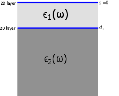
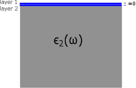
When we take the limit , i.e., the separation between the two layer is small, the drops out and we have the following result for the surface response function corresponding to the structure in Figure 2
| (6) |
Here, the dispersion equation which is given by the zeros of the denominator of the second term is expressed in terms of the ’average’ susceptibility for the two layers. Clearly, this dispersion equation is that for a 2D layer of the Stern form where we make the identification in terms of the polarizability. This result in Eq. (6) clearly illustrates that for the buckled BP structure shown in Figure 3, the dielectric function can be treated as that for a single layer whose susceptibility arises from a combination of two rows of atoms making up the layer. Our calculation can easily be generalized to the case when the monolayer is embedded above and below by the same thick dielectric material (dielectric constant ) which corresponds to the free-standing situation which we consider below. For this, we have , expressed in terms of the 2D layer polarizability .
III Model Hamiltonian
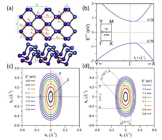
Phosphorene is treated as a single layer of phosphorus atoms arranged in a puckered orthorhombic lattice, as shown in Fig. 3(a). It contains two atomic layers of A and B atoms and two kinds of bonds for in-plane and inter-plane P-P connections with different bond lengths. The low-lying electronic structure can be described by a tight-binding Hamiltonian, which is a 4 4 matrix within the basis (, , , ), of the form
Here, we consider up to five nearest atomic interactions through five independent terms of with . These terms are given by the following expressions.
| (12) |
In this notation, () are the hopping integrals, corresponding to the atomic interactions. They have been optimized as (, , , , ) in order to reproduce the energy bands obtained by the density functional theory (DFT) calculations dft1 ; dft2 ; tbm1 . Also, are the vectors connecting the lattice sites which can be written as
| (18) |
where , , , and are the distances between the BP atoms tbm2 ; tbm3 , as illustrated in Figure 3(a).
The valence and conduction energy bands present strong anisotropic behaviors, as illustrated by the energy bands in Fig. 3(b) and the constant-energy loops in Figs. 3(c) and 3(d). As a result, the polarizability and dielectric function are shown to be strongly dependent on the direction of the transferred momentum .
IV Dielectric Function
When monolayer BP is perturbed by an external time-dependent Coulomb potential, all the valence and conduction electrons will screen this field and therefore create the charge redistribution. The effective potential between two charges is the sum of the external potential and the induced potential due to screening charges. The dynamical dielectric function, within the random-phase approximation (RPA), is given by diele
| (19) | |||
Here, the -electronic excitations are described in terms of the transferred momentum and the excitation frequency . the background dielectric constant, 2 the 2D Fourier transform of the bare Coulomb potential energy (), and the energy width due to various de-excitation mechanisms. the Fermi-Dirac distribution in which is the Boltzmann constant and the chemical potential corresponding to the highest occupied state energy (middle energy of band gap) in the (semiconducting) metallic systems at T=0.
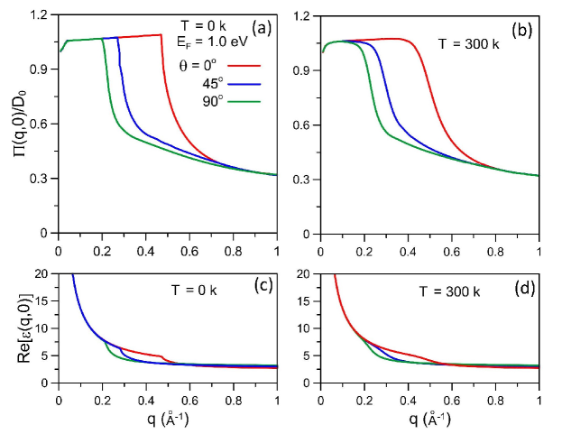
Figures 4(a) and 4(b) show the directional/-dependence of the static polarization function , in which defines the angle between the direction of and the unit vector . For arbitrary , the polarization function at lower ( 0.2 ()) and higher ( 0.7 ()) transferred momentum remains unchanged. In general, falls off rapidly beyond a critical value of (2) which depends on . For increasing from 0 to , the specific values are getting larger, as shown in Fig. 4(a). This means that the polarizability is stronger for 0.2 0.7 (). The main features of the polarizability for BP are quite similar to those for the 2D electron gas, but different with those for graphene. Temperature has an effect on the polarization function which is demonstrated in Fig. 4(b). At room temperature, exhibits a shoulder-like structure near the critical values of instead of step-like structure at T = 0.
Plots of the static dielectric function of BP for various values of are presented in Figs. 4(c) and 4(d) at zero and room temperatures, respectively. In the range of 0.2 0.5 (), there is a clear dependence of the dielectric function on the direction of the transferred momentum . The Re is higher with the growth of . The introduction of finite temperature smoothens the -dependent Re , as shown in Fig. 4(d) for T = 300K.
V Impurity shielding
Starting with Eq. (2), we obtain the static screening of the potential on the surface at due to an impurity with charge located at distance above the surface of BP as
| (20) | |||||
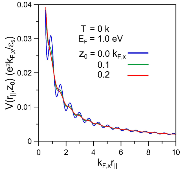
By employing the generalized form of Eq. (6) for free-standing BP in Eq. (20), we have computed the screened impurity potential. The screened potentials for various ’s are shown in Fig. 5 at zero temperature and Fermi energy = 1.0 eV. There exist Friedel oscillations for sufficiently small . Such oscillations might be smeared out for larger , e.g., the green and red curves. It is noticed that for = 1.0 eV, the room temperature of 300K which is much smaller than the Fermi temperature (10000K) does not have significant effect on the screened potential. Apparently, at T = 0 and T = 300K (not shown) are almost equivalent.
VI Concluding Remarks and Summary
The energy band structure of BP, calculated using the tight-binding method, is anisotropic and so are its polarizability, dielectric function and screened potential. To illustrate these facts, we have presented numerical results for the polarizability in the and directions for a range of doping concentrations. The Re[] of the static dielectric function for BP also reveals some interesting characteristics. At zero temperature (T = 0) and with free carrier density corresponding to chosen Fermi energy , we have presented numerical results for Re[] in different directions of the transferred momentum . When is larger than a critical value which is twice the Fermi momentum , our calculations show that Re[] becomes substantially dependent on the direction of . We also discuss the case at room temperature (T = 300K). These results are in agreement with those reported by other authors. We employ our data to determine the static shielding of an impurity in the vicinity of phosphorene.
Conflict of interest
All the authors declare that they have no conflict of interest.
Acknowledgements.
G.G. would like to acknowledge the support from the Air Force Research Laboratory (AFRL) through Grant #12530960 . ReferencesReferences
- (1) Novoselov KS, Geim AK, Morozov SV, Jiang D, Zhang Y, Dubonos SV, et al. Electric field effect in atomically thin carbon films. Science. 2004;306:666-9. DOI: 10.1126/science.1102896
- (2) D bbelin M, Ciesielski A, Haar S, Osella S, Bruna M, Minoia A, et al. Light-enhanced liquid-phase exfoliation and current photoswitching in graphene-azobenzene composites. Nature Communications. 2016;7:11090. DOI: 10.1038/ncomms11090
- (3) Kim KS, Zhao Y, Jang H, Lee SY, Kim JM, Kim KS, et al. Large-scale pattern growth of graphene films for stretchable transparent electrodes. Nature. 2009;457:706-10. DOI: 10.1038/nature07719
- (4) Tao L, Cinquanta E, Chiappe D, Grazianetti C, Fanciulli M, Dubey M, et al. Silicene field-effect transistors operating at room temperature. Nature Nanotechnology. 2015;10:227-31. DOI: 10.1038/nnano.2014.325
- (5) Vogt P, De Padova P, Quaresima C, Avila J, Frantzeskakis E, Asensio MC, et al. Silicene: Compelling Experimental Evidence for Graphenelike Two-Dimensional Silicon. Phys Rev Lett. 2012;108:155501. DOI: 10.1103/PhysRevLett.108.155501
- (6) Li L, Yu Y, Ye GJ, Ge Q, Ou X, Wu H, et al. Black phosphorus field-effect transistors. Nature Nanotechnology. 2014;9:372-7. DOI: 10.1038/nnano.2014.35
- (7) Yasaei P, Kumar B, Foroozan T, Wang C, Asadi M, Tuschel D, et al. High-Quality Black Phosphorus Atomic Layers by Liquid-Phase Exfoliation. Advanced Materials. 2015;27:1887-92. DOI: 10.1002/adma.201405150
- (8) Li L, Lu S, Pan J, Qin Z, Wang Y, Wang Y, et al. Buckled Germanene Formation on Pt(111). Advanced Materials. 2014;26:4820-4. DOI: 10.1002/adma.201400909
- (9) Derivaz M, Dentel D, Stephan R, Hanf M-C, Mehdaoui A, Sonnet P, et al. Continuous Germanene Layer on Al(111). Nano Lett. 2015;15:2510-6. DOI: 10.1021/acs.nanolett.5b00085
- (10) Ji J, Song X, Liu J, Yan Z, Huo C, Zhang S, et al. Two-dimensional antimonene single crystals grown by van der Waals epitaxy. Nature Communications. 2016;7:13352. DOI: 10.1038/ncomms13352
- (11) Ares P, Aguilar Galindo F, Rodr guez San Miguel D, Aldave DA, D az Tendero S, Alcam M, et al. Antimonene: Mechanical Isolation of Highly Stable Antimonene under Ambient Conditions. Advanced Materials. 2016;28:6515-6515. DOI: 10.1002/adma.201670209
- (12) Zhu F, Chen W, Xu Y, Gao C, Guan D, Liu C, et al. Epitaxial growth of two-dimensional stanene. Nat Mater. 2015;14:1020-5. DOI: 10.1038/nmat4384
- (13) Hirahara T, Nagao T, Matsuda I, Bihlmayer G, Chulkov EV, Koroteev YM, et al. Role of Spin-Orbit Coupling and Hybridization Effects in the Electronic Structure of Ultrathin Bi Films. Phys Rev Lett. 2006;97:146803. DOI: 10.1103/PhysRevLett.97.146803
- (14) Hirahara T, Shirai T, Hajiri T, Matsunami M, Tanaka K, Kimura S, et al. Role of Quantum and Surface-State Effects in the Bulk Fermi-Level Position of Ultrathin Bi Films. Phys Rev Lett. 2015;115:106803. DOI: 10.1103/PhysRevLett.115.106803
- (15) Hirahara T, Fukui N, Shirasawa T, Yamada M, Aitani M, Miyazaki H, et al. Atomic and Electronic Structure of Ultrathin Bi(111) Films Grown on Substrates: Evidence for a Strain-Induced Topological Phase Transition. Phys Rev Lett. 2012;109:227401. DOI: 10.1103/PhysRevLett.109.227401
- (16) Yang F, Miao L, Wang ZF, Yao M-Y, Zhu F, Song YR, et al. Spatial and Energy Distribution of Topological Edge States in Single Bi(111) Bilayer. Phys Rev Lett. 2012;109:016801. DOI: 10.1103/PhysRevLett.109.016801
- (17) Wang ZF, Yao M-Y, Ming W, Miao L, Zhu F, Liu C, et al. Creation of helical Dirac fermions by interfacing two gapped systems of ordinary fermions. Nature Communications. 2013;4:1384. DOI: 10.1038/ncomms2387
- (18) Sabater C, Gos lbez-Mart nez D, Fern ndez-Rossier J, Rodrigo JG, Untiedt C, Palacios JJ. Topologically Protected Quantum Transport in Locally Exfoliated Bismuth at Room Temperature. Phys Rev Lett. 2013;110:176802. DOI: 10.1103/PhysRevLett.110.176802
- (19) Malcolm JD, Nicol EJ. Frequency-dependent polarizability, plasmons, and screening in the two-dimensional pseudospin-1 dice lattice. Phys Rev B. 2016;93:165433. DOI: 10.1103/PhysRevB.93.165433
- (20) Li L, Yu Y, Ye GJ, Ge Q, Ou X, Wu H, et al. Black phosphorus field-effect transistors. Nature Nanotechnology. 2014;9:372-7. DOI: 10.1038/nnano.2014.35
- (21) Liu H, Neal AT, Zhu Z, Luo Z, Xu X, Tom nek D, et al. Phosphorene: An Unexplored 2D Semiconductor with a High Hole Mobility. ACS Nano. 2014;8:4033-41. DOI: 10.1021/nn501226z
- (22) Brent JR, Savjani N, Lewis EA, Haigh SJ, Lewis DJ, O’Brien P. Production of few-layer phosphorene by liquid exfoliation of black phosphorus. Chem Commun. 2014;50:13338-41. DOI: 10.1039/C4CC05752J
- (23) Kang J, Wood JD, Wells SA, Lee J-H, Liu X, Chen K-S, et al. Solvent Exfoliation of Electronic-Grade, Two-Dimensional Black Phosphorus. ACS Nano. 2015;9:3596-604. DOI: 10.1021/acsnano.5b01143
- (24) Lange S, Schmidt P, Nilges T. Au3SnP7@Black Phosphorus: An Easy Access to Black Phosphorus. Inorg Chem. 2007;46:4028-35. DOI: 10.1021/ic062192q
- (25) Nilges T, Kersting M, Pfeifer T. A fast low-pressure transport route to large black phosphorus single crystals. Journal of Solid State Chemistry. 2008;181:1707-11. DOI: 10.1016/j.jssc.2008.03.008
- (26) K pf M, Eckstein N, Pfister D, Grotz C, Kr ger I, Greiwe M, et al. Access and in situ growth of phosphorene-precursor black phosphorus. Journal of Crystal Growth. 2014;405:6-10. DOI: 10.1016/j.jcrysgro.2014.07.029
- (27) Berman OL, Gumbs G, Kezerashvili RY. Bose-Einstein condensation and superfluidity of dipolar excitons in a phosphorene double layer. Phys Rev B. 2017;96:014505. DOI: 10.1103/PhysRevB.96.014505
- (28) Rudenko AN, Katsnelson MI. Quasiparticle band structure and tight-binding model for single- and bilayer black phosphorus. Phys Rev B. 2014;89:201408. DOI: 10.1103/PhysRevB.89.201408
- (29) Low T, Rodin AS, Carvalho A, Jiang Y, Wang H, Xia F, et al. Tunable optical properties of multilayer black phosphorus thin films. Phys Rev B. 2014;90:075434. DOI: 10.1103/PhysRevB.90.075434
- (30) Gumbs G, Huang D. Properties of Interacting Low-Dimensional Systems. 1st ed. New York: Wiley; 2011. 113 p. DOI: 10.1002/9783527638154.
- (31) Dahal D, Gumbs G, Huang D. Effect of strain on plasmons, screening, and energy loss in graphene/substrate contacts. Phys Rev B. 2018;98:045427. DOI: 10.1103/PhysRevB.98.045427.
- (32) Heyd J, Scuseria GE, Ernzerhof M. Hybrid functionals based on a screened Coulomb potential. The Journal of Chemical Physics. 2003;118:8207-15. DOI: 10.1063/1.1564060
- (33) Heyd J, Scuseria GE, Ernzerhof M. Erratum. Hybrid functionals based on a screened Coulomb potential. The Journal of Chemical Physics. 2006;124:219906. DOI: 10.1063/1.2204597
- (34) P ez CJ, DeLello K, Le D, Pereira ALC, Mucciolo ER. Disorder effect on the anisotropic resistivity of phosphorene determined by a tight-binding model. Phys Rev B. 2016;94:165419. DOI: 10.1103/PhysRevB.94.165419
- (35) Takao Y, Asahina H, Morita A. Electronic Structure of Black Phosphorus in Tight Binding Approach. J Phys Soc Jpn. 1981;50:3362-9. DOI: 10.1143/JPSJ.50.3362
- (36) Osada T. Edge State and Intrinsic Hole Doping in Bilayer Phosphorene. J Phys Soc Jpn. 2014;84:013703. DOI: 10.7566/JPSJ.84.013703
- (37) Shung KW-K. Dielectric function and plasmon structure of stage-1 intercalated graphite. Phys Rev B. 1986;34:979-93. DOI: 10.1103/PhysRevB.34.979