Quantum coherent multi-electron processes in an atomic scale contact
Abstract
The light emission from a scanning tunneling microscope operated on a Ag(111) surface at 6 K is analyzed from low conductances to values approaching the conductance quantum. Optical spectra recorded at a sample voltages reveal emission with photon energies A model of electrons interacting coherently via a localized plasmon-polariton mode reproduces the experimental data, in particular the kinks in the spectra at and as well as the scaling of the intensity at low and intermediate conductances.
pacs:
72.70.+m,68.37.Ef,73.63.Rt,73.20.MfA biased nanoscale junction between metal electrodes is a useful environment to study links between quantum transport and electrodynamics. On one hand, very high current densities may be achieved for electrons at energies beyond the Fermi level. On the other hand, such junctions support localized plasmon modes that drastically enhance electromagnetic fields Lambe and McCarthy (1976); Berndt et al. (1993); Atay et al. (2004); Romero et al. (2006); Savage et al. (2012); Marinica et al. (2015); Vardi et al. (2016). A consequence of this coincidence is that light affects the conductance of the junction Möller et al. (1991); Völcker et al. (1991); Guhr et al. (2007), another one is the emission of photons, which is driven by the shot noise of the current and corresponds to inelastic tunneling processes Berndt et al. (1991); Schneider et al. (2010); Le Moal et al. (2016); Kuhnke et al. (2017). Recently, the latter process has been used to electrically drive optical antennas Bharadwaj et al. (2011); Kern et al. (2015).
In addition to the emission at energies (denoted light), where is the applied bias, higher photon energies ( light) have also been observed from metallic and molecular junctions Pechou et al. (1998); Downes et al. (2002); Hoffmann et al. (2003); Dong et al. (2004); Uemura et al. (2007); Schull et al. (2009); Dong et al. (2010); Fujiki et al. (2011); Schneider et al. (2013). For the observations from single-atom junctions in a scanning tunneling microscope (STM), two models have been proposed. Xu et al. Xu et al. (2014, 2016) considered a single, local plasmon-polariton mode modelled by an LC circuit, and attributed the emission to the non-Gaussian quantum noise of the current. Kaasbjerg and Nitzan calculated the current noise to higher order in the electron–plasmon interaction and found that a plasmon-mediated electron–electron interaction is the source of experimentally observed above-threshold light emission Kaasbjerg and Nitzan (2015). The interpretation in terms of coherent processes has been challenged on the basis of experimental data from Au junctions prepared by electromigration and heating of the electron gas has been suggested to lead to the emission at Buret et al. (2015). Black-body radiation from heated electrons had previously been invoked in Ref. Downes et al. (2002).
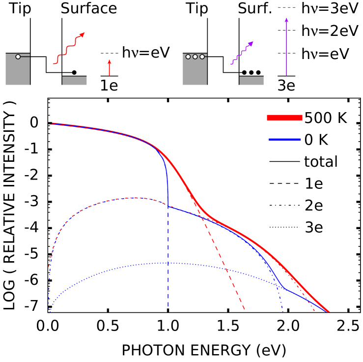
In this Letter we report on the emission of and light from junctions between a STM tip and a Ag(111) single crystal surface. Optical spectra reveal kinks at and and the emission intensity varies in a characteristic manner with the junction conductance. The observations are consistently explained by a model of coherent multi-electron scattering off the local plasmon field via the higher-order processes sketched in the top panel of Fig. 1. It leads to the overall behavior of the emission shown in Fig. 1 (bottom) where processes involving and 3 electrons add up to a total intensity, that —at low temperature— exhibits characteristic kinks at the photon energies , where is the sample voltage. Our work identifies the overbias emission and the corresponding kinks as distinct fingerprints of higher-order electron-plasmon scattering processes, and at the same time indicates insignificant electronic heating in STM contacts.
We used an ultra-high vacuum STM operated at a base temperature of 6 K. Ag(111) samples and electrochemically etched Ag tips were prepared by cycles of Ar ion bombardment and annealing. After inserting the tips into the STM, they were processed by repeated contact formation at sample voltages up to 2 V until the tips were stable Castellanos-Gomez et al. (2012). Experiments were conducted on atomically flat terraces. Light emitted from the tip-sample junction was collected with a lens in-vacuo, then focused onto an optical fiber connected to a grating spectrometer and a thermoelectrically cooled CCD camera Hoffmann et al. (2002). The spectrometer/CCD setup could be exchanged for a photomultiplier tube (PMT) for more sensitive measurement.
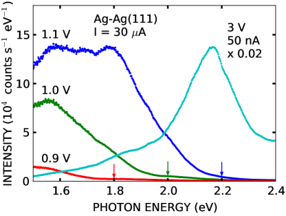
Figure 2 shows emission spectra from a Ag–Ag(111) junction recorded at low voltages – V, which were used to keep the photon energy of the more intense light below the detection threshold of eV 111 The quantum yields of the various emission components depend on the STM tip, the conductance, and the voltage. We recorded data for and light at and 0.8 V, respectively, with the same tip. Assuming isotropic emission the estimated quantum yield of light was at with this tip. The yields for and light at were lower by factors of and , respectively.. The spectra reveal significant emission, whose intensity drops towards (arrows). However, light at higher energies ( light) is also detected.
For further analysis the spectra recorded at a voltage were normalized by division with a reference spectrum recorded at an elevated bias while taking into account the expected linear cutoff of by a weighting factor Lambe and McCarthy (1976); Aguado and Kouwenhoven (2000); Blanter and Büttiker (2000):
| (1) |
This procedure removes the effect of the energy-dependent sensitivity of the detection setup Schneider et al. (2011). It also reduces the influence of the geometry of the junction on a nm scale Rendell and Scalapino (1981); Johansson et al. (1990); Berndt et al. (1991); Aizpurua et al. (2002). However, the position and shape of the plasmon resonance to some extent depend on the tip-sample distance Aizpurua et al. (2002). This distance cannot be made identical for measurements at low bias, where emission is discernible, and the higher voltages used to determine the shape of the plasmon resonance. As a result, the normalisation procedure used for Fig. 3 does not work well at the onset of the plasmon peak ( eV). We verified that the tip shape did not change during a set of measurements by recording reference spectra and STM images before and after.
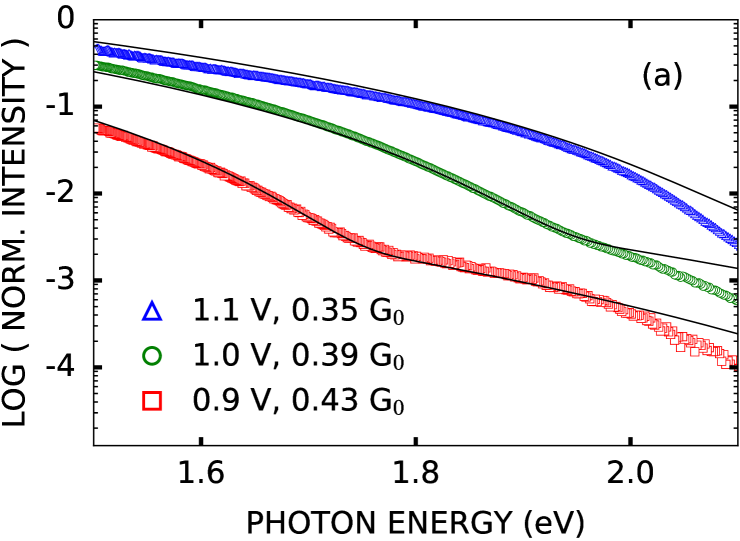
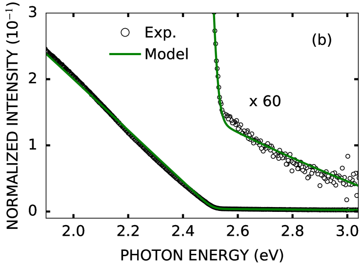
Figure 3(a) shows normalized data . The intensity, which is mainly due to light, smoothly drops towards the threshold for light, . Importantly, a clear change of slope is observed near the thresholds, which indicates that an additional radiative process becomes relevant. A change of slope is also clearly observed at the transition between the and spectral ranges shown in Fig. 3(b). The observed thresholds are difficult to reconcile with the scenario of Refs. Downes et al. (2002) and Buret et al. (2015), where heating of the electron gas by thousands of Kelvin was invoked to explain the emission of high-energy photons. That mechanism is not consistent with the present data from STM junctions.
To interpret the light emission up to photon energies of , we developed a model for higher-order scattering processes between electrons and the dynamic electric field of a plasmon-polariton resonance by combining the approaches of Refs. Xu et al., 2014, 2016; Kaasbjerg and Nitzan, 2015. The tip-induced plasmon of the STM junction is modelled as a damped LC circuit, which absorbs energy from tunneling electrons and emits photons at energies that may exceed . The electromagnetic enhancement due to the resonance is given by a Lorentzian , where is the frequency of the plasmon mode and is a damping parameter. Here denotes the effective impedance and the capacitance. The resonance describes both the emission enhancement as well as the effective interaction between the electrons. The coupling coefficient between the current and the plasmon is expressed as , where is the conductance and .
As detailed in the Supplemental Material, the rate of photon emission is governed by the enhancement factor and where is the shot noise spectral density of the current through non-interacting conductance channels with transmissions Aguado and Kouwenhoven (2000),
| (2) | |||||
| (3) | |||||
with , Fano factor , and where is the Bose-Einstein distribution. is some reference rate, which includes the detector efficiency and other experimentally unkown parameters.
The rate of the emission in the frequency range can at low temperature, , be expressed as
| (4) |
where in the integration domain. Correspondingly, the rate of the emission in the range is
| (5) |
Full expressions for the rates, in particular at finite temperatures, are provided in the Supplemental Material.
For illustration, Fig. 1 shows the overall spectra calculated assuming a featureless plasmon resonance, viz. At low temperature, the intensity rapidly drops at photon energies of as expected for processes involving electrons. The cutoff is less abrupt and shifts to higher energies at an elevated temperature of 500 K because of the broadened Fermi distributions of the electrodes. Note, that since we only have expressions for the light at and in the regime, we use always the zero temperature expression and extrapolated the curve beyond the regime, but we expect no significant changes in the energy range shown.
Next we use the model to fit experimental spectra. Figure 3(a) shows a comparison of experimental spectra (symbols) recorded at three voltages and the corresponding calculated results (lines) around the - threshold. The model reproduces the spectra fairly well assuming K. Deviations mainly occur at eV, where the normalization of the experimental data is less accurate.
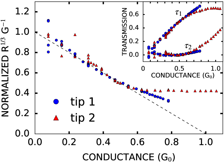
Figure 1 suggests that the - threshold should be more well-defined. This is indeed observed in the data [Fig. 3(b), circles] and reproduced by the model spectra (lines). In the model, a temperature of 55 K was found to lead to an acceptable fit, demonstrating that some heating does occurs. A further increase of the temperature would cause a shift of the kink and additional broadening. We conclude that the heating is orders of magnitude lower in our STM junctions than that previously invoked to interpret the emission of and light from electromigrated junctions Buret et al. (2015).
A fundamental prediction of our theory [cf. Eqs. (2)–(5)] is that the low-temperature emission in the regime scales with the conductance and Fano factor of a general multi-channel contact as
| (6) |
This suggests that the Fano factor can be inferred from the intensity as . In a simplified scenario of a single conductance channel with transmission , conductance , and Fano factor , a scaling previously confirmed for emission Kaasbjerg and Nitzan (2015) is therefore expected.
Figure 4 shows the measured photon intensity in the -light regime recorded with two different tips (symbols). The data have been scaled as in order to reflect the Fano factor for a single channel at vanishing conductance. In addition, the Fano factor for a single-channel contact is shown (dashed line). Up to conductance of , Fig. 4 shows a good match of the data and the simplified single-channel expectation. However, at higher conductance , significant deviations appear. To explain the discrepancy, we consider the opening of additional channels with increasing conductance which has previously been observed in Ag and noble metal contacts Scheer et al. (1998, 2001); Lü et al. (2013); Vardimon et al. (2013). In addition, they presumably are the reason for observed deviations of the yield from a simple behavior in Ag and Cu contacts Schneider et al. (2010); Burtzlaff et al. (2016).
The model can be made quantitative by assuming that at most two channels with transmissions and contribute. For the conductance and Fano factor we then have
| (7) |
respectively. Considering to be arbitrary functions of the conductance, we can extract their conductance dependencies from the intensities in Fig. 4 without additional fitting parameters. The result for the variation of the two channel transmissions with the overall conductance is shown in the inset of Fig 4. The extracted transmission coefficients clearly support the opening of an additional conductance channel at –. The intensity for both tips is thus in full accordance with the model invoking two conductance channels without involving any heating. Hence, the light emission from the STM can be explained by coherent plasmon-mediated multi-electron processes.
In summary, we have analyzed the emission of , , and light from atomic scale contacts in a STM. Characteristic features of the spectra, the relative intensities, and the scaling with the conductance are consistently explained in terms of higher-order electron-plasmon interaction. Our results exclude high electron temperatures as being the reason of the overbias light emission in the present STM experiments. Rather, they suggest that it is promising to extend the mesoscopic transport formulation presented here to more complex situations involving, e.g., molecules in the transport path Schneider et al. (2012); Reecht et al. (2014); Doppagne et al. (2017) or complex interacting plasmon resonances. In antenna structures maximizing the electron-plasmon interaction Parzefall et al. (2015); Bigourdan et al. (2016) higher-order effects may be further enhanced. Another interesting direction will be to consider pulsed bias voltages leading to correlated photon emission.
Acknowledgements.
We thank Tomáš Novotný and Juan-Carlos Cuevas for discussions. K.K. acknowledges support from the European Union’s Horizon 2020 research and innovation programme under the Marie Sklodowska-Curie grant agreement no. 713683 (COFUNDfellowsDTU). G.R., F.X., and W.B. acknowledge financial support by the DFG through SFB 767.References
- Lambe and McCarthy (1976) J. Lambe and S. L. McCarthy, Phys. Rev. Lett. 37, 923 (1976).
- Berndt et al. (1993) R. Berndt, J. K. Gimzewski, and P. Johansson, Phys. Rev. Lett. 71, 3493 (1993).
- Atay et al. (2004) T. Atay, J.-H. Song, and A. V. Nurmikko, Nano Lett. 4, 1627 (2004).
- Romero et al. (2006) I. Romero, J. Aizpurua, G. W. Bryant, and F. J. García De Abajo, Opt. Express 14, 9988 (2006).
- Savage et al. (2012) K. J. Savage, M. M. Hawkeye, R. Esteban, A. G. Borisov, J. Aizpurua, and J. J. Baumberg, Nature 491, 574 (2012).
- Marinica et al. (2015) D. C. Marinica, M. Zapata, P. Nordlander, A. K. Kazansky, P. M. Echenique, J. Aizpurua, and A. G. Borisov, Sci. Adv. 1, 1 (2015).
- Vardi et al. (2016) Y. Vardi, E. Cohen-Hoshen, G. Shalem, and I. Bar-Joseph, Nano Lett. 16, 748 (2016).
- Möller et al. (1991) R. Möller, U. Albrecht, J. Boneberg, B. Koslowski, P. Leiderer, and K. Dransfeld, J. Vac. Sci. Technol. B 9, 506 (1991).
- Völcker et al. (1991) M. Völcker, W. Krieger, and H. Walther, Phys. Rev. Lett. 66, 1717 (1991).
- Guhr et al. (2007) D. C. Guhr, D. Rettinger, J. Boneberg, A. Erbe, P. Leiderer, and E. Scheer, Phys. Rev. Lett. 99, 086801 (2007).
- Berndt et al. (1991) R. Berndt, J. K. Gimzewski, and P. Johansson, Phys. Rev. Lett. 67, 3796 (1991).
- Schneider et al. (2010) N. L. Schneider, G. Schull, and R. Berndt, Phys. Rev. Lett. 105, 026601 (2010).
- Le Moal et al. (2016) E. Le Moal, S. Marguet, D. Canneson, B. Rogez, E. Boer-Duchemin, G. Dujardin, T. V. Teperik, D.-C. Marinica, and A. G. Borisov, Phys. Rev. B 93, 035418 (2016).
- Kuhnke et al. (2017) K. Kuhnke, C. Große, P. Merino, and K. Kern, Chem. Rev. 117, 5174 (2017).
- Bharadwaj et al. (2011) P. Bharadwaj, A. Bouhelier, and L. Novotny, Phys. Rev. Lett. 106, 226802 (2011).
- Kern et al. (2015) J. Kern, R. Kullock, J. C. Prangsma, M. Emmerling, M. Kamp, and B. Hecht, Nat. Photonics 9, 582 (2015).
- Pechou et al. (1998) R. Pechou, R. Coratger, F. Ajustron, and J. Beauvillain, Appl. Phys. Lett. 72, 671 (1998).
- Downes et al. (2002) A. Downes, P. Dumas, and M. E. Welland, Appl. Phys. Lett. 81, 1252 (2002).
- Hoffmann et al. (2003) G. Hoffmann, R. Berndt, and P. Johansson, Phys. Rev. Lett. 90, 046803 (2003).
- Dong et al. (2004) Z.-C. Dong, X.-L. Guo, A. S. Trifonov, P. S. Dorozhkin, K. Miki, K. Kimura, S. Yokoyama, and S. Mashiko, Phys. Rev. Lett. 92, 086801 (2004).
- Uemura et al. (2007) T. Uemura, M. Furumoto, T. Nakano, M. Akai-Kasaya, A. Saito, M. Aono, and Y. Kuwahara, Chem. Phys. Lett. 448, 232 (2007).
- Schull et al. (2009) G. Schull, N. Néel, P. Johansson, and R. Berndt, Phys. Rev. Lett. 102, 057401 (2009).
- Dong et al. (2010) Z.-C. Dong, X. L. Zhang, H. Y. Gao, Y. Luo, C. Zhang, L. G. Chen, R. Zhang, X. Tao, Y. Zhang, J. L. Yang, and J. G. Hou, Nat. Photonics 4, 50 (2010).
- Fujiki et al. (2011) A. Fujiki, Y. Miyake, Y. Oshikane, M. Akai-Kasaya, A. Saito, and Y. Kuwahara, Nanoscale Res. Lett. 6, 1 (2011).
- Schneider et al. (2013) N. L. Schneider, P. Johansson, and R. Berndt, Phys. Rev. B 87, 045409 (2013).
- Xu et al. (2014) F. Xu, C. Holmqvist, and W. Belzig, Phys. Rev. Lett. 113, 066801 (2014).
- Xu et al. (2016) F. Xu, C. Holmqvist, G. Rastelli, and W. Belzig, Phys. Rev. B 94, 245111 (2016).
- Kaasbjerg and Nitzan (2015) K. Kaasbjerg and A. Nitzan, Phys. Rev. Lett. 114, 126803 (2015).
- Buret et al. (2015) M. Buret, A. V. Uskov, J. Dellinger, N. Cazier, M.-M. Mennemanteuil, J. Berthelot, I. V. Smetanin, I. E. Protsenko, G. Colas-des Francs, and A. Bouhelier, Nano Lett. 15, 5811 (2015).
- Castellanos-Gomez et al. (2012) A. Castellanos-Gomez, G. Rubio-Bollinger, M. Garnica, S. Barja, A. L. Vázquez de Parga, R. Miranda, and N. Agraït, Ultramicroscopy 122, 1 (2012).
- Hoffmann et al. (2002) G. Hoffmann, J. Kröger, and R. Berndt, Rev. Sci. Instrum. 73, 305 (2002).
- Note (1) The quantum yields of the various emission components depend on the STM tip, the conductance, and the voltage. We recorded data for and light at and 0.8 V, respectively, with the same tip. Assuming isotropic emission the estimated quantum yield of light was at with this tip. The yields for and light at were lower by factors of and , respectively.
- Aguado and Kouwenhoven (2000) R. Aguado and L. P. Kouwenhoven, Phys. Rev. Lett. 84, 1986 (2000).
- Blanter and Büttiker (2000) Y. M. Blanter and M. Büttiker, Phys. Rep. 336, 1 (2000).
- Schneider et al. (2011) N. L. Schneider, F. Matino, G. Schull, S. Gabutti, M. Mayor, and R. Berndt, Phys. Rev. B 84, 153403 (2011).
- Rendell and Scalapino (1981) R. W. Rendell and D. J. Scalapino, Phys. Rev. B 24, 3276 (1981).
- Johansson et al. (1990) P. Johansson, R. Monreal, and P. Apell, Phys. Rev. B 42, 9210 (1990).
- Aizpurua et al. (2002) J. Aizpurua, G. Hoffmann, S. P. Apell, and R. Berndt, Phys. Rev. Lett. 89, 156803 (2002).
- Scheer et al. (1998) E. Scheer, N. Agraït, J. C. Cuevas, A. L. Yeyati, B. Ludoph, A. Martín-Rodero, G. R. Bollinger, J. M. van Ruitenbeek, and C. Urbina, Nature 394, 154 (1998).
- Scheer et al. (2001) E. Scheer, W. Belzig, Y. Naveh, M. H. Devoret, D. Esteve, and C. Urbina, Phys. Rev. Lett. 86, 284 (2001).
- Lü et al. (2013) J.-T. Lü, R. B. Christensen, and M. Brandbyge, Phys. Rev. B 88, 045413 (2013).
- Vardimon et al. (2013) R. Vardimon, M. Klionsky, and O. Tal, Phys. Rev. B 88, 161404 (2013).
- Burtzlaff et al. (2016) A. Burtzlaff, N. L. Schneider, A. Weismann, and R. Berndt, Surf. Sci. 643, 10 (2016).
- Schneider et al. (2012) N. L. Schneider, J. T. Lü, M. Brandbyge, and R. Berndt, Phys. Rev. Lett. 109, 186601 (2012).
- Reecht et al. (2014) G. Reecht, F. Scheurer, V. Speisser, Y. J. Dappe, F. Mathevet, and G. Schull, Phys. Rev. Lett. 112, 047403 (2014).
- Doppagne et al. (2017) B. Doppagne, M. C. Chong, E. Lorchat, S. Berciaud, M. Romeo, H. Bulou, A. Boeglin, F. Scheurer, and G. Schull, Phys. Rev. Lett. 118, 127401 (2017).
- Parzefall et al. (2015) M. Parzefall, P. Bharadwaj, A. Jain, T. Taniguchi, K. Watanabe, and L. Novotny, Nat. Nanotechnol. 10, 1058 (2015).
- Bigourdan et al. (2016) F. Bigourdan, J.-P. Hugonin, F. Marquier, C. Sauvan, and J.-J. Greffet, Phys. Rev. Lett. 116, 106803 (2016).