Quantum interferometry with a g-factor-tunable spin qubit
Abstract
We study quantum interference effects of a qubit whose energy levels are continuously modulated. The qubit is formed by an impurity electron spin in a silicon tunneling field-effect transistor, and it is read out by spin blockade in a double-dot configuration. The qubit energy levels are modulated via its gate-voltage-dependent -factors, with either rectangular, sinusoidal, or ramp radio-frequency waves. The energy-modulated qubit is probed by the electron spin resonance. Our results demonstrate the potential of spin qubit interferometry implemented in a silicon device and operated at a relatively high temperature.
pacs:
73.63.Kv, 73.23.Hk, 76.30.-vIntroduction.—Sensitive measurement techniques are based on the interference of waves. The most striking illustration is the recent use of interferometry for the detection of gravitational waves Abbott et al. (2016). If in place of classical electromagnetic waves one can use the wave functions of quantum objects, such techniques can be called quantum interferometry. This was studied not only for conventional small quantum objects Suda (2006); Braun et al. (2018), but also for large organic molecules Gerlich et al. (2011); Hornberger et al. (2012) and micrometer-size superconducting circuits Oliver et al. (2005); Sillanpää et al. (2006); Shevchenko et al. (2010); see also a recent review article [Degen et al., 2017] for different realizations and applications in quantum sensing. Since it is difficult to maintain a coherent superposition of charge states, it might be more beneficial to use instead the spin degree of freedom Morton et al. (2011). Interestingly, silicon, the second most abundant element in the Earth’s crust and the base of modern electronics, is an ideal environment for spins in the solid state Zwanenburg et al. (2013). In this work, we will explore how to use a single-spin silicon-based qubit for quantum interferometry.
Among other characteristics, for quantum engineering it is important to have qubits which are “hot, dense, and coherent” Vandersypen et al. (2017). In this context, “hot” means working in the technologically less challenging few-Kelvin regime rather than being cooled down to the milli-Kelvin domain. “Dense” refers to the possibility to achieve high density of quantum dots or donors in semiconductors. Another benefit of this platform is its compatibility with the well-developed complementary-metal-oxide-semiconductor (CMOS) technology. Even more, it has been shown Maurand et al. (2016); Gonzalez-Zalba et al. (2016); Ono et al. (2017) that transistors can behave as quantum dots, in which either charge or spin qubits are realized.
Quantum systems can be modulated by signals of different shapes, such as sinusoidal and square-wave signals. The latter allows one to rapidly change a qubit state from one to another, which we can refer to as latching modulation of qubit states Silveri et al. (2015, 2017). If this is done with a period longer than the coherence time, then the response has two separate peaks, situated at the two resonance frequencies corresponding to the two states. Increasing the modulation frequency, the coherent response is displayed as an averaged signal, situated at a frequency between the two resonance frequencies mentioned above, which is known as motional narrowing. Both motional averaging and narrowing are known in NMR systems and recently also studied in superconducting systems Li et al. (2013); Pan et al. (2017). In this way, by changing the modulation frequency, namely its ratio to the coherence rate, one can observe the transition between classical (incoherent) and quantum (coherent) regimes, as in Refs. Fink et al. (2010); Fedorov et al. (2011); Li et al. (2013); Pietikäinen et al. (2017).
In this work, we focus on the time-ensemble behavior of a spin- qubit and study the effect of continuously modulating the qubit energy. In this way, we explore the motional averaging not only for the symmetric latching modulation (which was previously demonstrated in superconducting qubits Li et al. (2013); Silveri et al. (2015, 2017)), but also in the asymmetric regime, where dwelling in one state is longer than in the other state. A square-wave modulation with variable duty ratio shows weighted motional averaging. At low modulation frequency, this is visualized, in the frequency dependence, by two peaks (with weighted height and width); while at high modulation frequency there is only one averaged peak. We also demonstrate the sinusoidal energy modulation of the spin qubit and show the Landau-Zener-Stückelberg-Majorana (LZSM) interference of the spin resonance signal. This is the first demonstration of LZSM interference where the temperature is much higher than the photon energy of the sinusoidal modulation frequency. For realizations of the low-temperature LZSM interference in quantum-dot systems see Refs. Stehlik et al. (2012); Forster et al. (2014); Stehlik et al. (2016); Korkusinski et al. (2017); Bogan et al. (2018); Chatterjee et al. (2018); Pasek et al. (2018); Koski et al. (2018).
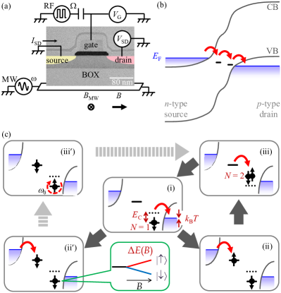
Device and measurement.—We used a spin qubit device based on a short-channel tunneling field-effect transistor, TFET Ionescu and Riel (2011), with the implanted deep impurity, Fig. 1(a) Mori et al. (2014, 2015a, 2015b, 2017); Ono et al. (2019). The device is essentially a gate-tunable PIN diode (a diode with an undoped intrinsic semiconductor region between a -type semiconductor and an -type semiconductor region). The ion implantations created coupled Al-N impurity pairs in silicon Weber et al. (1980); Sauer et al. (1984); Modavis and Hall (1990); Iizuka and Nakayama (2015). For an appropriate channel length, a three-step tunneling from the -type source electrode to the -type drain electrode occurs via two localized states in the channel, Fig. 1(b). The PIN structure allows tunneling via the localized states of a deep impurity and a shallow impurity Sup ; Ono et al. (2019).
Spin blockade and ESR.—The device has two localized states, which behave as a double quantum dot device, where the current is defined by single-electron transport van der Wiel et al. (2002). Under an appropriate source voltage and gate voltage , the device shows spin blockade (SB) Ono et al. (2002). At the electron spin resonance (ESR) for one of the spins in the double dot, the source-drain current increases due to the lifting of the spin blockade Fig. 1(c) Koppens et al. (2006); Maurand et al. (2016). Note that the large on-site Coulomb energy and strong confinement of these impurities allow a spin-qubit operation with a reasonable coherence time ( s) at relatively high temperatures and low magnetic fields Pla et al. (2012). Changing the gate voltage within the spin blockade region changes the -factor by about due to the Stark effect Rahman et al. (2009).
We describe our spin qubit device as a two-level system with the pseudo-spin Hamiltonian . The longitudinal part is defined by the Zeeman splitting, . The time-dependent gate voltage changes the -factor by a small value and we have , where the amplitude ; represents the ESR frequency. In this work, we consider three types of signals Sup : a sinusoidal modulation, , a latching modulation, given by
| (1) |
where is the duty-cycle ratio, and a ramp modulation, given by the fractional part in . Note that for a symmetric latching modulation, with , from Eq. (1), we have . In addition, the transverse part of the Hamiltonian is defined by the MW voltage applied to the substrate, with amplitude and circular frequency . The modulation is assumed to be slow, i.e. .
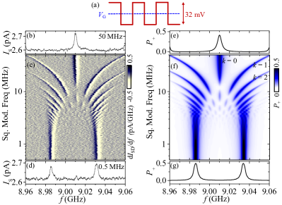
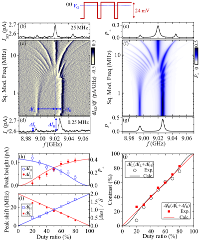
Square-wave modulation.—In figures 2 and 3 we present the results of our measurements and calculations for symmetric and asymmetric square-wave modulation signals. The left panel focuses on the source-drain current , showing the current derivative, , in its main panel. The right panel presents the corresponding theoretical predictions for the qubit upper-level occupation.
By adding a square-wave MHz modulation signal to the gate [Fig. 2(a)], the gate voltage, i.e. -factor, can be switched between two values, as described by Eq. (1). Figure 2(d) shows at V and square wave of frequency MHz and amplitude mV. Due to the slow measurement with a time constant (that shows how fast the measured current changes) s, we observe the two ESR peaks with two different -factors for V and V, respectively. By increasing the modulation frequency, the ESR peaks show a characteristic interference pattern and eventually a strong (main) peak appears with weak sideband peaks [Fig. 2(b)]. The strong single peak at GHz [Fig. 2(b)] is a result of motional averaging of the two peaks for the slow modulation [Fig. 2(d)]. A similar pattern was observed for latching modulation of the energy of a superconducting qubit in Ref. Silveri et al. (2015). Changing the modulation amplitude shows a similar behavior with a similar crossover frequency Sup .
In order to describe the system, we solve the Bloch equations with the above Hamiltonian. We assume that and after a rotating-wave approximation
| (2) |
where . Details of the calculations are presented in Sup , cf. Refs. Shevchenko et al. (2005); Ivakhnenko et al. (2018). As a result, the upper-level occupation probability is readily obtained from the stationary solution of the Bloch equations:
| (3) |
where , which can be interpreted as the dressed qubit gap, modulated by the function . The relaxation and decoherence rates are denoted as and , respectively. In particular, for rectangular modulating system with duty-cycle ratio , we obtain:
| (4) |
We can interpret the effective Hamiltonian (2) as follows. The microwave drive dresses the two-level system resulting in an energy level difference ; when this is matched to the -photon energy of the rf-signal, the dressed qubit is resonantly excited. Indeed, the upper-level population in Eq. (3) has maxima at Childress and McIntyre (2010); Li et al. (2013). With Eq. (3) we generated the interferograms in the right panels of Figs. 2-4. Sup In particular, for Fig. 2 we used Eq. (4) with .
Asymmetric modulation.—Changing the duty ratio (ratio of the low signal duration to the period; for the previous square wave the duty ratio was %), shows both asymmetric modulation and weighted motional average, as demonstrated in Fig. 3. Because the modulation voltage is added through the block capacitor, the areas of the signal curves below and above the average gate voltage are equal, as shown in Fig. 3(a). Figure 3(d) shows the ESR under slow modulation of the square-wave signal with a % duty ratio. The two ESR peak heights are different, reflecting the duty ratio. For fast modulation, the main peak appears at the weighted averaged frequency [Fig. 3(b)].
We repeat similar measurements with various duty ratios (from to ). In figure 3(h) we plot the heights of the two ESR peaks at lowest modulation frequency. For each duty ratio, we also plot distances between the above two peak positions and the motional averaged main peak position at the highest modulation frequency [Fig. 3(i)]. Both of the peak heights and distances reflect the duty ratios. The ratio of the peak heights and the frequency distances are plotted in Fig. 3(j), and show the motional-averaged main peaks, which indeed appear at the weighted average frequency. The deviations from linear dependencies in these plots, especially for the duty ratio of , are due to the gate-voltage dependence of the ESR peak height. More detailed measurements for each duty ratio are shown in Sup .
We note here the following interesting features of the weighted motional averaging. The rectangular-pulse modulation places the qubit in one of the two allowed positions, and the low-frequency characteristics reflect the weighted time spent in those two states. For high , the principal ESR line is situated in-between the two qubit states, the position of which is independent of the duty ratio. A counter-intuitive aspect is that the position of this line does not relate to any of the two qubit states, and thus is referred to as “motional averaging” Li et al. (2013). Details of calculations are presented in Sup . There, it is shown that the frequency shifts are the following: and , while the peak heights are nonlinear functions of . These formulas are plotted with solid lines in Fig. 3(h-j).
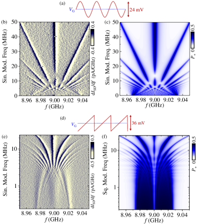
Sinusoidal and ramp modulation.—Figure 4(b,c) shows the effect of the sinusoidal modulation that produces the Landau-Zener-Stückelberg-Majorana interference patten. The modulation amplitude dependence with fixed modulation frequency shows the radio-frequency-wave assisted side bands Sup . In the case of a sinusoidal modulation, the dressed energy gap is given by the Bessel function of the first kind .Childress and McIntyre (2010) Then, with Eq. (3) we plot Fig. 4(c). Ramp-wave modulations are shown in Fig. 4(e,f). An inverse ramp waveform gives identical results Sup . We note that at low modulation frequency and low detuning the agreement is rather qualitative, which might be due to the rotating-wave approximation.
Discussion.—We have demonstrated that under certain conditions, an impurity in a field-effect transistor behaves as a single-spin qubit which displays coherent phenomena, such as Landau-Zener-Stückelberg-Majorana interference and motional averaging. The spin-qubit device is based on a short-channel TFET in which, for an appropriate channel length, a three-step tunneling from the -type source electrode to the -type drain electrode occurs via two localized states in the channel. These localized states (in a deep impurity and a shallow impurity) form a double quantum dot in which the spin qubit is formed in the spin-blockade regime. The -factor of the spin can be tuned by the gate voltage, which enables the fast modulation of the qubit energy. We demonstrated coherent control by modulating the qubit energy with various continuous waveforms. In particular, when modulated by asymmetric rectangular pulses with duty ratio , we observed interferograms, which we refer to as weighted motional averaging. At low frequency, this displays -weighted peaks which, at higher frequency, merge into one peak. To conclude, we summarize the advantages of the silicon single-spin interferometers: they operate at relatively high temperature (K), the -factor is controlled by the gate voltage (, important for selectivity of measurements), the relaxation times are large, the fabrication is based on the well-developed techniques for silicon, such as CMOS, and they can be manipulated into the ESR and Pauli spin blockade regimes.
Acknowledgements.
We thank K. Ishibashi for discussions and M. Cirio and N. Lambert for critically reading the manuscript. This work was supported by JSPS KAKENHI Grant No. 15H04000, 17H01276. F.N. is supported in part by the MURI Center for Dynamic Magneto-Optics via the Air Force Office of Scientific Research (AFOSR) (FA9550-14-1-0040), Army Research Office (ARO) (Grant No. W911NF-18-1-0358), Asian Office of Aerospace Research and Development (AOARD) (Grant No. FA2386-18-1-4045), Japan Science and Technology Agency (JST) (Q-LEAP program and CREST Grant No. JPMJCR1676), Japan Society for the Promotion of Science (JSPS) (JSPS-RFBR Grant No. 17-52-50023 and JSPS-FWO Grant No. VS.059.18N), RIKEN-AIST Challenge Research Fund, and the John Templeton Foundation.References
- Abbott et al. (2016) B. P. Abbott et al. (LIGO Scientific Collaboration and Virgo Collaboration), “Observation of gravitational waves from a binary black hole merger,” Phys. Rev. Lett. 116, 061102 (2016).
- Suda (2006) M. Suda, Quantum Interferometry in Phase Space (Springer, Berlin Heidelberg New York, 2006).
- Braun et al. (2018) D. Braun, G. Adesso, F. Benatti, R. Floreanini, U. Marzolino, M. W. Mitchell, and S. Pirandola, “Quantum-enhanced measurements without entanglement,” Rev. Mod. Phys. 90, 035006 (2018).
- Gerlich et al. (2011) S. Gerlich, S. Eibenberger, M. Tomandl, S. Nimmrichter, K. Hornberger, P. J. Fagan, J. Tüxen, M. Mayor, and M. Arndt, “Quantum interference of large organic molecules,” Nat. Comm. 2, 263 (2011).
- Hornberger et al. (2012) K. Hornberger, S. Gerlich, P. Haslinger, S. Nimmrichter, and M. Arndt, “Colloquium: Quantum interference of clusters and molecules,” Rev. Mod. Phys. 84, 157–173 (2012).
- Oliver et al. (2005) W. D. Oliver, Y. Yu, J. C. Lee, K. K. Berggren, L. S. Levitov, and T. P. Orlando, “Mach-Zehnder interferometry in a strongly driven superconducting qubit,” Science 310, 1653–1657 (2005).
- Sillanpää et al. (2006) M. Sillanpää, T. Lehtinen, A. Paila, Y. Makhlin, and P. Hakonen, “Continuous-time monitoring of Landau-Zener interference in a Cooper-pair box,” Phys. Rev. Lett. 96, 187002 (2006).
- Shevchenko et al. (2010) S. N. Shevchenko, S. Ashhab, and F. Nori, “Landau-Zener-Stückelberg interferometry,” Phys. Rep. 492, 1–30 (2010).
- Degen et al. (2017) C. L. Degen, F. Reinhard, and P. Cappellaro, “Quantum sensing,” Rev. Mod. Phys. 89, 035002 (2017).
- Morton et al. (2011) J. J. L. Morton, D. R. McCamey, M. A. Eriksson, and S. A. Lyon, “Embracing the quantum limit in silicon computing,” Nature 479, 345–353 (2011).
- Zwanenburg et al. (2013) F. A. Zwanenburg, A. S. Dzurak, A. Morello, M. Y. Simmons, L. C. L. Hollenberg, G. Klimeck, S. Rogge, S. N. Coppersmith, and M. A. Eriksson, “Silicon quantum electronics,” Rev. Mod. Phys. 85, 961–1019 (2013).
- Vandersypen et al. (2017) L. M. K. Vandersypen, H. Bluhm, J. S. Clarke, A. S. Dzurak, R. Ishihara, A. Morello, D. J. Reilly, L. R. Schreiber, and M. Veldhorst, “Interfacing spin qubits in quantum dots and donors–hot, dense, and coherent,” npj Quantum Info. 3, 34 (2017).
- Maurand et al. (2016) R. Maurand, X. Jehl, D. Kotekar-Patil, A. Corna, H. Bohuslavskyi, R. Laviéville, L. Hutin, S. Barraud, M. Vinet, M. Sanquer, and S. De Franceschi, “A CMOS silicon spin qubit,” Nat. Comm. 7, 13575 (2016).
- Gonzalez-Zalba et al. (2016) M. F. Gonzalez-Zalba, S. N. Shevchenko, S. Barraud, J. R. Johansson, A. J. Ferguson, F. Nori, and A. C. Betz, “Gate-sensing coherent charge oscillations in a silicon field-effect transistor,” Nano Lett. 16, 1614–1619 (2016).
- Ono et al. (2017) K. Ono, G. Giavaras, T. Tanamoto, T. Ohguro, X. Hu, and F. Nori, “Hole spin resonance and spin-orbit coupling in a silicon metal-oxide-semiconductor field-effect transistor,” Phys. Rev. Lett. 119, 156802 (2017).
- Silveri et al. (2015) M. P. Silveri, K. S. Kumar, J. Tuorila, J. Li, A. Vepsäläinen, E. V. Thuneberg, and G. S. Paraoanu, “Stückelberg interference in a superconducting qubit under periodic latching modulation,” New J. Phys. 17, 043058 (2015).
- Silveri et al. (2017) M. P. Silveri, J. A. Tuorila, E. V. Thuneberg, and G. S. Paraoanu, “Quantum systems under frequency modulation,” Rep. Prog. Phys. 80, 056002 (2017).
- Li et al. (2013) J. Li, M. P. Silveri, K. S. Kumar, J.-M. Pirkkalainen, A. Vepsäläinen, W. C. Chien, J. Tuorila, M. A. Sillanpää, P. J. Hakonen, E. V. Thuneberg, and G. S. Paraoanu, “Motional averaging in a superconducting qubit,” Nat. Comm. 4, 1420 (2013).
- Pan et al. (2017) J. Pan, Y. Fan, Y. Li, X. Dai, X. Wei, Y. Lu, C. Cao, L. Kang, W. Xu, J. Chen, G. Sun, and P. Wu, “Dynamically modulated Autler-Townes effect in a transmon qubit,” Phys. Rev. B 96, 024502 (2017).
- Fink et al. (2010) J. M. Fink, L. Steffen, P. Studer, L. S. Bishop, M. Baur, R. Bianchetti, D. Bozyigit, C. Lang, S. Filipp, P. J. Leek, and A. Wallraff, “Quantum-to-classical transition in cavity quantum electrodynamics,” Phys. Rev. Lett. 105, 163601 (2010).
- Fedorov et al. (2011) A. Fedorov, P. Macha, A. K. Feofanov, C. J. P. M. Harmans, and J. E. Mooij, “Tuned transition from quantum to classical for macroscopic quantum states,” Phys. Rev. Lett. 106, 170404 (2011).
- Pietikäinen et al. (2017) I. Pietikäinen, S. Danilin, K. S. Kumar, A. Vepsäläinen, D. S. Golubev, J. Tuorila, and G. S. Paraoanu, “Observation of the Bloch-Siegert shift in a driven quantum-to-classical transition,” Phys. Rev. B 96, 020501 (2017).
- Stehlik et al. (2012) J. Stehlik, Y. Dovzhenko, J. R. Petta, J. R. Johansson, F. Nori, H. Lu, and A. C. Gossard, “Landau-Zener-Stückelberg interferometry of a single electron charge qubit,” Phys. Rev. B 86, 121303 (2012).
- Forster et al. (2014) F. Forster, G. Petersen, S. Manus, P. Hänggi, D. Schuh, W. Wegscheider, S. Kohler, and S. Ludwig, “Characterization of qubit dephasing by Landau-Zener-Stückelberg-Majorana interferometry,” Phys. Rev. Lett. 112, 116803 (2014).
- Stehlik et al. (2016) J. Stehlik, M. Z. Maialle, M. H. Degani, and J. R. Petta, “Role of multilevel Landau-Zener interference in extreme harmonic generation,” Phys. Rev. B 94, 075307 (2016).
- Korkusinski et al. (2017) M. Korkusinski, S. A. Studenikin, G. Aers, G. Granger, A. Kam, and A. S. Sachrajda, “Landau-Zener-Stückelberg interferometry in quantum dots with fast rise times: Evidence for coherent phonon driving,” Phys. Rev. Lett. 118, 067701 (2017).
- Bogan et al. (2018) A. Bogan, S. Studenikin, M. Korkusinski, L. Gaudreau, P. Zawadzki, A. S. Sachrajda, L. Tracy, J. Reno, and T. Hargett, “Landau-Zener-Stückelberg-Majorana interferometry of a single hole,” Phys. Rev. Lett. 120, 207701 (2018).
- Chatterjee et al. (2018) A. Chatterjee, S. N. Shevchenko, S. Barraud, R. M. Otxoa, F. Nori, J. J. L. Morton, and M. F. Gonzalez-Zalba, “A silicon-based single-electron interferometer coupled to a fermionic sea,” Phys. Rev. B 97, 045405 (2018).
- Pasek et al. (2018) W. J. Pasek, M. Z. Maialle, and M. H. Degani, “Application of the Landau-Zener-Stückelberg-Majorana dynamics to the electrically driven flip of a hole spin,” Phys. Rev. B 97, 115417 (2018).
- Koski et al. (2018) J. V. Koski, A. J. Landig, A. Palyi, P. Scarlino, C. Reichl, W. Wegscheider, G. Burkard, A. Wallraff, K. Ensslin, and T. Ihn, “Floquet spectroscopy of a strongly driven quantum dot charge qubit with a microwave resonator,” Phys. Rev. Lett. 121, 043603 (2018).
- Ionescu and Riel (2011) A. M. Ionescu and H. Riel, “Tunnel field-effect transistors as energy-efficient electronic switches,” Nature 479, 329–337 (2011).
- Mori et al. (2014) T. Mori, Y. Morita, N. Miyata, S. Migita, K. Fukuda, M. Masahara, T. Yasuda, and H. Ota, “Band-to-band tunneling current enhancement utilizing isoelectronic trap and its application to TFETs,” in VLSI Technology (VLSI-Technology): Digest of Technical Papers, 2014 Symposium on (IEEE, 2014) pp. 1–2.
- Mori et al. (2015a) T. Mori, W. Mizubayashi, Y. Morita, S. Migita, K. Fukuda, N. Miyata, T. Yasuda, M. Masahara, and H. Ota, “Effect of hot implantation on ON-current enhancement utilizing isoelectronic trap in Si-based tunnel field-effect transistors,” Appl. Phys. Expr. 8, 036503 (2015a).
- Mori et al. (2015b) T. Mori, Y. Morita, N. Miyata, S. Migita, K. Fukuda, W. Mizubayashi, M. Masahara, T. Yasuda, and H. Ota, “Study of tunneling transport in Si-based tunnel field-effect transistors with ON current enhancement utilizing isoelectronic trap,” Appl. Phys. Lett. 106, 083501 (2015b).
- Mori et al. (2017) T. Mori, S. Iizuka, and T. Nakayama, “Material engineering for silicon tunnel field-effect transistors: isoelectronic trap technology,” MRS Communications 7, 541–550 (2017).
- Ono et al. (2019) K. Ono, T. Mori, and S. Moriyama, “High-temperature operation of a silicon qubit,” Sci. Rep. 9, 469 (2019).
- Weber et al. (1980) J. Weber, W. Schmid, and R. Sauer, “Localized exciton bound to an isoelectronic trap in silicon,” Phys. Rev. B 21, 2401 (1980).
- Sauer et al. (1984) R. Sauer, J. Weber, and W. Zulehner, “Nitrogen in silicon: Towards the identification of the 1.1223-eV (A, B, C) photoluminescence lines,” Appl. Phys. Lett. 44, 440–442 (1984).
- Modavis and Hall (1990) R. A. Modavis and D. G. Hall, “Aluminum-nitrogen isoelectronic trap in silicon,” J. Appl. Phys. 67, 545–547 (1990).
- Iizuka and Nakayama (2015) S. Iizuka and T. Nakayama, “First-principles calculation of electronic properties of isoelectronic impurity complexes in Si,” Appl. Phys. Expr. 8, 081301 (2015).
- (41) See Supplemental Material at [URL will be inserted by publisher] .
- van der Wiel et al. (2002) W. G. van der Wiel, S. De Franceschi, J. M. Elzerman, T. Fujisawa, S. Tarucha, and L. P. Kouwenhoven, “Electron transport through double quantum dots,” Rev. Mod. Phys. 75, 1–22 (2002).
- Ono et al. (2002) K. Ono, D. Austing, Y. Tokura, and S. Tarucha, “Current rectification by Pauli exclusion in a weakly coupled double quantum dot system,” Science 297, 1313–1317 (2002).
- Koppens et al. (2006) F. H. L. Koppens, C. Buizert, K.-J. Tielrooij, I. T. Vink, K. C. Nowack, T. Meunier, L. P. Kouwenhoven, and L. M. K. Vandersypen, “Driven coherent oscillations of a single electron spin in a quantum dot,” Nature 442, 766–771 (2006).
- Pla et al. (2012) J. J. Pla, K. Y. Tan, J. P. Dehollain, W. H. Lim, J. J. L. Morton, D. N. Jamieson, A. S. Dzurak, and A. Morello, “A single-atom electron spin qubit in silicon,” Nature 489, 541–545 (2012).
- Rahman et al. (2009) R. Rahman, S. H. Park, T. B. Boykin, G. Klimeck, S. Rogge, and L. C. L. Hollenberg, “Gate-induced g-factor control and dimensional transition for donors in multivalley semiconductors,” Phys. Rev. B 80, 155301 (2009).
- Shevchenko et al. (2005) S. N. Shevchenko, A. S. Kiyko, A. N. Omelyanchouk, and W. Krech, “Dynamic behavior of Josephson-junction qubits: crossover between Rabi oscillations and Landau-Zener transitions,” Low Temp. Phys. 31, 569–576 (2005).
- Ivakhnenko et al. (2018) O. V. Ivakhnenko, S. N. Shevchenko, and F. Nori, “Simulating quantum dynamical phenomena using classical oscillators: Landau-Zener-Stückelberg-Majorana interferometry, latching modulation, and motional averaging,” Sci. Rep. 8, 12218 (2018).
- Childress and McIntyre (2010) L. Childress and J. McIntyre, “Multifrequency spin resonance in diamond,” Phys. Rev. A 82, 033839 (2010).