Topologically non-trivial valley states in bilayer graphene quantum point contacts
Abstract
We present measurements of quantized conductance in electrostatically induced quantum point contacts in bilayer graphene. The application of a perpendicular magnetic field leads to an intricate pattern of lifted and restored degeneracies with increasing field: at zero magnetic field the degeneracy of quantized one-dimensional subbands is four, because of a twofold spin and a twofold valley degeneracy. By switching on the magnetic field, the valley degeneracy is lifted. Due to the Berry curvature states from different valleys split linearly in magnetic field. In the quantum Hall regime fourfold degenerate conductance plateaus reemerge. During the adiabatic transition to the quantum Hall regime, levels from one valley shift by two in quantum number with respect to the other valley, forming an interweaving pattern that can be reproduced by numerical calculations.
Conductance quantization in one-dimensional channels is among the cornerstones of mesoscopic quantum devices. It has been observed in a large variety of material systems, such as -type GaAs Wees and Houten (1988); Wharam et al. (1988), -type GaAs Rokhinson et al. (2006); Danneau et al. (2006), SiGe Többen et al. (1995), GaN Chou et al. (2005), InSb Goel et al. (2005), AlAs Gunawan et al. (2006) and Ge Mizokuchi et al. (2018). Typically spin degeneracy leads to quantization in multiples of . In single and bilayer graphene both steps of and have been reported Tombros et al. (2011); Terrés et al. (2016); Kim et al. (2016); Allen et al. (2012); Goossens et al. (2012); Overweg et al. (2018), although a fourfold degeneracy is expected due to the additional valley degree of freedom. Here we present data for three quantum point contacts (QPCs) which display (approximately) fourfold degenerate modes both at zero magnetic field and in the quantum Hall regime, and twofold degenerate modes in the transition region. The Berry curvature in gapped bilayer graphene induces an orbital magnetic moment for the states selected by the quantum point contact. The valleys therefore split linearly in a weak magnetic field and conductance steps of emerge. The adiabatic evolution of conduction steps to the quantum Hall regime reveals a universal level crossing pattern: state energies in one valley shift by two with respect to those of the other valley due to the chirality of the effective low-energy Hamiltonian in the and valley, a general feature of Dirac particles in even spatial dimensions Redlich (1984). Related topological effects involving the valley degree of freedom have recently been discussed in bilayer Sui et al. (2015); Cortijo et al. (2012); Novoselov et al. (2006); Rao and Sood (2013) and trilayer graphene Taychatanapat et al. (2011) . The lifting and restoring of level degeneracies is explained in detail by two complementary theoretical models. These results are the basis for a detailed understanding of conductance quantization and tunneling barriers in bilayer graphene, enabling high-quality quantum devices.
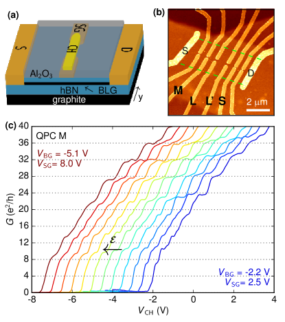
The device geometry is similar to the one employed in our demonstration of full pinch-off of bilayer graphene quantum point contacts Overweg et al. (2018). A bilayer graphene (BLG) flake was encapsulated between hexagonal boron nitride layers (hBN), using the van der Waals pick-up technique Wang et al. (2013), and deposited onto a graphite flake (see Figure 1a for a schematic of the final device geometry). The graphene layer was contacted with Cr/Au contacts and a top gate pattern, consisting of six pairs of split gates (SG) with spacings ranging from 50 nm to 180 nm, was evaporated. On top of the device a layer of Al2O3 and finally the channel gates (CH) were deposited. An atomic force microscopy image of the sample, recorded prior to the deposition of the channel gates, is shown in Fig. 1b. In the present manuscript, we show data from three QPCs: QPC S (50 nm split gate separation), QPC M (80 nm) and QPC L (180 nm).
By applying voltages of opposite sign to the graphite back gate and the split gates, a band gap is induced McCann and Fal’ko (2006) in the bilayer graphene. In Ref. 15 we demonstrated that this suppresses transport below the split gates. Hence a constriction is formed, in which the charge carrier density can be tuned by the channel gate voltage. During the measurements only a single pair of split gates was biased at a time to form a QPC. The measurements were performed at K.
The conductance of QPC M (80 nm wide) as a function of channel gate voltage is shown in Fig. 1c for various combinations of the split and back gate voltage. For each curve, a series resistance was subtracted which corresponds to the resistance measured at the same back gate voltage with uniform charge carrier density throughout the sample. The traces show several plateaus with a typical step size of , in particular for large quantum numbers, as previously reported in Ref. 15. Similar results have been found for QPC L and L’ (180 nm wide) with a smaller spacing in gate voltage between the plateaus, in agreement with the wider channel, and for QPC S (50 nm wide) with a larger spacing. For the employed range of gate voltages, the displacement field does not significantly change the observed plateau sequence. Below we observe several kinks which cannot be identified as plateaus and some plateaus occurring below the expected conductance values. Reduced screening of the disorder potential in this low density regime might play a role. Simulations of the electrostatic potential Overweg et al. (2018) show that in this regime the confinement potential is shallow. From a theoretical perspective the non-monotonicity of the dispersion relation, which becomes more pronounced for larger gaps and wider channels, can lead to additional degeneracies for low mode numbers, possibly explaining the absence of a plateau at Knothe and Fal’ko (2018).
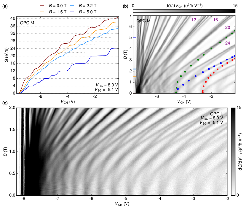
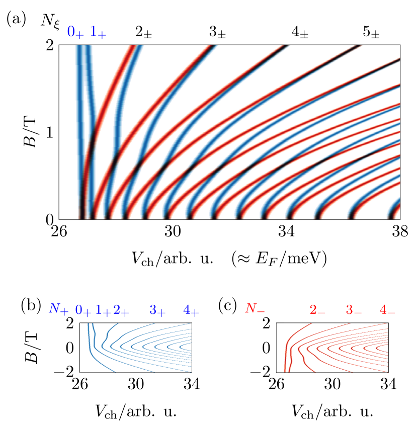
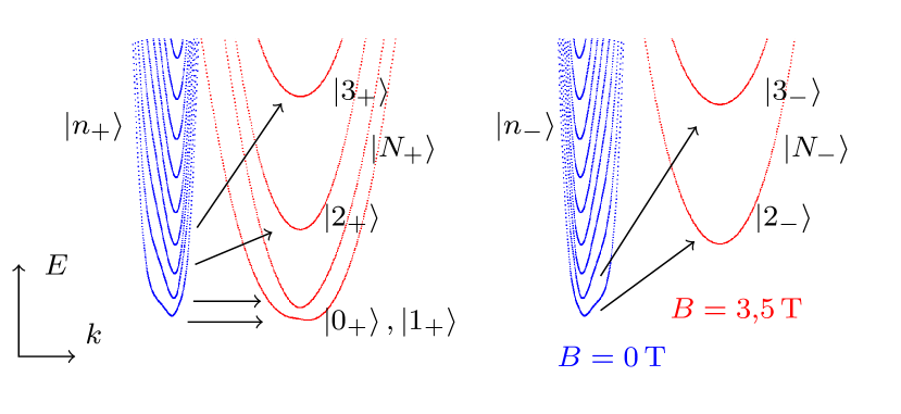
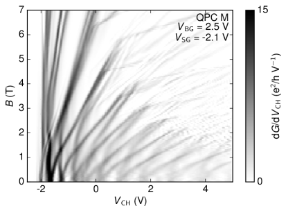
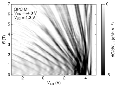
The conductance of QPC M as a function of channel gate voltage for several magnetic field strengths (Figure 2a) features a plateau sequence at described by with integer . Increasing the magnetic field to a value of T changes the plateau sequence to . At T the conventional sequence of Landau levels of BLG is observed, with . In the lowest two Landau levels a lifting of the fourfold degeneracy can be observed. Around T, during the transition to the Hall regime, the fourfold degeneracy is restored: the sequence is shifted to . This is most clearly visible for the modes for which .
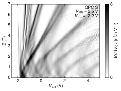
To further investigate this transition we inspect the transconductance as a function of channel gate voltage and magnetic field (see Fig. 2b). Mode transitions show up as dark lines, which start out vertically in low magnetic fields, but bend toward more positive gate voltages above T. This phenomenon, known as magnetic depopulation and observed for instance in high quality GaAs, is due to the transition from electrostatic confinement to magnetic confinement. What is unusual however, is the pattern of mode splittings and mode crossings.
The same pattern can be observed for the wider QPCs (Fig. 2c), where the fourfold degeneracy is already restored at 2 T because of the wider channel. Although the lowest modes are hard to resolve, a robust pattern of mode crossings can be observed for many higher modes. Similar patterns could be observed for various displacement fields inside the channel and also for a -doped channel (see Appendices I and J).
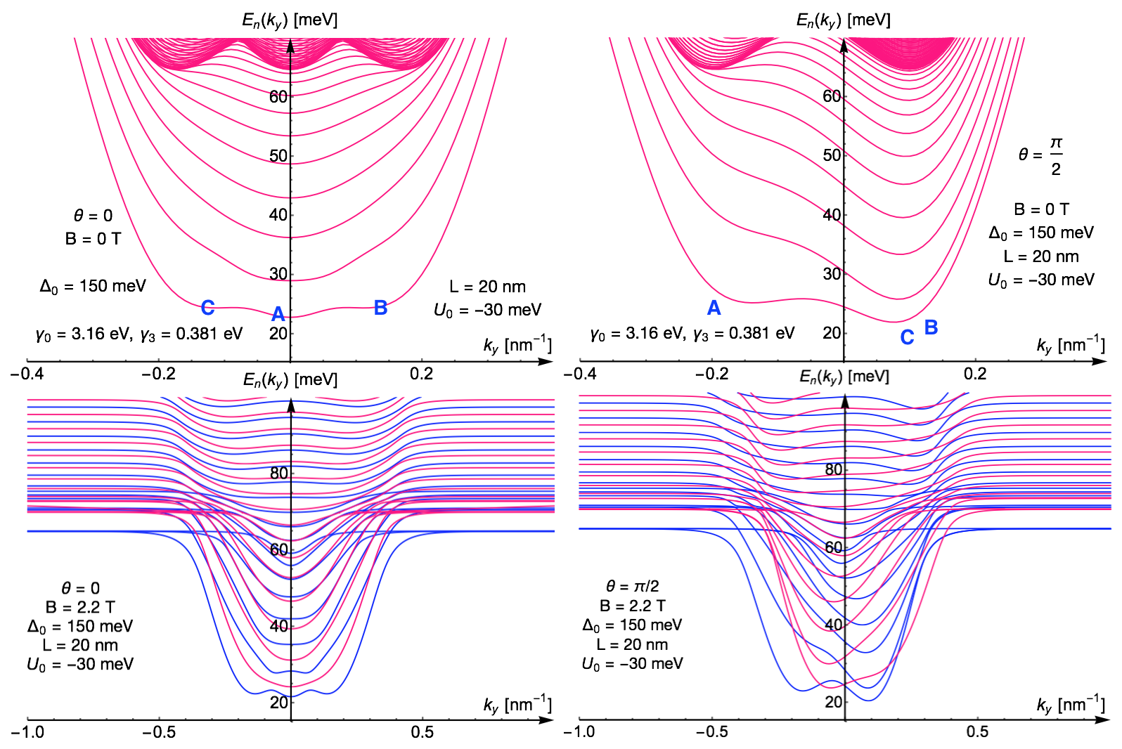
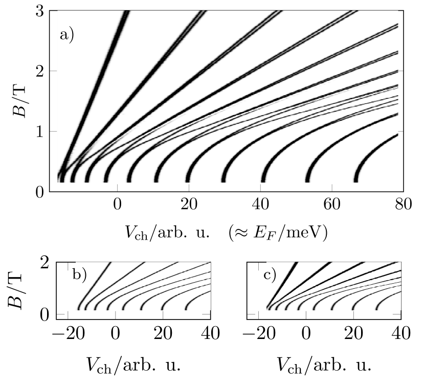
To elucidate the evolution of the conductance steps with magnetic field, we simulate the experimental setup using two independent, complementary theoretical approaches, theory McCann and Fal’ko (2006) and tight-binding calculations Libisch et al. (2012) (see the supplement for technical details). Both approaches agree well with each other and the experiment, highlighting the robustness of the observed features and the validity of our two modelling approaches. They reproduce and explain the observed low-field splitting (Fig. 3) and the level crossing pattern (Fig. 4).
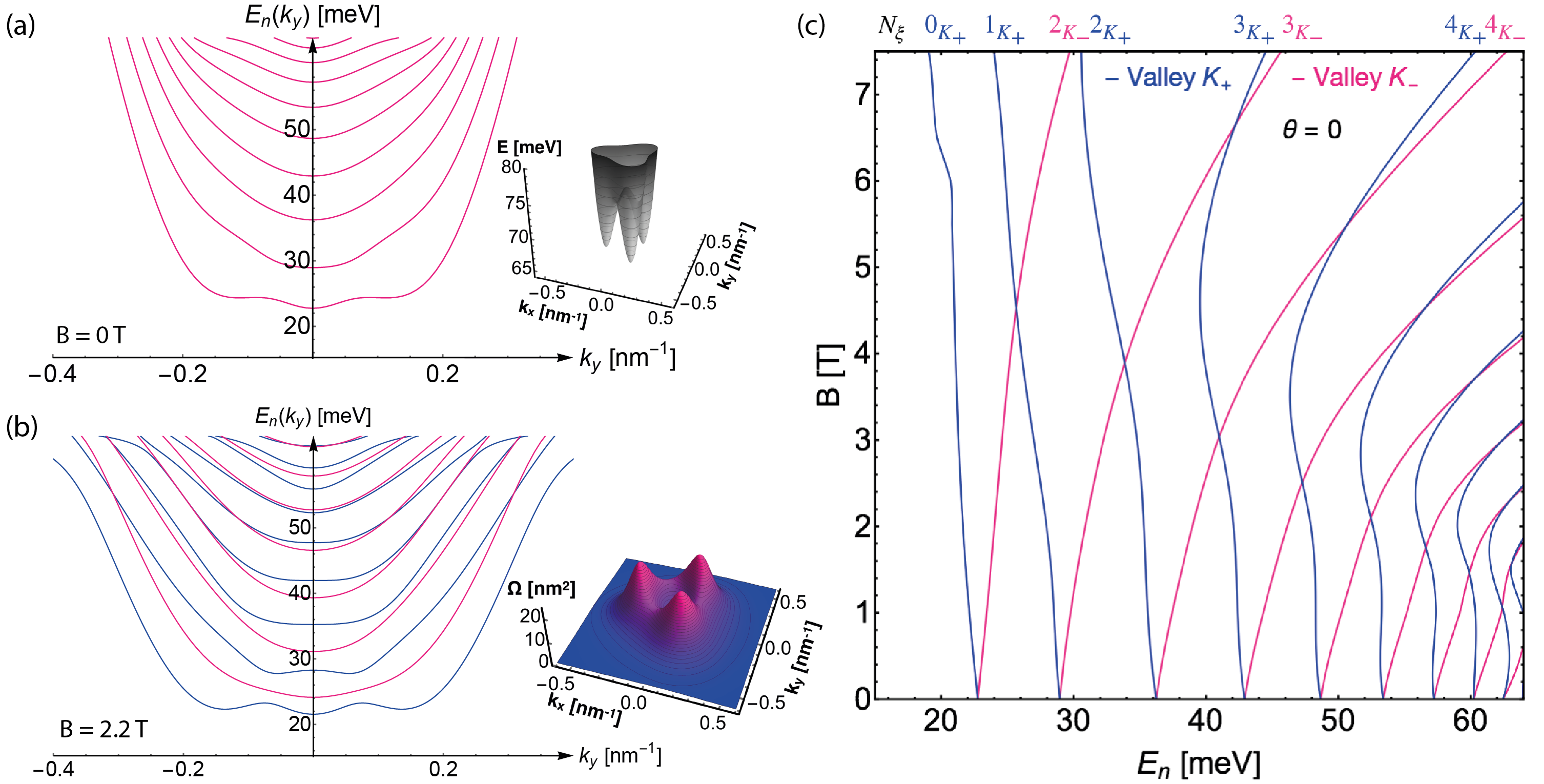
Here, we use soft electrostatic confinement provided by a transverse electric field both at and at a finite magnetic field. The obtained magnetic field dependence of the miniband edges represents the closest spectral analogue of the experimentally measured transconductance spectrum. We chose the potential landscape for theory by matching the mode spacing extracted from finite bias measurements of QPC M at T (see Appendix K). Note that in the experiment the channel gate voltage influences not only the Fermi level, but also the shape of the confinement potential and the size of the displacement field inside the channel. To obtain one to one agreement between the calculation and the experimental results, a self-consistent potential would be required.
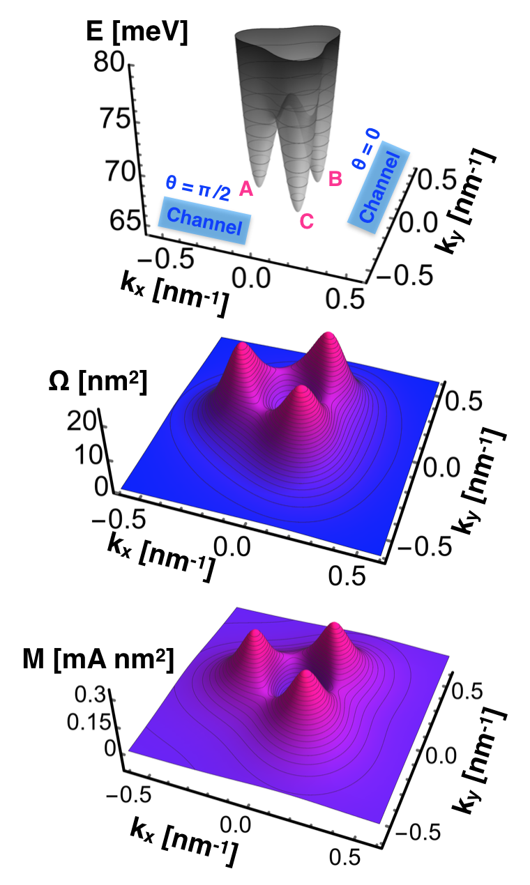
At zero magnetic field, we find spin- and valley-degenerate spectra (Fig. 3a) in agreement with the experimentally observed step size of (Fig. 2a). The subband edges (for small mode numbers) are situated at finite momenta, reminiscent of the three mini-valleys in gapped BLG in the presence of trigonal warping McCann and Fal’ko (2006); Varlet et al. (2014). When switching on a magnetic field, the interlayer asymmetry leads to valley splitting of electron subbands, clearly seen in the band structure computed for T (Fig. 3b, blue and magenta subbands). This lifting of valley degeneracy is in agreement with the measured step size of (see Fig. 2a). The linearity of the valley splitting of the subband edges with , Fig. 3b, is related to the fact that the zero-field states (with transverse quantum number in the () valley) of trigonally warped gapped BLG McCann and Fal’ko (2006); Varlet et al. (2014) carry non-trivial Berry curvature (see insets of Fig. 3 and in Appendix B) and, consequently, a finite magnetic moment, . For larger displacement fields, the Berry curvature becomes more spread out in -space around the K-points, affecting several of the lowest modes.
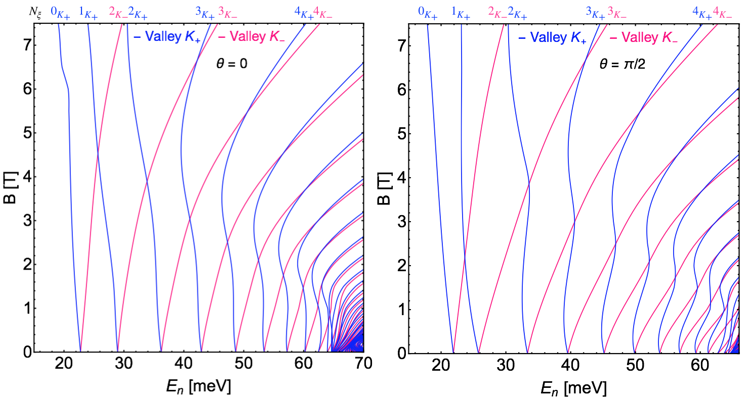
In the high magnetic field regime, where the magnetic length is smaller than the channel width, the subbands in the channel become drifting states in the BLG Landau levels (LLs) , where now indicates the LL index. The LL spectrum of BLG has a pair of special states , that appear at zero energy in ungapped BLG with the wave functions residing on different layers in the opposite valleys. After the displacement field introduces a layer asymmetry gap, these states split apart by , resulting in the two lowest conduction band subbands belonging to only one valley, e.g. (then, the highest valence band subbands would be from valley ). The other LLs in both valleys with have approximately the same weight on the sublattices in the two layers and very close energies. Such an asymptotic behavior corresponds to the evolution of the subbands such that subbands eventually merge with subbands upon an increase in magnetic field as shown in Fig.4a. For , the same pattern emerges with the two valleys interchanged (see Fig. 4b,c).
Note that the absence of hard edges characteristic for the present electrostatically defined bilayer constriction is critical for observing the interweaving pattern of crossing states. In rough-edged constrictions broken valley symmetry due to scattering quickly obscure the underlying pattern. These difficulties aside, a similar crossing pattern appears in principle in single layer graphene, as we have verified numerically for an ideal constriction (see Appendix G).
In conclusion, we reported on the experimental observation of the mode crossing pattern during the evolution from size quantization to the Hall regime in BLG QPC. A valley splitting linear in magnetic field could be explained by a non-trivial orbital magnetic moment of states in gapped BLG. Our experimental results could be reproduced by numerical simulations.
Acknowledgements
We thank A. Rebhan for fruitful discussions. We acknowledge financial support from the European Graphene Flagship, the Swiss National Science Foundation via NCCR Quantum Science and Technology, ERC Synergy Hetero 2D, WWTF project MA14-002 and MECD. Calculations were performed on the Vienna Scientific Cluster (VSC). Growth of hexagonal boron nitride crystals was supported by the Elemental Strategy Initiative conducted by MEXT, Japan and the CREST (JPMJCR15F3), JST.
References
- Wees and Houten (1988) BJ Van Wees and H Van Houten, “Quantized conductance of point contacts in a two-dimensional electron gas,” Physical Review Letters 60, 848–850 (1988).
- Wharam et al. (1988) D A Wharam, T J Thornton, R Newbury, M Pepper, H Ahmed, J E F Frost, D G Hasko, D C Peacock, D A Ritchie, and G A C Jones, “One-dimensional transport and the quantisation of the ballistic resistance,” Journal of Physics C: Solid State Physics 21, L209–L214 (1988).
- Rokhinson et al. (2006) L. P. Rokhinson, L. N. Pfeiffer, and K. W. West, “Spontaneous spin polarization in quantum point contacts,” Physical Review Letters 96, 156602 (2006).
- Danneau et al. (2006) R. Danneau, W. R. Clarke, O. Klochan, A. P. Micolich, A. R. Hamilton, M. Y. Simmons, M. Pepper, and D. A. Ritchie, “Conductance quantization and the 0.7x2e2/h conductance anomaly in one-dimensional hole systems,” Applied Physics Letters 88 (2006), 10.1063/1.2161814.
- Többen et al. (1995) D Többen, D A Wharam, G Abstreiter, J P Kotthaus, and F Schäffler, “Ballistic electron transport through a quantum point contact defined in a {Si/Si_{0.7}Ge_{0.3}} heterostructure,” Semicond. Sci. Technol. 10, 711–714 (1995).
- Chou et al. (2005) H. T. Chou, S. Lüscher, D. Goldhaber-Gordon, M. J. Manfra, A. M. Sergent, K. W. West, and R. J. Molnar, “High-quality quantum point contacts in GaNAlGaN heterostructures,” Applied Physics Letters 86, 1–3 (2005).
- Goel et al. (2005) N. Goel, J. Graham, J. C. Keay, K. Suzuki, S. Miyashita, M. B. Santos, and Y. Hirayama, “Ballistic transport in InSb mesoscopic structures,” Physica E: Low-Dimensional Systems and Nanostructures 26, 455–459 (2005).
- Gunawan et al. (2006) O. Gunawan, B. Habib, E. P. De Poortere, and M. Shayegan, “Quantized conductance in an AlAs two-dimensional electron system quantum point contact,” Physical Review B 74, 155436 (2006).
- Mizokuchi et al. (2018) R. Mizokuchi, R. Maurand, F. Vigneau, M. Myronov, and S. De Franceschi, “Ballistic one-dimensional holes with strong g-factor anisotropy in germanium,” , 1–23 (2018).
- Tombros et al. (2011) Nikolaos Tombros, Alina Veligura, Juliane Junesch, Marcos H. D. Guimarães, Ivan J. Vera Marun, Harry T. Jonkman, and Bart J. van Wees, “Quantized conductance of a suspended graphene nanoconstriction,” Nature Physics 7, 697–700 (2011).
- Terrés et al. (2016) B. Terrés, L. A. Chizhova, F. Libisch, J. Peiro, D. Jörger, S. Engels, A. Girschik, K. Watanabe, T. Taniguchi, S. V. Rotkin, J. Burgdörfer, and C. Stampfer, “Size quantization of Dirac fermions in graphene constrictions,” Nature Communications 7, 1–7 (2016).
- Kim et al. (2016) Minsoo Kim, Ji-Hae Choi, Sang-Hoon Lee, Kenji Watanabe, Takashi Taniguchi, Seung-Hoon Jhi, and Hu-Jong Lee, “Valley-symmetry-preserved transport in ballistic graphene with gate-defined carrier guiding,” Nature Physics (2016), 10.1038/nphys3804.
- Allen et al. (2012) M T Allen, J Martin, and A Yacoby, “Gate-defined quantum confinement in suspended bilayer graphene.” Nature Communications 3, 934 (2012).
- Goossens et al. (2012) Augustinus Stijn M Goossens, Stefanie C M Driessen, Tim A Baart, Kenji Watanabe, Takashi Taniguchi, and Lieven M K Vandersypen, “Gate-defined confinement in bilayer graphene-hexagonal boron nitride hybrid devices.” Nano Letters 12, 4656–60 (2012).
- Overweg et al. (2018) Hiske Overweg, Hannah Eggimann, Xi Chen, Sergey Slizovskiy, Marius Eich, Pauline Simonet, Riccardo Pisoni, Yongjin Lee, Kenji Watanabe, Takashi Taniguchi, Vladimir Fal’ko, Klaus Ensslin, and Thomas Ihn, “Electrostatically induced quantum point contact in bilayer graphene,” Nano Letters 18, 553–559 (2018).
- Redlich (1984) A. N. Redlich, “Parity violation and gauge noninvariance of the effective gauge field action in three dimensions,” Physical Review D 29, 2366–2374 (1984).
- Sui et al. (2015) Mengqiao Sui, Guorui Chen, Liguo Ma, Wen Yu Shan, Dai Tian, Kenji Watanabe, Takashi Taniguchi, Xiaofeng Jin, Wang Yao, Di Xiao, and Yuanbo Zhang, “Gate-tunable topological valley transport in bilayer graphene,” Nature Physics 11, 1027–1031 (2015), arXiv:1501.04685 .
- Cortijo et al. (2012) A. Cortijo, F. Guinea, and M. A.H. Vozmediano, “Geometrical and topological aspects of graphene and related materials,” Journal of Physics A: Mathematical and Theoretical 45 (2012), 10.1088/1751-8113/45/38/383001, arXiv:1112.2054 .
- Novoselov et al. (2006) K. S. Novoselov, E. McCann, S. V. Morozov, V. I. Fal’ko, M. I. Katsnelson, U. Zeitler, D. Jiang, F. Schedin, and A. K. Geim, “Unconventional quantum Hall effect and Berry’s phase of 2 in bilayer graphene,” Nature Physics 2, 177–180 (2006), arXiv:0602565 [cond-mat] .
- Rao and Sood (2013) C.N.R. Rao and A.K. Sood, Graphene: Synthesis, Properties, and Phenomena (Wiley, 2013).
- Taychatanapat et al. (2011) T. Taychatanapat, K. Watanabe, T. Taniguchi, and P. Jarillo-Herrero, “Quantum hall effect and landau-level crossing of dirac fermions in trilayer graphene,” Nature Physics 7, 621–625 (2011).
- Wang et al. (2013) L Wang, I Meric, P Y Huang, Q Gao, Y Gao, H Tran, T Taniguchi, K Watanabe, L M Campos, D a Muller, J Guo, P Kim, J Hone, K L Shepard, and C R Dean, “One-dimensional electrical contact to a two-dimensional material.” Science 342, 614–7 (2013).
- McCann and Fal’ko (2006) Edward McCann and Vladimir I. Fal’ko, “Landau-level degeneracy and quantum hall effect in a graphite bilayer,” Physical Review Letters 96, 086805 (2006), arXiv:0510237 [cond-mat] .
- Knothe and Fal’ko (2018) A. Knothe and V. Fal’ko, “How do minivalleys and berry curvature influence electrostatically induced conduction channels in gapped bilayer graphene?” (2018).
- Libisch et al. (2012) F. Libisch, S. Rotter, and J. Burgdörfer, “Coherent transport through graphene nanoribbons in the presence of edge disorder,” New Journal of Physics 14, 123006 (2012).
- Varlet et al. (2014) Anastasia Varlet, Dominik Bischoff, Pauline Simonet, Kenji Watanabe, Takashi Taniguchi, Thomas Ihn, Klaus Ensslin, Marcin Mucha-Kruczyński, and Vladimir I. Fal’ko, “Anomalous Sequence of Quantum Hall Liquids Revealing a Tunable Lifshitz Transition in Bilayer Graphene,” Physical Review Letters 113, 116602 (2014).
- Xiao et al. (2010) Di Xiao, Ming Che Chang, and Qian Niu, “Berry phase effects on electronic properties,” Reviews of Modern Physics 82, 1959–2007 (2010), arXiv:0907.2021 .
- Chang and Niu (1995) Ming Che Chang and Qian Niu, “Berry phase, hyperorbits, and the Hofstadter spectrum,” Physical Review Letters 75, 1348–1351 (1995), arXiv:9511014 [cond-mat] .
- Jung and MacDonald (2014) Jeil Jung and Allan H. MacDonald, “Accurate tight-binding models for the bands of bilayer graphene,” Physical Review B - Condensed Matter and Materials Physics 89, 035405 (2014).
- Sanvito et al. (1999) S. Sanvito, C.J. Lambert, J.H. Jefferson, and A.M. Bratkovsky, “General green’s-function formalism for transport calculations with spd hamiltonians and giant magnetoresistance in co- and ni-based magnetic multilayers,” Phys. Rev. B 59, 11936–11948 (1999).
Appendix A Model Hamiltonian
The four-band model Hamiltonian of BLG (BLG) is given by McCann and Fal’ko (2006); Varlet et al. (2014)
| (1) |
written in the basis or in the two valleys (for ), and (for ). The diagonal terms in this Hamiltonian account for the spatially modulated confinement potential and the modulated gap :
| (2) |
where we chose meV, nm, and , in accordance with the parameters of the experimental probes. Furthermore, , , with and for the velocities and hoppings we use m/s, m/s, and meV Varlet et al. (2014).
Appendix B Bulk properties
In the limit the Hamiltonian of Eg. 1 describes the properties of homogeneous gapped BLG. The dispersion is given by the four valley degenerate bands McCann and Fal’ko (2006)
| (3) |
where , and . In the top panel of Fig. 5 we plot the lower conduction band () in the valley for a gap of meV demonstrating the effect of trigonal warping induced by causing the dispersion to form three mini-valleys around each -point. The states of gapped BLG carry a non-trivial Berry curvature and orbital magnetic moment. From the Bloch functions of the th band the magnitude of the corresponding Berry curvature and the orbital magnetic moment can be computed according to Refs. Xiao et al. (2010); Chang and Niu (1995)
where and denotes the two-dimensional cross product. We plot the Berry curvature and the magnetic moment of the lower conduction band in the -valley in the lower panels of Fig. 5 for meV. In the -valley both and carry the opposite sign. A non-zero orbital magnetic momentum behaves like the electron spin Xiao et al. (2010) and will hence couple linearly to a magnetic field through a Zeeman-like term .
Appendix C Numerical diagonalization inside the channel
In the presence of a nontrivial confinement potential we diagonalize the Hamiltonian in Eq. 1 numerically in a basis of harmonic oscillator wave functions , where is the normalization constant and is a scaling factor of unit length-1; we choose adapted to the potential obtained from comparing a parabolic potential to . We assume free propagation of the electrons in the -direction. The basis states are then of the form where the -dependent part is given by
| (4) |
For every set of system parameters we construct the matrix corresponding to Hamiltonian in the basis given in Eq. 4 and obtain the energy spectrum by diagonalization. Convergence is reached when the energy levels do not change anymore upon including a higher number of basis states. In order to include a magnetic field we do Peierls substitution in the Hamiltonian in Eq. 1 : . For a magnetic field perpendicular to the BLG sheet and to preserve translational invariance in the -direction we chose Landau gauge of the form The basis states of Eq. 4 then translate into the basis of Landau level wave functions localized at Landau orbital .
Appendix D Channel spectra for different parameters
Due to the trigonal warping effect for non-zero the dispersion is not rotationally symmetric (c.f. the dispersion of homogeneous gapped BLG in Fig. 5) and the channel spectra therefore depend on the orientation of the channel. We distinguish between the two angles of orientation and for which the orientation of the channel is indicated by the blue bars in Fig. 5. In Fig. 6 we show additional channel spectra for different system parameters and the two different angles of orientation. Figure 7 shows the dependence of the lower band edges as a function of the magnetic field for both angles. \onecolumngrid@push
Appendix E Details of the tight binding simulation
Our tight binding calculation is done for a 280 nm wide BLG nanoribbon in the parametrisation given by Jung et al. Jung and MacDonald (2014). An additional displacement field, which we obtain from solving the Poisson equation for the experimental setup QPC L at constant channel voltage V, is added. It confines the wavefunctions to the 180 nm wide region between the gates, where the displacement field is about 50 meV. A Berry-Mondragon type potential at the sides of the ribbon is used to eliminate edge states, restricting the simulation effectively to a width of 250 nm. We then solve the eigenvalue problem for the Bloch state Sanvito et al. (1999)
| (5) |
for a given numerically, which has wavefunctions of an infinite waveguide as solutions. The bandstructure is given by the eigenvalues , see Fig. 8. The matrix contains all on-site energies and hopping matrix elements of a slice in direction, and the matrix contains the hopping matrix elements between a given slice and the one to the right, separated by . As direction of propagation we choose an angle rad away from armchair direction. In armchair direction, the two cones lie on top of each other in momentum space, making a clean separation of and states challenging.
Appendix F Effective low-energy Hamiltonian
The minimal ingredients which lead to the observed crossing pattern are already present in the effective low-energy Hamiltonian of BLG. For completeness, we present a short discussion.
We consider Bernal-stacked BLG, with and atoms in the lower layer, and (coupled to ) and atoms in the upper layer. Eliminating the dimer state components leads to an effective low-energy Hamiltonian written in terms of the wavefunction on the unpaired ( and ) atoms, A magnetic field , , can be added with the minimal coupling prescription . With the confinement in direction in mind, we choose the gauge . The Hamiltonian then reads
| (6) |
where we define the magnetic length and , , interlayer coupling , Fermi velocity , valley index . It has the solutions McCann and Fal’ko (2006) for and
| (7) |
and two zero-energy solutions
| (8) |
The localization of the lowest lying Landau on a single sublattice results – due to the absence of nearest neighbors – in zero-energy solutions of the effective Hamiltonian. Near we find the same spectrum but with the and sublattices reversed.
Magnetic Field and displacement field
A displacement field acts as an effective mass term and lifts the degeneracyMcCann and Fal’ko (2006),
| (9) |
The two zero modes are shifted above () or below () the gapMcCann and Fal’ko (2006),
| (10) |
The states which are localized on one sublattice and thus localized on one of the layers are trivially affected by the electrostatic potential: The zeroth Landau levels where is positive gets shifted above the gap, and the level where is negative is shifted below the gap.
Appendix G Monolayer Graphene
A similar effect can be observed in monolayer graphene, see Fig. 9.
The only difference is that due to the existence of a single zero mode instead of two in the quantum Hall regime, the evolution now follows the pattern and for positive , and with the roles of and reversed for negative .
Appendix H Transconductance of QPC S
The transconductance of QPC S as a function of channel gate voltage and magnetic field is shown in Fig. 10. It shows a pattern of mode crossings similar to the patterns of QPC M and QPC L (see Fig. 2b,c), with a larger mode spacing due to the narrower confinement potential.
Appendix I Transconductance in a lower displacement field
Figure 11 shows the transconductance of QPC M as a function of channel gate voltage and magnetic field for and . Although this corresponds to a smaller displacement field in the channel than in Fig. 2b, a similar pattern of mode crossings is observed. No modes can be observed in the top right corner of Fig. 11, because in this regime the filling factor in the bulk is smaller than the filling factor in the channel.
Appendix J Transconductance in the -type regime
The pattern of mode crossing can also be observed for a -type channel, as shown for QPC M in Fig. 12.
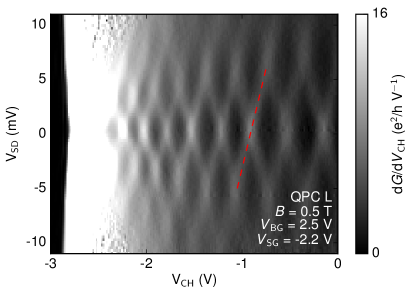
Appendix K Finite bias diamonds
Figure 13 shows the finite bias measurements of the modes of QPC L, showing a mode spacing on the order of 3 meV at T. From the slope of the diamond boundaries (see red dashed line in Fig. 13), a lever arm for conversion from channel gate voltage to energy can be extracted (). For QPC L we find and for QPC M we find . The smaller lever arm for the narrower QPC is due to more significant screening of the channel gate voltage for this QPC.