Narrow photoluminescence peak of epitaxial MoS2 on graphene/Ir(111)
Abstract
We report on the observation of photoluminescence (PL) with a narrow 18 meV peak width from molecular beam epitaxy grown on graphene/Ir(111). This observation is explained in terms of a weak graphene-MoS2 interaction that prevents PL quenching expected for a metallic substrate. The weak interaction of MoS2 with the graphene is highlighted by angle-resolved photoemission spectroscopy and temperature dependent Raman spectroscopy. These methods reveal that there is no hybridization between electronic states of graphene and MoS2 and a different thermal expansion of graphene and MoS2. Molecular beam epitaxy grown MoS2 on graphene is therefore an important platform for optoelectronics which allows for large area growth with controlled properties.
1 Introduction
Following in the wake of graphene research, the optical properties of monolayer and related materials have stimulated intense research efforts over the last years [1, 2, 3]. The MoS2 monolayer can take the form of 2H or 1T (1T’) crystal structures [4], with the 2H phase being a two-dimensional semiconductor with a direct band gap that exhibits photoluminescence [1]. Research has shown promise for applications of as field effect transistors, electroluminescent devices [5, 6] and in the area of spintronics [7]. However, most progress in our understanding of this material is still based on exfoliated layers, e.g. the recently observed record narrow luminescence of 5 meV [8]. Small flake size and the inherent inability of exfoliation for scale up impedes not only scientific research using methods where a large area film with a single orientation is needed. It also precludes the development of based electronics. A clean and scalable approach to MoS2 and other transition metal dichalcogenide synthesis is very low pressure chemical vapour deposition (CVD) using a catalytically active metallic substrate to support the decomposition of a sulphur containing precursor molecule. For example, simultaneous supply of Mo and H2S molecules yields large islands and even single domain monolayer coverage of MoS2 on Au(111) [9, 10]. However, the substantial interaction and hybridization of the layer with the metallic substrate modifies the properties of the layer substantially. This is a drawback specifically when considering potential applications in optics. Due to the low reactivity of van der Waals substrates like graphene or hexagonal boron nitride, neither phase pure layers nor a well defined epitaxial relation could be realized up to now with such sulphur containing precursor molecules [11]. Through molecular beam epitaxy (MBE) using elemental sulphur – supplied e.g. from a valved sulphur cracker cell or from a Knudsen cell releasing elemental sulphur out of a compound like FeS2 – phase pure and epitaxial transition metal disulfide layers could be grown even on van der Waals substrates to which they are only weakly bonded [12, 13].
However, a complete spectroscopic characterization of such heterostructures is missing so far despite the fundamental interest in MoS2 on graphene () e.g. as a photodetector [14]. Moreover, none of the above mentioned works on MBE grown reported optical (photoluminescence or Raman) characterization of the material. This is surprising because optical methods are a main tool for the investigation of exfoliated [3]. The lack of optical spectroscopy characterization for MBE grown MoS2 might be explained by the fact that these methods are less prevalent in the MBE community.
The present manuscript addresses these points and, besides structural investigation, investigates MBE-grown spectroscopically using X-ray photoemission spectroscopy (XPS), angle-resolved photoemission spectroscopy (ARPES) and optical (Raman and luminescence) methods. For the monolayer islands of epitaxially grown on a closed layer of graphene on Ir(111), as seen by scanning tunneling microscopy (STM) and low energy electron diffraction (LEED), the band structure measured by ARPES highlights the absence of any hybridization between and graphene. Our results reveal that the photoluminescence (PL) of /Gr/Ir(111) is present despite the metallic substrate. We compare the optical bandgap obtained from PL measurements of the pristine /Gr/Ir(111) system to the energy separation between valence and conduction bands of the lithium (Li) doped system that we measured using ARPES. By careful analysis of this data and taking into account the doping induced bandgap renormalization, we estimate an exciton binding energy of 480meV. The temperature dependence of the bond lengths in graphene and is probed using Raman spectroscopy. We find that the lattice expansion of graphene and behave completely different. Graphene’s lattice expansion is dictated by the underlying Ir. The layer of , which is not in direct contact to the Ir(111), roughly follows the lattice expansion expected for freestanding MoS2. Our findings introduce MBE grown /Gr as a highly ordered, epitaxial heterostructure with a sharp optical emission that can be grown in large scale.
2 Experimental Results
2.1 Structure and electronic properties
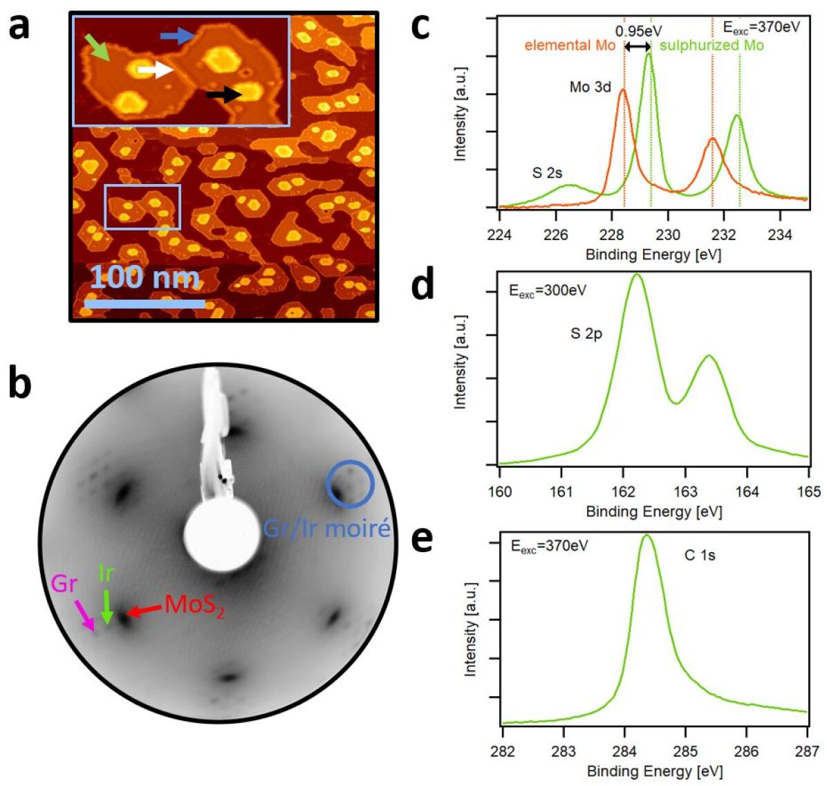
Prior to the analysis of the electronic and optical properties of the MoS2 layer, we present in Figure 1 its microscopic, structural and chemical characterization. In (a), a large scale STM topograph of the MoS2 island layer is shown. The islands rest on the Gr/Ir(111) substrate, which has two monatomic step edges crossing the topograph horizontally. A large fraction of the substrate is covered by monolayer islands (green arrow in the inset), decorated with small bilayer islands (black arrow). On both, the monolayer and the bilayer, a metallic edge state surrounding the islands can be observed (blue arrow), since the bias voltage lies in the band gap of the semiconductor MoS2. Bright lines, running across the MoS2 islands can be identified as (mirror) twin boundaries (white arrow) [15]. The MoS2 islands are extremely clean with a negligible density of defects. Subfigure (b) displays a LEED pattern of the sample, indicating the epitaxial relation between the substrate and the adlayer. Going from outside to inside, the first order Gr and Ir(111) spots and their associated moiré can be seen. Farthest inside, slightly rotationally broadened first order MoS2 diffraction spots indicate a lattice constant of , in line with the literature [16]. To probe the chemical properties, XPS was performed. Figure 1(c) compares the Mo 3d core level of elemental molybdenum in red (produced by evaporating molybdenum onto the Gr/Ir(111) surface without any source for sulfur) to the grown MoS2/Gr/Ir(111) structure in green. It can be seen that the Mo 3d core level is shifted to higher binding energy by 0.95 eV. This shift is in line with earlier observations of MoS2 grown on a gold substrate [17]. In these previous results, a splitting of the Mo 3d core level was observed into three components (low binding-energy, mid binding-energy and high binding-energy component) [17]. In comparison, our Mo 3d peak lacks the reported low binding-energy and mid binding-energy components which are attributed to metallic Mo and Mo on the edge of a flake. For the low binding-energy peak, we attribute this to the fact that all available Mo was used up in the reaction to form MoS2 and no elemental Mo is left over. The absence of the mid binding-energy component can be explained by the large island size achieved in this work. This increases the “bulk” versus the edge contribution to a point where the edge contribution is negligible. The sulfur 2p peak is shown in Figure 1(d). Our analysis confirms the growth of crystalline MoS2 and the absence of amorphous MoS3 [18]. Results of MoS2 grown on gold show an asymmetry in the S 2p peak [10] compared to the present work. This can be explained by the influence of the gold substrate on the lower sulfur layer. This asymmetry is not visible for MoS2/Gr/Ir(111), suggesting a negligible influence of the Gr/Ir(111) substrate on the lower sulfide layer and thus a weak interaction of the substrate with the grown MoS2 islands. As we will discuss later, this weak interaction is key to observing PL. The C 1s peak of the graphene layer is shown in Figure 1(e).
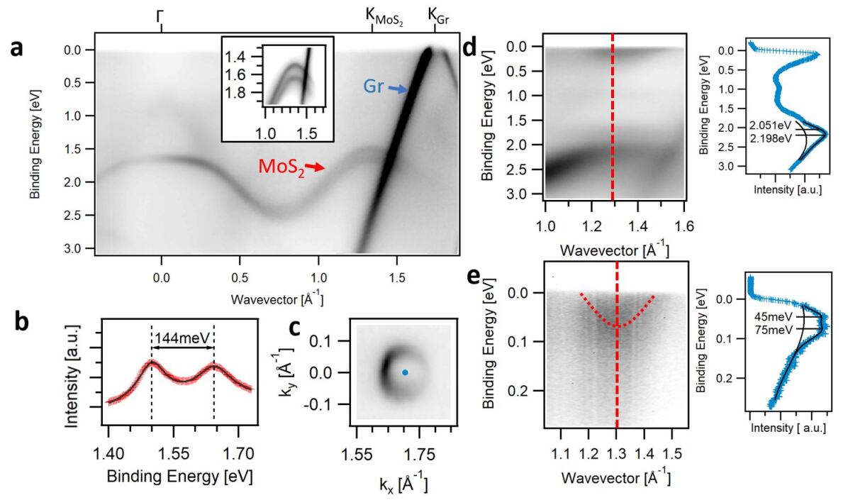
Figure 2 shows angle-resolved photoemission spectroscopy (ARPES) results of the same system. An overview scan depicting the bands of graphene, and the Ir substrate is shown in Figure 2(a). The point of graphene is at 1.7 and the point of at 1.3 , both are indicated at the top x-axis. The valence band (VB) maximum of appears at the -point consistent with monolayer MoS2. For comparison, bilayer MoS2 (shown in the supporting information) has the VB maximum at the point. By taking the distance between the VB maximum of at the -point to the Fermi level (approximately 1.5 eV), it suggests that the Fermi level is closer to the conduction band (CB) than to the valence band of as the measured electronic bandgap is typically below 2.6 eV[3]. The splitting of the VB at due to spin-orbit interaction is clearly seen in the high resolution scan shown in the inset to Figure 2(a). The fit to the energy distribution curve from a cut through the MoS2 -point is shown in Figure 2(b) and reveals a spin-orbit coupling of 144 meV. Interestingly, graphene is more hole doped than it was before growth, the Dirac-point binding energy is evaluated to be compared to in the pristine case [19]. The hole doping can be seen from the ARPES scans and the map shown in Figures 2(a,c). The fact that hole doping increases after performing the MoS2 growth on Gr/Ir(111) is also evident from a comparison to other works on Gr/Ir(111) [20, 21]. Analysis of the Fermi surface yields a hole concentration of . As we will see later, this hole doping is also responsible for the shift of the Raman active band of Gr. Notably, ARPES does not show any hybridization between MoS2 and graphene bands which supports the idea that MoS2 is weakly interacting with Gr.
In order to measure the CB edge using ARPES, we have performed Li doping which induces an electron transfer from Li to the MoS2 layer thereby populating its CB. Figures 2(d,e) show ARPES spectra of Li doped MoS2/Gr heterostructures. The doping turns MoS2 into a metal which is corroborated from the ARPES observation of a CB at the point of MoS2 (the CB is visible as a parabola at the Fermi level in Figure 2(e)). Assuming a circular Fermi surface of Li-doped MoS2, we estimate an electron concentration of per cm2.
The VB shifts down in energy and broadens but is otherwise unchanged. A Li induced phase transition in MoS2 has been predicted theoretically [22, 23] and experimentally reported in Li intercalated quantum dots [24]. Interestingly, in the present system we do not observe a structural phase transition of MoS2 to a 1T (or 1T’) phase which would be visible as a different band structure in the ARPES measurements [25, 23]. An energy distribution curve (EDC) through the point yields peaks at 75 meV (CB minimum) and 2.05 eV (upper VB maximum). Their difference is equal to 1.975 eV. This value is similar to what has been measured in potassium intercalated monolayer MoS2 on bulk MoS2 where 1.86 eV was found [26]. In the next section we compare the obtained VB-CB separation to the energy of the PL to estimate a lower bound of the exciton binding energy.
.
2.2 Luminescent properties
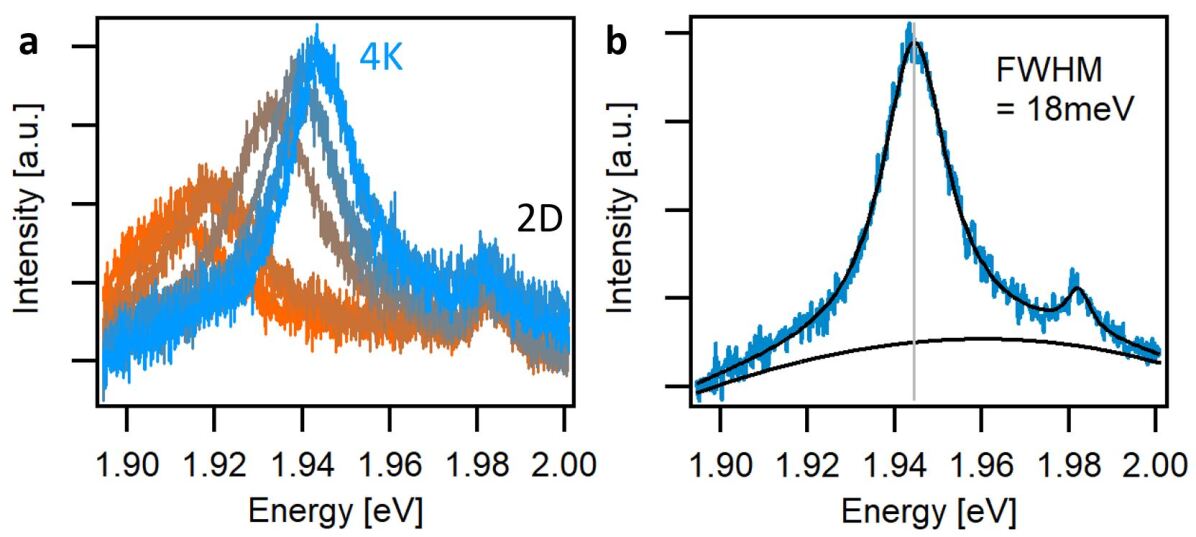
Samples prepared and characterized in this way have then been transferred without exposure to air to an ultra-high-vacuum (UHV) PL/Raman system [27]. Despite the MoS2 islands are grown on a metallic substrate we were able to detect PL at low temperatures. Figure 3(a) shows the PL spectra as the sample temperature is lowered. Besides the peak that originates from the PL a second order 2D Raman peak from graphene is seen slightly above 1.98 eV. A shift towards higher energy and a narrowing of the linewidth can be observed with decreasing temperature for the PL related peak while the Raman peak of graphene is not shifting. The area under the PL is temperature independent suggesting that the peak becoming more prominent is due to the reduced FWHM at low temperatures. Figure 3(b) shows the PL spectrum recorded at 4 K with a maximum at eV together with a lineshape analysis. The narrow width of 18 meV of the PL points towards a long excitonic lifetime at low temperatures.
Next, we consider the relation between the CB-VB separation from ARPES of doped MoS2 (1.976 eV) and the PL peak (1.945 eV). Naively (assuming that the Li doping does not affect the band gap value) one might expect that the difference between these two values (30 meV) is equal to the exciton binding energy. However, considering that the bandgap is related to the dielectric function and that doping leads to better screening, we expect a decrease of the bandgap. This has been observed for carbon nanotubes [28, 29] and graphene nanoribbons [30] and theoretically calculated for TMDCs [31, 32]. According to quasiparticle calculations, the band gap renormalization due to doping is expected to be the dominant factor that needs to be considered for the determination of exciton binding energies out of such an experiment. For example, for the present carrier concentration of carriers per cm2 a band gap reduction by 450 meV is predicted [32]. Ignoring this effect would therefore only yield a lower bound of the exciton binding energy. However, if we include the calculated reduction of the ARPES band gap by doping (450 meV), we can estimate an exciton binding energy of about 480 meV. Indeed, this value is very similar to related experiments. Ugeda et al. found an exciton binding energy of 550 meV for MoSe2 on bilayer graphene on 6H-SiC(0001) by comparing PL and STS data [33]. A recent study combining ARPES and inverse photoemission of the MoS2/Au system by Park et al. found an exciton binding energy of 90 meV [34]. This value is considerably lower because of better screening on Au and highlights the important role of the dielectric environment. Furthermore, a decrease in the band gap upon photodoping has also been observed [35].
The appearance of PL is surprising because one would expect exciton quenching by the graphene or the metallic substrate by either Förster or Dexter transfer processes [14]. Electroluminescence of monolayer on a gold surface has been observed previously [36] by tunneling electrons directly into the MoS2 via an STM tip. Experimentally it is known that the interaction between graphene and MoS2 or semiconducting quantum dots results in luminescence quenching [14, 37, 38]. To the best of our knowledge there is no theoretical study of the mechanism of exciton quenching in the present system. However, a theoretical study of exciton quenching of luminescent molecules on graphene [39] suggests that both Förster and Dexter processes are relevant and graphene is an efficient energy sink. We speculate that the same is true for the present system.
The efficiency of luminescence quenching in exfoliated MoS2/Gr heterostructures is reduced by the intercalation of adsorbates into the interface [14]. In the present case however, we can rule out such effects because we keep the sample always in either N2 or high vacuum (samples were carried from the growth chamber to the UHV PL/Raman system in a vacuum suitcase or a vacuum tight N2 container). The transferred samples still show a LEED pattern and the apparent height of the MoS2 islands in STM is unchanged. Therefore, we believe that intercalation of adsorbates into the MoS2/Gr interface is not responsible for the appearance of PL. Instead, we suspect that the key for PL observation is the relatively weak graphene-MoS2 interaction as already discussed in the context of XPS and ARPES data analysis. To learn more about this interaction, we show temperature dependent Raman spectroscopy data taken inside UHV in the next section.
a This work MoS2/Gr/Ir(111) measured at RT.
b Lee et al. exfoliated MoS2 on SiO2 [40].
c Rice et al. [41] have determined on a polymer and from four point bending.
d Sahoo et al. [42] have determined on SiO2 and between 80 K473 K.
e Najemaei et al. [43] have determined in the range 300 K500 K.
f Yan et al. [44] have performed measurements of for suspended monolayers and found that for sapphire supported monolayer is similar.
g Sugai et al. [45]
| Mode | [cm-1] | [cm-1/K] | (ML) | (bulk) |
|---|---|---|---|---|
| A1g | 405.1a, 403.0b, 402.4c, 408.4d, 405.0e | -0.013f,-0.0123d,-0.0143e | 0.21c | 0.21g |
| 384.1a, 384.5b, 385.3c, 382.6d, 385.0e | -0.011f, -0.0132d, -0.0179e | 0.65c | 0.42g |
2.3 Vibrational properties and strain
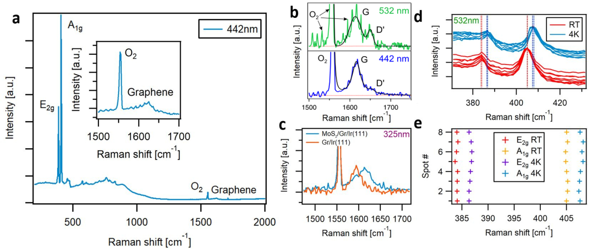
Raman spectra have been taken in the same experimental setup as the PL measurements inside a vacuum better than mbar (see Methods). Figure 4(a) shows
an overview Raman spectrum taken at 4 K using a 442 nm excitation. The related phonons with A1g and E2g symmetry are
strong in intensity compared to graphene (see inset of Figure 4(a))
and have a
splitting of 21 . A comparison of band Raman spectra for
442 nm and 532 nm excitation is shown in Figure 4(b). A shoulder at
1650 can be identified which is attributed to the band
because its intensity is changing with laser energy [46, 47], as one can see from Figure 4(b).
The appearance of the Raman band is ascribed to translational symmetry breaking by the
islands (see the STM image in Figure 1(a)) which act as
scattering centers for graphene electrons. Importantly, the graphene band prior to synthesis is
not visible by 442 nm and 532 nm excitation. [48] However, it can be
detected using UV excitation (325nm). The comparison of UV Raman spectra for
Gr/Ir(111) and the /Gr/Ir(111) heterostructure are shown
in Figure 4(c). A shift of band position from 1593
(Gr/Ir) to 1613 (/Gr/Ir) can be seen. The frequency upshift by 20 can be explained by two effects that take place after growth of MoS2. First, graphene becomes p-doped (that we have analyzed by ARPES). The band frequency upshift upon p-doping has been reported in the literature. [49, 50, 51, 48] For the observed hole concentration of an upshift from the position of charge neutral graphene by 18 is predicted. [50] Neglecting the small initial p-doping of Gr/Ir(111), this is in very good agreement to the observed 20 upshift. Notably, the precise value of the upshift depends also on the substrate and other works report values in the range of 5-10 (Refs. [49, 51, 48]). Second, we believe that, after MoS2 growth, Gr on Ir(111) becomes flatter which leads to compressive strain in Gr. This is corroborated by the fact that the Gr/Ir(111) moiré spots in the LEED pattern become weaker after MoS2 growth. The wavyness of the moiré can help to relax some of the strain in the Gr/Ir(111) system. However, after MoS2 growth, as Gr becomes flatter, it also acquires compressive strain which is known to cause an upshift in the band frequency [49, 52].
Let us now move to the investigation of temperature induced strain in the heterostructure. Raman spectroscopy is a well suited tool to investigate the change of bond length due to strain via the frequency change of Raman active vibrations. The information of that frequency change versus temperature yields information on how strongly bonded graphene and are to each other and to the substrate. For example, if both layers would follow the thermal expansion of the Ir substrate, we can assume that they are strongly bonded to each other. For graphene which is in direct contact to the Ir surface and fully covering it, one might expect that the C-C bond length follows the thermal expansion of the bulk Ir. However, the situation of MoS2 is less obvious because it is not in direct contact to the Ir and not a complete monolayer which can make it easier to maintain a thermal expansion coefficient of its own. Figure 4(d) depicts scans at several spots on the sample performed at RT and at 4 K. It can be seen that, upon cooling the phonons harden by 2.7 (the A1g mode) and by 2.6 (the E2g mode). The temperature dependent phonon frequency is phenomenologically described as where is the frequency shift and is a phonon shift per Kelvin. For there is a consensus in the literature that [42, 53, 54] (see Table 1). Interestingly, this number is largely independent of the substrate and holds also for freestanding layers [44]. It is approximately the same for both A1g and E2g phonon modes. Plugging in 290 K, we would expect a shift by 3.5 for freestanding MoS2 which is close to explaining the experimental value, but not in perfect agreement with the measured 2.6 cm-1. Considering alternative scenarios, the other extremum is strongly substrate bound . In this case, the phonon shift is dictated by the temperature induced substrate strain caused by the change of the substrate lattice parameter, to which MoS2 would be pinned. This strain can be derived from the linear thermal expansion coefficient of iridium [55, 56]. We proceed by first applying this analysis to the graphene band and then to MoS2. The strain and the phonon shift are linked to each other via the Grüneisen parameter and the phonon mode degeneracy as . Here is the phonon frequency of the unstrained system. The temperature induced strain for the Ir substrate yields . Plugging this into the above equation for the graphene mode with E2g symmetry and using , , we obtain (in Ref. [48] this analysis has been performed for the first time for Gr/Ir(111) and more details can be found there). Importantly, the temperature dependent upshift in upon cooling for the band is in good agreement to the experiment. This implies that graphene is pinned to the Ir substrate [48].
Performing the same estimation for we try to obtain a value for the temperature dependent phonon energy shift. The Grüneisen parameters of monolayer are reported in the literature as and (Ref. [41]). If we now apply the above formula, assuming that is that of the strained Ir substrate, we find and . This does not agree with experiment at all. Notably, also using the Grüneisen parameter of bulk MoS2 ( and from Ref. [45]) would not improve agreement. We thus conclude that does not follow the thermal expansion of Ir and its behaviour is better described by the expansion expected for a freestanding monolayer. Graphene, however, is stronger interacting with the Ir substrate and its Raman shift as a function of temperature can be fully understood by the thermal expansion of the substrate.
3 Conclusion and Outlook
We have characterized the epitaxially grown MoS2/Gr/Ir(111) system combining XPS, ARPES, Raman and PL measurements. STM, LEED and XPS confirm the good quality of our grown samples. We have observed a PL-signal with small FWHM suggesting a long excitonic lifetime. This surprising result is the first clear observation of photoluminescence of epitaxially grown MoS2 on a metallic substrate. The absence of the expected quenching of the PL intensity on a metallic surface can potentially be explained by a weak interaction between the epitaxial MoS2 and the substrate as is suggested by our XPS, ARPES and temperature dependent Raman measurements. Using Li deposition, we induced doping of MoS2 into a degenerate semiconductor and obtained from the analysis of ARPES data the band gap of Li-doped MoS2. Using theoretical calculations on the band gap renormalization due to doping, we estimate an exciton binding energy of 480 meV. Our results suggest that the MoS2-islands are only weakly interacting with the Gr/Ir surface which could explain the absence of quenching, but the microscopic mechanisms are still unclear. Theoretical calculations for the Dexter- and Förster-type energy transfer from the islands into the graphene substrate are thus needed to quantitatively explain the observed PL. With this background it would be interesting to grow MoS2 on hexagonal boron nitride (h-BN) using the same method as used for this work and compare FWHM and intensity of the PL. Indeed, previous experiments on h-BN capped MoS2 [8] have shown an increase in the PL intensity upon h-BN encapsulation. Similarly, it was shown that chemical treatment of flakes via an organic superacid increased PL quantum yield to near unity [57], similar treatment of epitaxially grown MoS2 monolayers might increase PL intensity even more. Additionally a transfer of MoS2 islands grown on Gr/Ir(111) onto different substrates could help to understand the effects of the substrate on the luminescent properties.
4 Appendix / supporting information
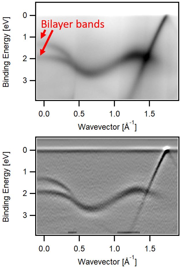
4.1 ARPES of bilayer MoS2
Figure 5 depicts ARPES spectra of bilayer MoS2 that has been grown by doubling the deposited amount of Mo. This resulted in 1.4 monolayers (ML) of MoS2 but growth conditions were specifically tuned to induce bilayer growth via sulfur pressure in the chamber and cycled growth (see Methods section). It is clear from ARPES that the VB maximum is not at the point but at the point (note the splitting of the band at into two subbands, one with a higher binding energy of approximately 1.9 eV and one with a lower binding energy of approximately 1.3 eV).
5 Methods
5.1 X-ray photoemission spectroscopy
XPS was performed at the German-Russian beamline (RGBL) of the HZB BESSY II synchrotron in Berlin (Germany) with a beam energy of 650 eV and pass energy of 20 eV in a normal emission geometry. The MoS2/Gr/Ir(111) samples were prepared in-situ and measured in a vacuum better than mbar.
5.2 Angle-resolved photoemission spectroscopy
ARPES was performed at the BaDElPh beamline [58] of the Elettra synchrotron in Trieste (Italy) with linear s- and p- polarisation at eV at temperatures of 20 K. The MoS2/Gr/Ir(111) samples were prepared in-situ and measured in a vacuum better than mbar. Li deposition was carried out in an ultra-high vacuum (UHV) chamber from SAES getters with the sample at 20 K. We performed stepwise evaporation of Li which we monitored by ARPES measurements of the band structure. Li evaporation was stopped after the desired doping level was reached.
5.3 Scanning Tunneling Spectroscopy and Microscopy
Scanning tunneling microscopy was conducted in a home built variable temperature STM apparatus in Cologne at a base pressure below mbar. For image processing the software WSxM was used [59].
5.4 Growth
We employ molecular beam epitaxy via a two-step process [13]: In the
first step, with the sample held at room temperature, Mo is evaporated at a rate of
atoms m-2 s-1 into a S background pressure of
mbar onto Gr/Ir(111). The elemental S background atmosphere
is achieved by heating a pyrite (FeS2) filled crucible to 500 K. During
the second step, the sample is annealed for 300 s at K in a S pressure of
mbar. These two steps constitute one growth cycle.
To obtain a MoS2 layer with orientation epitaxy even for coverages beyond 0.4 ML the
total coverage was deposited in subsequent growth cycles each yielding a coverage of
ML MoS2. Using this technique we realized two cycle MoS2 samples
(nominal coverage 0.7 ML) and four cycle MoS2 samples (nominal coverage 1.4 ML).
5.5 Ultra-high Vacuum Raman and photoluminescence spectroscopy
UHV Raman measurements were performed in the back-scattering geometry using commercial Raman systems (Renishaw) integrated in a homebuilt optical chamber [27], where the exciting and Raman scattered light were coupled into the vacuum using a 50x long-working distance microscope objective with an NA of 0.4 and a focal distance of 20.5 mm for lasers with wavelength 442 nm and 532 nm. For the UV laser, a UV compatible microscope objective has been used. The x UV objective has a focal distance equal to 13 mm and an NA=0.32. A sketch of our experimental setup is shown in a previous work [27]. Power densities in the range of of 100 kW/cm2 have been employed for all laser energies. The position of the laser on the sample could be checked by a camera in the laser path. All spectra have been calibrated in position and intensity to the O2 vibration at 1555 cm-1 [60].
6 Acknowledgements
N.E., J.H., A.H., T.M. and A.G. acknowledge support through the CRC 1238 within project A01. N.E., B.V.S., M.H. and A.G. acknowledge the ERC grant no. 648589 ’SUPER-2D’ and funding from DFG projects GR 3708/2-1. A.G. acknowledges INST 216/808-1 FUGG and support from the “Quantum Matter and Materials” (QM2) initiative. N.E., M.H, J.L and A.G. acknowledge support from CALIPSOplus and CERIC-ERIC for their stay at ELETTRA sincrotrone.
References
References
- [1] Kin Fai Mak, Changgu Lee, James Hone, Jie Shan, and Tony F. Heinz. Atomically thin MoS2: A new direct-gap semiconductor. Physical Review Letters, 105:136805, 2010.
- [2] Sajedeh Manzeli, Dmitry Ovchinnikov, Diego Pasquier, Oleg V. Yazyev, and Andras Kis. 2D transition metal dichalcogenides. Nature Reviews Materials, 2:17033–, June 2017.
- [3] Gang Wang, Alexey Chernikov, Mikhail M. Glazov, Tony F. Heinz, Xavier Marie, Thierry Amand, and Bernhard Urbaszek. Excitons in atomically thin transition metal dichalcogenides. Reviews of Modern Physics, 90(2):21001, 2017.
- [4] Manish Chhowalla, Hyeon Suk Shin, Goki Eda, Lain-Jong Li, Kian Ping Loh, and Hua Zhang. The chemistry of two-dimensional layered transition metal dichalcogenide nanosheets. Nature Chemistry, 5:263–, March 2013.
- [5] B. Radisavljevic, A. Radenovic, J. Brivio, V. Giacometti, and A. Kis. Single-layer MoS2 transistors. Nature Nanotechnology, 6:147–, January 2011.
- [6] Der-Hsien Lien, Matin Amani, Sujay B. Desai, Geun Ho Ahn, Kevin Han, Jr-Hau He, Joel W. Ager, Ming C. Wu, and Ali Javey. Large-area and bright pulsed electroluminescence in monolayer semiconductors. Nature Communications, 9(1):1229, 2018.
- [7] Jonghwan Kim, Chenhao Jin, Bin Chen, Hui Cai, Tao Zhao, Puiyee Lee, Salman Kahn, Kenji Watanabe, Takashi Taniguchi, Sefaattin Tongay, Michael F. Crommie, and Feng Wang. Observation of ultralong valley lifetime in WSe2/MoS2 heterostructures. Science Advances, 3(7), 2017.
- [8] F. Cadiz, E. Courtade, C. Robert, G. Wang, Y. Shen, H. Cai, T. Taniguchi, K. Watanabe, H. Carrere, D. Lagarde, M. Manca, T. Amand, P. Renucci, S. Tongay, X. Marie, and B. Urbaszek. Excitonic linewidth approaching the homogeneous limit in MoS2-based van der Waals heterostructures. Physical Review X, 7(2):1–12, 2017.
- [9] Signe S. Grønborg, Søren Ulstrup, Marco Bianchi, Maciej Dendzik, Charlotte E. Sanders, Jeppe V. Lauritsen, Philip Hofmann, and Jill A. Miwa. Synthesis of Epitaxial Single-Layer MoS2 on Au(111). Langmuir, 31:9700, 2015.
- [10] Harsh Bana, Elisabetta Travaglia, Luca Bignardi, Paolo Lacovig, Charlotte E Sanders, Maciej Dendzik, Matteo Michiardi, Marco Bianchi, Daniel Lizzit, Francesco Presel, Dario De Angelis, Nicoleta Apostol, Pranab Kumar Das, Jun Fujii, Ivana Vobornik, Rosanna Larciprete, Alessandro Baraldi, Philip Hofmann, and Silvano Lizzit. Epitaxial growth of single-orientation high-quality MoS2 monolayers. 2D Materials, 5:035012, 2018.
- [11] Jill A. Miwa, Søren Ulstrup, Signe G. Sørensen, Maciej Dendzik, Antonija Grubišić Čabo, Marco Bianchi, Jeppe Vang Lauritsen, and Philip Hofmann. Electronic structure of epitaxial single-layer MoS2. Physical Review Letters, 114(4):1–5, 2015.
- [12] Deyi Fu, Xiaoxu Zhao, Yu-Yang Zhang, Linjun Li, Hai Xu, A-Rang Jang, Seong In Yoon, Peng Song, Sock Mui Poh, Tianhua Ren, Zijing Ding, Wei Fu, Tae Joo Shin, Hyeon Suk Shin, Sokrates T. Pantelides, Wu Zhou, and Kian Ping Loh. Molecular beam epitaxy of highly crystalline monolayer molybdenum disulfide on hexagonal boron nitride. Journal of the American Chemical Society, 139(27):9392–9400, 2017.
- [13] Joshua Hall, Borna Pielić, Clifford Murray, Wouter Jolie, Tobias Wekking, Carsten Busse, Marko Kralj, and Thomas Michely. Molecular beam epitaxy of quasi-freestanding transition metal disulphide monolayers on van der waals substrates: a growth study. 2D Materials, 5(2):025005, 2018.
- [14] Guillaume Froehlicher, Etienne Lorchat, and Stéphane Berciaud. Charge Versus Energy Transfer in Atomically Thin Graphene-Transition Metal Dichalcogenide van der Waals Heterostructures. Physical Review X, 8(1):1–15, 2018.
- [15] Wouter Jolie, Clifford Murray, Phillip S. Weiß, Joshua Hall, Fabian Portner, Nicolae Atodiresei, Arkady V. Krasheninnikov, Carsten Busse, Hannu-Pekka Komsa, Achim Rosch, and Thomas Michely. Luttinger liquid in a box: electrons confined within mos2 mirror twin boundaries. not yet published, 2018.
- [16] P A Young. Lattice parameter measurements on molybdenum disulphide. Journal of Physics D: Applied Physics, 1(7):936–938, 1968.
- [17] Albert Bruix, Henrik Gøbel Füchtbauer, Anders K. Tuxen, Alexander S. Walton, Mie Andersen, Søren Porsgaard, Flemming Besenbacher, Bjørk Hammer, and Jeppe V. Lauritsen. In situ detection of active edge sites in single-layer MoS2 catalysts. ACS Nano, 9(9):9322–9330, 2015.
- [18] Hernan G. Sanchez Casalongue, Jesse D. Benck, Charlie Tsai, Rasmus K. B. Karlsson, Sarp Kaya, May Ling Ng, Lars G. M. Pettersson, Frank Abild-Pedersen, J. K. Nørskov, Hirohito Ogasawara, Thomas F. Jaramillo, and Anders Nilsson. Operando characterization of an amorphous molybdenum sulfide nanoparticle catalyst during the hydrogen evolution reaction. The Journal of Physical Chemistry C, 118(50):29252–29259, nov 2014.
- [19] Marko Kralj, Ivo Pletikosić, Marin Petrović, Petar Pervan, Milorad Milun, Alpha T. N’Diaye, Carsten Busse, Thomas Michely, Jun Fujii, and Ivana Vobornik. Graphene on ir(111) characterized by angle-resolved photoemission. Physical Review B, 84(7), 2011.
- [20] I. Pletikosić, M. Kralj, P. Pervan, R. Brako, J. Coraux, A. T. N’Diaye, C. Busse, and T. Michely. Dirac cones and minigaps for graphene on Ir(111). Physical Review Letters, 102:056808, Feb 2009.
- [21] Elena Starodub, Aaron Bostwick, Luca Moreschini, Shu Nie, Farid El Gabaly, Kevin F. McCarty, and Eli Rotenberg. In-plane orientation effects on the electronic structure, stability, and raman scattering of monolayer graphene on ir(111). Physical Review B, 83(12), mar 2011.
- [22] D. Nasr Esfahani, O. Leenaerts, H. Sahin, B. Partoens, and F. M. Peeters. Structural transitions in monolayer mos2 by lithium adsorption. J. Phys. Chem. C, 119(19):10602–10609, May 2015.
- [23] Yuanliao Zheng, Yan Huang, Haibo Shu, Xiaohao Zhou, Jiayi Ding, Xiaoshuang Chen, and Wei Lu. The effect of lithium adsorption on the formation of 1T-MoS2 phase based on first-principles calculation. Physics Letters A, 380(20):1767–1771, apr 2016.
- [24] Wenshu Chen, Jiajun Gu, Qinglei Liu, Ruichun Luo, Lulu Yao, Boya Sun, Wang Zhang, Huilan Su, Bin Chen, Pan Liu, and Di Zhang. Quantum dots of 1T phase transitional metal dichalcogenides generated via electrochemical li intercalation. ACS Nano, 12(1):308–316, 2018.
- [25] Hai He, Pengfei Lu, Liyuan Wu, Chunfang Zhang, Yuxin Song, Pengfei Guan, and Shumin Wang. Structural properties and phase transition of na adsorption on monolayer MoS2. Nanoscale Research Letters, 11(1), 2016.
- [26] T. Eknapakul, P. D. C. King, M. Asakawa, P. Buaphet, R.-H. He, S.-K. Mo, H. Takagi, K. M. Shen, F. Baumberger, T. Sasagawa, S. Jungthawan, and W. Meevasana. Electronic structure of a quasi-freestanding mos2 monolayer. Nano Letters, 14(3):1312–1316, March 2014.
- [27] A. Grüneis, B.V. Senkovskiy, A.V. Fedorov, M. Hell, and S. Michel. Ultrahigh vacuum optical spectroscopy of chemically functionalized graphene nanoribbons. In Reference Module in Chemistry, Molecular Sciences and Chemical Engineering, pages –. Elsevier, 2017.
- [28] Catalin D. Spataru and François Léonard. Tunable band gaps and excitons in doped semiconducting carbon nanotubes made possible by acoustic plasmons. Physical Review Letters, 104:177402, Apr 2010.
- [29] Holger Hartleb, Florian Späth, and Tobias Hertel. Evidence for strong electronic correlations in the spectra of gate-doped single-wall carbon nanotubes. ACS Nano, 9(10):10461–10470, 2015. PMID: 26381021.
- [30] Boris V. Senkovskiy, Alexander V. Fedorov, Danny Haberer, Mani Farjam, Konstantin A. Simonov, Alexei B. Preobrajenski, Niels Mårtensson, Nicolae Atodiresei, Vasile Caciuc, Stefan Blügel, Achim Rosch, Nikolay I. Verbitskiy, Martin Hell, Daniil V. Evtushinsky, Raphael German, Tomas Marangoni, Paul H. M. van Loosdrecht, Felix R. Fischer, and Alexander Grüneis. Semiconductor-to-metal transition and quasiparticle renormalization in doped graphene nanoribbons. Adv. Electron. Mater., 3(4):1600490, 2017.
- [31] Shiyuan Gao, Yufeng Liang, Catalin D. Spataru, and Li Yang. Dynamical excitonic effects in doped two-dimensional semiconductors. Nano Letters, 16(9):5568–5573, September 2016.
- [32] Yufeng Liang and Li Yang. Carrier plasmon induced nonlinear band gap renormalization in two-dimensional semiconductors. Physical Review Letters, 114:063001, Feb 2015.
- [33] Miguel M. Ugeda, Aaron J. Bradley, Su-Fei Shi, Felipe H. da Jornada, Yi Zhang, Diana Y. Qiu, Wei Ruan, Sung-Kwan Mo, Zahid Hussain, Zhi-Xun Shen, Feng Wang, Steven G. Louie, and Michael F. Crommie. Giant bandgap renormalization and excitonic effects in a monolayer transition metal dichalcogenide semiconductor. Nature Materials, 13:1091–, 2014.
- [34] Soohyung Park, Niklas Mutz, Thorsten Schultz, Sylke Blumstengel, Ali Han, Areej Aljarb, Lain-Jong Li, Emil J W List-Kratochvil, Patrick Amsalem, and Norbert Koch. Direct determination of monolayer MoS2 and WSe2 exciton binding energies on insulating and metallic substrates. 2D Materials, 5(2):025003, 2018.
- [35] Eva A. A. Pogna, Margherita Marsili, Domenico De Fazio, Stefano Dal Conte, Cristian Manzoni, Davide Sangalli, Duhee Yoon, Antonio Lombardo, Andrea C. Ferrari, Andrea Marini, Giulio Cerullo, and Deborah Prezzi. Photo-induced bandgap renormalization governs the ultrafast response of single-layer MoS2. ACS Nano, 10(1):1182–1188, January 2016.
- [36] Nils Krane, Christian Lotze, Julia M. Läger, Gaël Reecht, and Katharina J. Franke. Electronic structure and luminescence of quasi-freestanding MoS2 nanopatches on au(111). Nano Letters, 16(8):5163–5168, 2016.
- [37] L. Gaudreau, K. J. Tielrooij, G. E. D. K. Prawiroatmodjo, J. Osmond, F. J. GarcÃfÂa de Abajo, and F. H. L. Koppens. Universal distance-scaling of nonradiative energy transfer to graphene. Nano Letters, 13(5):2030–2035, 2013. PMID: 23488979.
- [38] FranÃf§ois Federspiel, Guillaume Froehlicher, Michel Nasilowski, Silvia Pedetti, Ather Mahmood, Bernard Doudin, Serin Park, Jeong-O Lee, David Halley, BenoÃf®t Dubertret, Pierre Gilliot, and StÃf©phane Berciaud. Distance dependence of the energy transfer rate from a single semiconductor nanostructure to graphene. Nano Letters, 15(2):1252–1258, February 2015.
- [39] Ermin Malic, Heiko Appel, Oliver T. Hofmann, and Angel Rubio. Förster-induced energy transfer in functionalized graphene. Journal of Physical Chemistry C, 118(17):9283–9289, 2014.
- [40] Changgu Lee, Hugen Yan, Louis E. Brus, Tony F. Heinz, James Hone, and Sunmin Ryu. Anomalous lattice vibrations of single- and few-layer MoS2. ACS Nano, 4(5):2695–2700, May 2010.
- [41] C. Rice, R. J. Young, R. Zan, U. Bangert, D. Wolverson, T. Georgiou, R. Jalil, and K. S. Novoselov. Raman-scattering measurements and first-principles calculations of strain-induced phonon shifts in monolayer MoS2. Physical Review B - Condensed Matter and Materials Physics, 87(8):1–5, 2013.
- [42] Satyaprakash Sahoo, Anand P. S. Gaur, Majid Ahmadi, Maxime J.-F. Guinel, and Ram S. Katiyar. Temperature-dependent raman studies and thermal conductivity of few-layer MoS2. The Journal of Physical Chemistry C, 117(17):9042–9047, 2013.
- [43] Sina Najmaei, Pulickel M. Ajayan, and J. Lou. Quantitative analysis of the temperature dependency in Raman active vibrational modes of molybdenum disulfide atomic layers. Nanoscale, 5(20):9758–9763, 2013.
- [44] Rusen Yan, Jeffrey R. Simpson, Simone Bertolazzi, Jacopo Brivio, Michael Watson, Xufei Wu, Andras Kis, Tengfei Luo, Angela R. Hight Walker, and Huili Grace Xing. Thermal conductivity of monolayer molybdenum disulfide obtained from temperature-dependent raman spectroscopy. ACS Nano, 8(1):986–993, January 2014.
- [45] S. Sugai and T. Ueda. High-pressure raman spectroscopy in the layered materials -MoS2, -MoSe2, and -MoTe2. Physical Review B, 26:6554–6558, Dec 1982.
- [46] L. G. Cançado, K. Takai, T. Enoki, M. Endo, Y. A. Kim, H. Mizusaki, A. Jorio, L. N. Coelho, R. Magalhães-Paniago, and M. A. Pimenta. General equation for the determination of the crystallite size La of nanographite by Raman spectroscopy. Applied Physics Letters, 88(16):163106, 2006.
- [47] M. A. Pimenta, G. Dresselhaus, M. S. Dresselhaus, L. G. Cançado, A. Jorio, and R. Saito. Studying disorder in graphite-based systems by Raman spectroscopy. Phys. Chem. Chem. Phys., 9:1276–1290, 2007.
- [48] Martin et al. Hell. Resonance Raman spectrum of doped epitaxial graphene at the Lifshitz transition. submitted, 2018.
- [49] Michele Lazzeri and Francesco Mauri. Nonadiabatic kohn anomaly in a doped graphene monolayer. Physical Review Letters, 97(26):266407, 2006.
- [50] A. Das, S. Pisana, B. Chakraborty, S. Piscanec, S. K. Saha, U. V. Waghmare, K. S. Novoselov, H. R. Krishnamurthy, A. K. Geim, A. C. Ferrari, and A. K. Sood. Monitoring dopants by raman scattering in an electrochemically top-gated graphene transistor. Nature Nanotechnology, 3:210–, March 2008.
- [51] Chi-Fan Chen, Cheol-Hwan Park, Bryan W. Boudouris, Jason Horng, Baisong Geng, Caglar Girit, Alex Zettl, Michael F. Crommie, Rachel A. Segalman, Steven G. Louie, and Feng Wang. Controlling inelastic light scattering quantum pathways in graphene. Nature, 471:617–, March 2011.
- [52] T. M. G. Mohiuddin, A. Lombardo, R. R. Nair, A. Bonetti, G. Savini, R. Jalil, N. Bonini, D. M. Basko, C. Galiotis, N. Marzari, K. S. Novoselov, A. K. Geim, and A. C. Ferrari. Uniaxial strain in graphene by raman spectroscopy: peak splitting, Grüneisen parameters, and sample orientation. Phys. Rev. B, 79:205433, May 2009.
- [53] Liqin Su, Yong Zhang, Yifei Yu, and Linyou Cao. Dependence of coupling of quasi 2-D MoS2 with substrates on substrate types, probed by temperature dependent Raman scattering. Nanoscale, 6(9):4920–4927, 2014.
- [54] Tianqi Yang, Xiaoting Huang, Hong Zhou, Guangheng Wu, and Tianshu Lai. Excitation mechanism of A1g mode and origin of nonlinear temperature dependence of Raman shift of CVD-grown mono- and few-layer MoS_2 films. Optics Express, 24(11):12281, 2016.
- [55] G. K. White and A. T. Pawlowicz. Thermal expansion of rhodium, iridium, and palladium at low temperatures. Journal of Low Temperature Physics, 2(5):631–639, Jun 1970.
- [56] J. J. Halvorson and R. T. Wimber. Thermal expansion of iridium at high temperatures. Journal of Applied Physics, 43(6):2519–2522, 1972.
- [57] M. Amani, D.-H. Lien, Daisuke Kiriya, J. Xiao, A. Azcatl, J. Noh, Surabhi R Madhvapathy, R. Addou, S. KC, M. Dubey, K. Cho, R. M. Wallace, S.-C. Lee, J.-H. He, J. W. Ager, X. Zhang, E. Yablonovitch, and A. Javey. Near-unity photoluminescence quantum yield in MoS2. Science, 350(6264):1065–1068, 2015.
- [58] L. Petaccia, P. Vilmercati, S. Gorovikov, M. Barnaba, A. Bianco, D. Cocco, C. Masciovecchio, and A. Goldoni. Bad elph: A normal-incidence monochromator beamline at elettra. Nuclear Instruments and Methods in Physics Research Section A: Accelerators, Spectrometers, Detectors and Associated Equipment, 606(3):780–784, 2009.
- [59] I. Horcas, R. Fernandez, J.M. Gomez-Rodriguez, J. Colchero, J. Gomez-Herrero, and A.M. Baro. Wsxm: A software for scanning probe microscopy and a tool for nanotechnology. Review of Scientific Instruments, 78(1):013705, 2007.
- [60] Gregory W. Faris and Richard A. Copeland. Ratio of oxygen and nitrogen raman cross sections in the ultraviolet. Appl. Opt., 36(12):2684–2685, Apr 1997.