Irradiation induced modification of the superconducting properties of heavily boron doped diamond
Abstract
Diamond, a wide band-gap semiconductor, can be engineered to exhibit superconductivity when doped heavily with boron. The phenomena has been demonstrated in samples grown by chemical vapour deposition where the boron concentration exceeds the critical concentration for the metal-to-insulator transition of . While the threshold carrier concentration for superconductivity is generally well established in the literature, it is unclear how well correlated higher critical temperatures are with increased boron concentration. Previous studies have generally compared several samples grown under different plasma conditions, or on substrates having different crystallographic orientations, in order to vary the incorporation of boron into the lattice. Here, we present a study of a single sample with unchanging boron concentration, and instead modify the charge carrier concentration by introducing compensating defects via high energy ion irradiation. Superconductivity is completely suppressed when the number of defects is sufficient to compensate the hole concentration to below threshold. Furthermore, we show it is possible to recover the superconductivity by annealing the sample in vacuum to remove the compensating defects.
|
|
|
|
|
|
|
||||||||||||||
| 0 | 0 | 0 | 8 | - | 3.85 | 0.998 | ||||||||||||||
| 8 | - | 3.82 | 1.003 | |||||||||||||||||
| 8 | - | 3.97 | 0.967 | |||||||||||||||||
| 8 | - | 3.86 | 0.991 | |||||||||||||||||
| 7.7 | - | 3.66 | 1.019 | |||||||||||||||||
| 7.3 | - | 3.50 | 1.015 | |||||||||||||||||
| 6 | - | 3.12 | 0.953 | |||||||||||||||||
| - | - | 1.70 | 0.730 | |||||||||||||||||
| - | - | - | 4 | 1150 | 6.68 | 0.593 | ||||||||||||||
| - | - | - | 2.2 | 1250 | 6.85 | 0.220 |
I Introduction
Superconductivity in boron doped diamond has been a topic of great interest since its discovery in 2004Ekimov et al. (2004), with the phenomena having since been reported in both single-crystal and polycrystalline samples grown by the High Pressure High Temperature (HPHT) and Chemical Vapor Deposition (CVD) methods. A wealth of experimental and theoretical investigations of the C:B system exist in the literature, ranging from transport measurements and fundamental materials science of the normal- and superconducting phase of the material, to investigations of novel non-diamond phases of carbon such as superconducting Q-carbonBhaumik et al. (2017). The exceptional physical properties of diamond, coupled with its robust superconducting properties, have motivated numerous applications to devices, including delta doped superlattice structures yielding visible light Bragg mirrors Fiori et al. (2014), diamond-based SQUID devices for magnetometry Mandal et al. (2011), and superconducting diamond nanostructures Mandal et al. (2010) and nanomechanical resonatorsBautze et al. (2014).
Initial theoretical estimates of the maximum critical temperature () of boron doped diamond were in the range of 140–160 K by virtue of the light atomic mass of the constituent atoms and strong covalent bondsMoussa and Cohen (2006). By taking into account disorder, local variations of boron concentration in the diamond lattice, and local electron-phonon coupling, the was later predicted to be as high as 55 K for boron concentration between 10-25 at. %, with signatures of superconductivity potentially appearing up to 80 K in regions of high localised orderMoussa and Cohen (2008). Yet, more than a decade of experimental work has failed to achieve a higher than 10 K, with some indication of the onset of superconductivity as high as 25 K in boron-doped diamondOkazaki et al. (2015), and 36 K in a boron doped amorphous quenched phase of carbonBhaumik et al. (2017). More recent theoretical predictions by Moussa & CohenCohen (2011) for phonon-mediated superconductors indicate the possibility that, in the ideal case, diamond could exhibit a maximum critical temperature of .
Most experimental data is well described by a standard Bardeen-Cooper-Schrieffer (BCS) model of superconductivity, with phonon-mediated Cooper pairing and a Fermi level shifted inside the valence band Winzer et al. (2005); Yokoya et al. (2005). Boron has one fewer electron than carbon, and is readily incorporated into the diamond lattice with an acceptor level at . An impurity band is formed and broadens as the concentration of isolated substitutional boron increases towards , at which point the material undergoes a transition from the semiconducting state to a metallic state, which is widely considered in the literature to coincide with the superconducting transitionKawano et al. (2010); Klein et al. (2007). Increasing the boron concentration beyond this metal-to-insulator transition (MIT) point generally corresponds to an increase in the , indicating that superconducting boron doped diamond may presently be doped sub-optimallyTakano (2009) and a further increase in the active boron concentration may yield higher . The push to experimentally realise the prediction of near room-temperature in boron-doped diamond will require the incorporation of substitutional boron at values as high as 25%. Given that equilibrium processes for growth such as HPHT are limited by the solubility of boron in diamond (approximately 2.8% Chen et al. (1999)) it is clear that non-equilibrium fabrication methods such as CVD growth and ion implantation must be pursued. Experimental data suggests that boron concentration is not the only factor in achieving superconductivity, with other authors previously observing significantly different for samples having nominally the same boron concentration - a fact attributed to improved crystallinityOkazaki et al. (2015). The crystallographic orientation of the substrate used in CVD growth also plays a role, with \hkl¡111¿ oriented diamond always resulting in higher than \hkl¡100¿ oriented diamond with the same boron concentration, which may be due to a higher concentration of electrically inactive boron dimers, or lattice strain increasing the density of states at the Fermi levelTakano (2009); Takano et al. (2007).
Recently, Bousquet et al. Bousquet et al. (2017) observed for the first time, in contrast to all previous results, that an intermediate metallic non-superconducting phase exists for boron concentrations above the MIT of , and below , corresponding to the actual critical concentration for the onset of superconductivity. This result was achieved by patterning well-defined Hall bar structures to minimise parasitic currents induced by doping inhomogeneities - i.e. percolation-like current paths through localised areas of higher boron concentration. Whereas that work involved the growth of 26 samples of differing thickness and boron concentration, here we confirm this new result by studying a single sample with fixed boron concentration and systematically compensating boron acceptors with vacancies introduced by light ion irradiation. After introducing vacancies at a density sufficient to compensate the carrier concentration to below the critical level for superconductivity, we confirm that superconductivity is quenched. We then remove the compensating defects by annealing, and show that the hole concentration and superconductivity is recovered.
II Experimental Methods
In order to gain further insight into the mechanism for superconductivity in boron doped diamond, and to determine its robustness to damage and the effect on critical temperature, an irradiation damage study of a superconducting sample was performed. A sample was grown homoepitaxially on a 33 mm Type-Ib \hkl¡111¿ oriented substrate via microwave plasma assisted CVD using the method described in several previous pubicationsKawano et al. (2010); Takano et al. (2005, 2004); Takano (2009); Takano et al. (2007); Yokoya et al. (2005). The substrate was held at 850∘C with a microwave power of 400 W and chamber pressure of 110 Torr consisting of a dilute gas mixture of methane and trimethylboron (TMB) in hydrogen. The methane concentration was 5% in hydrogen with a [TMB]/[CH4] ratio of 20,000 ppm, and growth was carried out for 20 minutes resulting in a superconducting BDD cap layer of 200 nm thickness. The as-grown sample demonstrated -type conduction, with a hole concentration of /cm3 at ambient temperature, and was measured to have a superconducting critical temperature of K and critical field in excess of 9 T. We define as the temperature at which the resistivity of the sample was reduced to 50% of its normal-state resistivity at 15 K. After growth and initial electrical characterisation, a systematic study was carried out in which the sample was repeatedly subjected to irradiation with a MeV helium ion beam, followed by electrical characterisation at cryogenic temperatures. The fluence of the ion beam was increased with each irradiation and measurement cycle, ranging between /cm2 and /cm2, at which point superconductivity was completely quenched. In each irradiation, the ion beam was raster scanned over a mm2 region, ensuring the whole sample was uniformly irradiated. The irradiation was performed with the sample held at room temperature ( K), and under vacuum of Torr, oriented ‘face on’ to the beam at a small misalignment angle of 3∘ to avoid ion channelling. During the irradiation, the sample was glued and wire-bonded into a ceramic chip carrier. Wire-bonds were made to evaporated Ti/Au electrical contact pads of thickness 100 nm and 20 nm respectively, with the bonds reinforced using a generous thickness of silver paste (300 m). The contact pads were evaporated in a typical van der Pauw configuration at the edges of the sample, having a diameter more than an order of magnitude smaller than the sample dimensions.
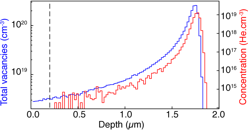
The choice of helium as the implant species was made in order to ensure the damage distribution was nominally uniform throughout the boron doped top layer, with the end-of-range of such light ions lying deep inside the substrate, well beyond the doped region. This was confirmed by modelling the Stopping and Range of Ions in Matter (SRIM) software (Figure 2). The heavy damage and amorphization of the lattice from the ions was thus placed deep in the insulating, unmeasured substrate, and only point defects from ion track damage were introduced into the superconducting surface layer. The effect of ion irradiation damage in the contact pad regions is limited to the very surface of the thick reinforcing silver paste layer, effectively shielding the evaporated ohmic contact pads and the superconducting diamond region directly underneath them. The sub-contact regions remaining unirradiated does not affect the electrical measurements, as the path of the current in the van der Pauw measurement is across the bulk irradiated sample region.
Each resultant vacancy acts as a donor which will compensate the hole introduced by a single substitutional boron atom. Thus, without changing the concentration or distribution of boron in the sample, it becomes possible to progressively compensate more and more holes until the superconductivity is quenched. The effect of the strain induced by the buried damage layer (peak depth 1.72 m) on the surface boron doped layer is not expected to be significant. Cross-sectional TEM of diamond samples implanted with high energy helium ions shows that the lattice strain is well confined around the amorphized end-of-range of the ionsFairchild et al. (2012).
After each irradiation, the sample underwent standard electrical and Hall measurements at room temperature and magnetic fields up to 0.7 T to determine resistivity, mobility, and charge carrier density. The sample was then mounted in a dilution refrigerator and cooled to approximately 50 mK while undergoing four-terminal resistance measurement using standard low noise lock-in amplifier techniques. All measurements were made in a four-terminal van der Pauw configuration using the same pair of contacts for driving current and measuring voltage each time.
III Results
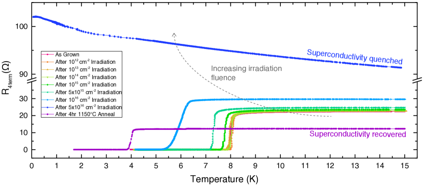
Figure 1 shows the four-terminal resistance of the sample below 15 K as a function of irradiation fluence, and Table 1 shows parameters such as irradiation fluence, defect concentration in the 200 nm superconducting cap layer as modelled by SRIM, superconducting critical temperature, and the hole concentration and mobility determined from electrical measurements. To within the error of the measurement, no change in was seen for an irradiation fluence up to /cm2. At fluences above this level, three general trends were observed:
-
1.
The bulk resistivity of the sample (measured cryogenically, above ) increased with increasing fluence,
-
2.
The superconducting decreased, as well as the charge carrier (hole) concentration ,
-
3.
The width of the superconducting transition, i.e. the difference between the onset of superconductivity and the offset (zero resistance) was broadened.
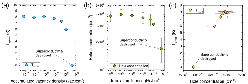
The width of the transition in particular suggests an increasingly inhomogeneous material, with the accumulated damage from the ion irradiation creating localised regions of differing defect density and nanoscale order, with a spectrum of critical temperatures. While the sample remained superconducting at 6 K after accumulating a vacancy concentration of /cm3, the final irradiation at a fluence of /cm2 led to a large increase in the resistivity of the sample and complete quenching of superconductivity above our base temperature of 50 mK. Figure 3 shows the change in as a function of accumulated vacancy density and hole concentration, and the hole concentration as a function of irradiation fluence.
The efficiency of compensation up to a fluence of /cm2, that is to say the ratio of the measured post-irradiation hole concentration to the expected concentration (pre-irradiation concentration minus the number of vacancies introduced), was very high at 97%. The final implant, with fluence /cm2, resulted in lower hole compensation efficiency of only 36%, but the reason for this is unclear. In any case, we found that progressively reducing the hole concentration in this superconducting sample also led to a reduction in , with the apparent threshold hole concentration for superconductivity lying in the range /cm3.
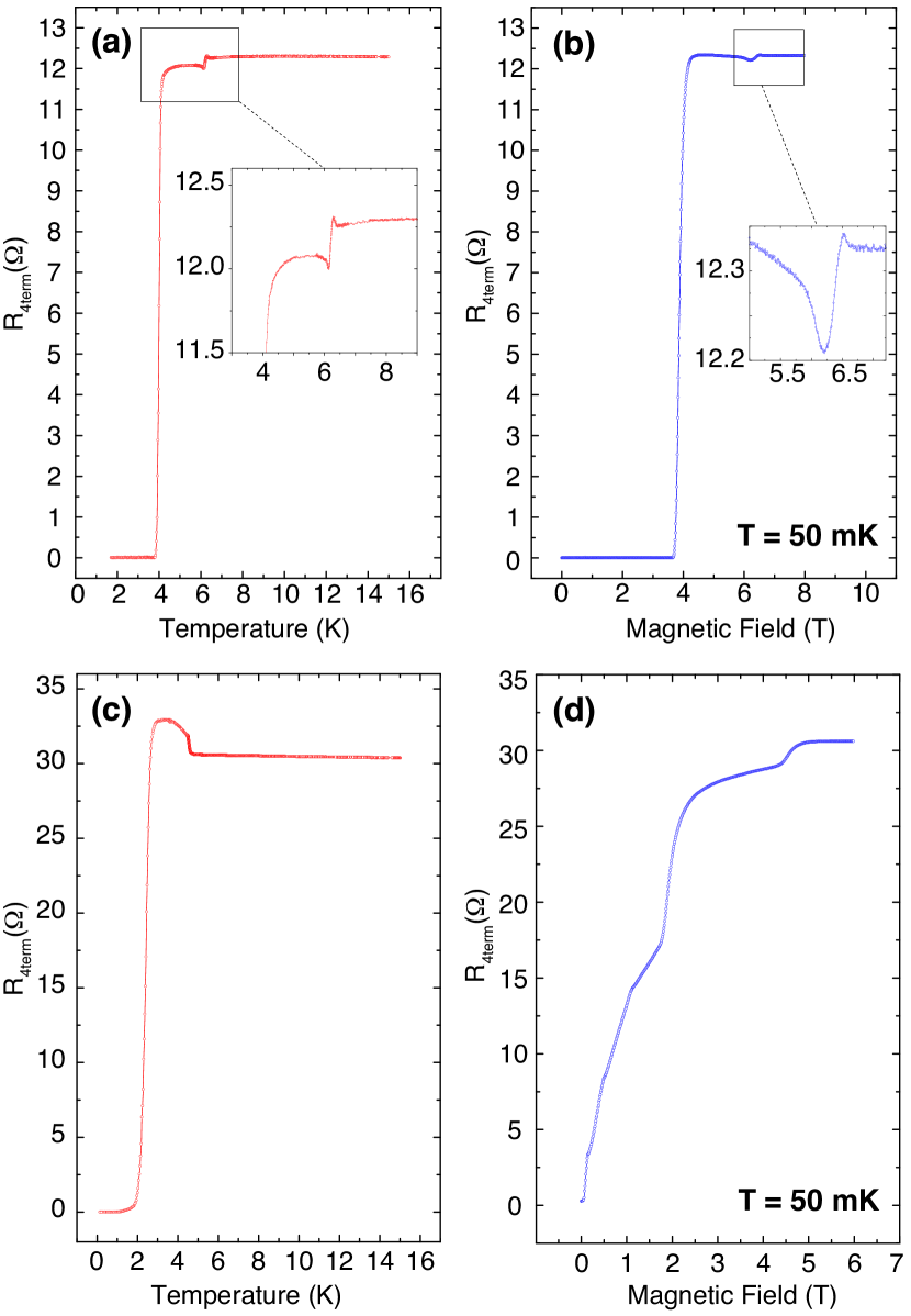
It has been shown previously that annealing diamond is an effective method of removing compensating point defectsKalish et al. (1999). To attempt to remove the point defects introduced by helium ion irradiation, the sample was annealed in vacuum at C for four hours, with a slow ramp up and ramp down from this temperature of approximately 10 hours each. After annealing, electrical measurements revealed the successful recovery of superconductivity in the sample, albeit at a lower . Figure 4(a) shows the same data as Figure 1 for the sample after annealing at 1150∘C, but with a vertically exaggerated aspect ratio in order to highlight an anomalous preliminary transition before the bulk of the material becomes superconducting. This behaviour, which was not observed at any point during the irradiation study prior to annealing, suggests that the annealing strategy catalysed the separation of the material into two discrete regions with differing . At such a low annealing temperature, boron is not mobile and will not diffuse in diamond, so the redistribution of boron into higher concentration areas is unlikely. We are left to conclude that domains or percolation paths through the material have had compensating defects annealed out with higher efficiency than the bulk, leading to part of the material undergoing a superconducting transition at a higher due to the resultant non-uniform hole density. This echoes the result of Bousquet et al. Bousquet et al. (2017) that highlights the need for well-defined conducting structures to avoid parasitic conduction paths and enable accurate determination of the critical carrier density for superconductivity.
After electrical characterisation, the sample was annealed a second time using the same protocol but at a slightly higher temperature of C. New contact pads were evaporated post-anneal and cryogenic measurement again revealed a seemingly polyphasic material, but with a lower critical temperature than after the first anneal (Figure 4(c)). The transition from the normal conducting state to superconductivity is now preceded by an initial rise in resistance, an effect which has been seen previously in boron doped granular diamondZhang et al. (2013). In that case, the effect was attributed to a small degree of disorder preventing a direct transition of the material from the metallic state into global superconductivity. Instead, the material is first tuned through a bosonic insulator phase as localised disorder and the associated spatially varying potential cause bosonic ‘islands’ of Cooper pairs to form. As the temperature is decreased, the bosonic islands grow and begin to percolate, allowing the onset of global superconductivity. Microscopic disorder has also been directly shown to cause nucleation of superconducting pairing gaps in nanoscale regions above in the high temperature superconductor Bi2Sr2CaCu2O8+δ Gomes et al. (2007). These localised islands of superconductivity proliferate as the temperature is lowered, resulting in a spatially distributed collection of domains with varying superconducting . The effect could also be indicative of that seen in disordered metals close to the MIT Osofsky et al. (2001, 2002).
Additional structure is apparent in the measurement of critical field in our sample after the second anneal (Figure 4(d)), with the field for global superconductivity heavily suppressed from that measured after the first C anneal (Figure 4(b)). As many as six partial transitions can be seen between the metallic state at the highest measured field and global superconductivity near zero field, indicating a highly non-uniform material with a distribution of regions of differing .
IV Discussion
Whereas previous work has compared CVD boron doped diamond layers of differing thickness, boron concentration, crystallographic orientation, and almost certainly differing local disorder at the nanoscale, the present work has studied a single sample of fixed boron concentration. Irradiation with high energy light ions was used to systematically compensate boron acceptors through the introduction of vacancies, with one single vacancy capable of compensating one single substitutional boron atom. Thus, the density of states at the Fermi level is reduced, and correspondingly the also decreases. Our data shows good agreement with this simple picture, with the measured concentration of acceptors (holes from substitutional boron) reduced by the accumulated number of donors (vacancies as modelled by SRIM) with each iteration of the irradiation and measurement process. At the point where the hole concentration is compensated beyond the threshold for superconductivity near the metal-to-insulator transition, superconductivity is quenched as expected.
The recovery of superconductivity in the sample after annealing, however, highlights that the relationship between active boron concentration and is not so straightforward. After annealing at 1150∘C, the measured hole density at ambient temperature is the highest recorded for this sample, approximately 75% higher than the as-grown sample with K. Yet despite the increased hole concentration, the critical temperature after annealing is only 4 K, lower than that measured at any stage of irradiation. After annealing the sample a second time at 1250∘C, the hole density increases further, though not significantly, but the critical temperature drops again to 2.2 K.
Now we must reconcile the increase in the measured hole concentration and the decrease in post-annealing, given that the amount of boron in the sample is fixed. The annealing process can have only either removed compensating defects in the sample or changed their location or bonding configuration. The increase in carrier concentration can potentially be attributed to the removal of existing compensating defects such as hydrogen in addition to the vacancies introduced during irradiation, effectively activating them electrically. However, if this was the case we would expect an increase in , up to a certain limit. Because the only inclusion which contributes carriers to superconductivity in diamond is substitutional boron, there exists a boron concentration where saturates due to boron clustering to form dimers. These dimers do not contribute to the density of states at the Fermi level, thereby reducing the value of Bhaumik et al. (2017). There is however some evidence to suggest that boron dimers can act as acceptors when incorporated at boron concentrations greater than 3% (i.e. )Bourgeois et al. (2006). Theoretical studies of boron-based defects in diamond have shown that all substitutional boron complexes act as acceptors, while complexes containing vacancies or interstitials typically act as donors which act to passivate holes in the valence bandGoss and Briddon (2006). Interstitial boron are particularly effective at passivating holes, acting as donors that can compensate up to three holes per boron atom Moussa and Cohen (2008).
Because the annealing process has increased the hole density in our sample, we conclude that the anneal acts to increase the fraction of boron located in substitutional sites without being dimerized or compensated by hydrogen or vacancy defects. This may occur either by removing or reconfiguring the defects into non-boron containing defect complexes, or by enabling interstitial or dimerized boron to become single substitutional boron. Given that boron is not mobile in diamond at the annealing temperatures used, it is more likely that the anneal acts to effectively remove compensating defects. Boron, as a substitutional impurity, could however diffuse though vacancies. The activation energy for this process is as high as 8.9 eV (the sum of the formation and migration energy), however the presence of existing defects such as the large concentration of vacancies may allow an easy parallel diffusion channelSung et al. (1995). In any case, as noted previouslyBourgeois et al. (2006) one cannot expect a simple dependence of the free carrier concentration on . The apparent disconnect between the very high hole concentration and very low in our sample post-anneal may be explained by localised disorder as discussed by Moussa et al Moussa and Cohen (2008). All valence states in boron doped diamond have strong electron-phonon coupling, and Moussa et al. suggest that the only way in which substitutional disorder can quench superconductivity is if it is strong enough to open a gap in the valence states. After annealing, our sample exhibits clear signs of local disorder such as the broadened superconducting transition, and seemingly multiphasic transitions from the metallic to globally superconducting state including something reminiscent of an intermediate bosonic-insulator phase. It should also be noted that the hole mobility drops significantly at the point where superconductivity is quenched in our sample, and further again after annealing, suggesting increased scattering of carriers by the defects introduced by the irradiation.
V Conclusion
Our results indicate a threshold carrier concentration for the onset superconductivity in boron doped diamond of between . This result is consistent with the recent findings of Bousquet et al. Bousquet et al. (2017) which show that the threshold boron concentration for superconductivity does not coincide with the metal to insulator transition. Furthermore, we show that the critical temperature of the material has reasonable robustness against irradiation damage, showing no degradation of up to fluences of , with total destruction of superconductivity at a fluences between . The fact that superconductivity can be recovered in samples of boron doped diamond which have suffered heavy irradiation damage is promising, and the parameters of the recovered sample suggest that localised disorder in superconducting boron doped diamond has a strong effect on the density of states at the Fermi level and thus the
Samples grown by plasma assisted CVD currently demonstrate the highest measured for boron doped diamond, but it remains an open question why superconductivity has not been observed in samples fabricated using high energy implantation of boron into diamond, even when doped at a concentration above the MIT thresholdHeera et al. (2008); van Beveren et al. (2016); Tsubouchi and Shikata (2012). Whilst the damage and amorphization of the lattice caused by high energy ion implantation are likely explanations for the absence of superconductivity, in-situ dynamic annealing is a promising techniqueTsubouchi et al. (2006); van Beveren et al. (2016) for preventing significant damage and maintaining the important property of high atomic order critical for high temperature superconductivityCohen (2011). Despite the use of this technique, boron implanted diamond with carrier concentration above the MIT has still not been made to superconduct.
The present result may explain the absence of superconductivity in diamond doped by high energy implantation of boron, which is likely to have a very large number of defects which passivate the boron and significant disorder due to implantation damage. Given the assertion that disorder must be high enough to open a gap in the valence states in order to quench superconductivity, future work should include angle-resolved photoemission spectroscopy (ARPES) measurements of samples irradiated with light ions, or samples fabricated via boron implantation. This direct probe of the band structure may provide further insight into how higher critical temperatures can be achieved in this promising material.
In summary, our work demonstrates for the first time the ability to directly alter the superconducting properties of diamond through ion implantation, an advance which may lead to the ability to selectively write well-defined channels or regions of normal-conducting diamond into superconducting layers, or create the Josephson junction ‘weak links’ required for SQUID devices using a focused ion beam. Such devices engineered fully from diamond are of interest due to the fact that interface and surface state noise is a major source of decoherence for superconducting resonators and quantum devicesOliver and Welander (2013). The ability to create buried superconducting diamond devices through CVD growth and subsequent ion irradiation may suppress or avoid the surface and interface noise suffered by present qubit technology which relies on metal/semiconductor or metal/dielectric heterostructures with complex material interfaces. Finally, the unique combination of thermal and mechanical properties of diamond, combined with it’s low absorption in a large transmission window ranging from ultraviolet to infrared wavelengths lend itself well to use in integrated photonic circuits. Single photon detectors based on superconducting NbN nanowires integrated into diamond-based nanophotonic circuits have shown promiseRath et al. (2015); Kahl et al. (2016), but the extremely high critical current of boron doped diamond, and the ability to grow epitaxially on diamond with lower lattice mismatch may provide performance enhancements. Using ion irradiation to define nanowire geometries could allow buried nanowires to be fabricated inside the waveguide of such photonic circuits, rather than evanescently coupled on the surface.
Acknowledgements
The authors wish to acknowledge that this research was funded by the Australian Research Council under Grant No. DP150102703, and the United States Air Force Research Laboratory under Agreement No. FA2386-13-1-4055. The U.S. Government is authorised to reproduce and distribute reprints for Governmental purposes notwithstanding any copyright notation thereon. The authors also acknowledge access to ion implantation and/or ion-beam analysis facilities at the ACT node of the Heavy Ion Accelerator Capability funded by the Australian Government under the NCRIS program.
References
- Ekimov et al. (2004) E. A. Ekimov, V. A. Sidorov, E. D. Bauer, N. N. Mel’nik, N. J. Curro, J. D. Thompson, and S. M. Stishov, “Superconductivity in diamond,” Nature 428, 542–545 (2004).
- Bhaumik et al. (2017) A. Bhaumik, R. Sachan, and J. Narayan, “High-temperature superconductivity in boron-doped Q-carbon,” ACS Nano 11, 5351–5357 (2017).
- Fiori et al. (2014) A. Fiori, J. Bousquet, D. Eon, F. Omnès, E. Bellet-Amalric, and E. Bustarret, “Boron-doped superlattices and Bragg mirrors in diamond,” Applied Physics Letters 105, 081109 (2014).
- Mandal et al. (2011) Soumen Mandal, Tobias Bautze, Oliver A. Williams, Cécile Naud, Étienne Bustarret, Franck Omnès, Pierre Rodière, Tristan Meunier, Christopher Bäuerle, and Laurent Saminadayar, “The diamond superconducting quantum interference device,” ACS Nano 5, 7144–7148 (2011).
- Mandal et al. (2010) Soumen Mandal, Cécile Naud, Oliver A Williams, Étienne Bustarret, Franck Omnès, Pierre Rodière, Tristan Meunier, Laurent Saminadayar, and Christopher Bäuerle, “Nanostructures made from superconducting boron-doped diamond,” Nanotechnology 21, 195303 (2010).
- Bautze et al. (2014) Tobias Bautze, Soumen Mandal, Oliver A. Williams, Pierre Rodière, Tristan Meunier, and Christopher Bäuerle, “Superconducting nano-mechanical diamond resonators,” Carbon 72, 100 – 105 (2014).
- Moussa and Cohen (2006) Jonathan E. Moussa and Marvin L. Cohen, “Two bounds on the maximum phonon-mediated superconducting transition temperature,” Phys. Rev. B 74, 094520 (2006).
- Moussa and Cohen (2008) Jonathan E. Moussa and Marvin L. Cohen, “Constraints on for superconductivity in heavily boron-doped diamond,” Phys. Rev. B 77, 064518 (2008).
- Okazaki et al. (2015) Hiroyuki Okazaki, Takanori Wakita, Takayuki Muro, Tetsuya Nakamura, Yuji Muraoka, Takayoshi Yokoya, Shin-ichiro Kurihara, Hiroshi Kawarada, Tamio Oguchi, and Yoshihiko Takano, “Signature of high above 25 K in high quality superconducting diamond,” Appl. Phys. Lett. 106 (2015).
- Cohen (2011) Marvin L. Cohen, “Conceptual progress for explaining and predicting semiconductor properties,” J. Mater. Res. 26, 2815–2825 (2011).
- Winzer et al. (2005) K. Winzer, D. Bogdanov, and C. Wild, “Electronic properties of boron-doped diamond on the border between the normal and the superconducting state,” Physica C 432, 65–70 (2005).
- Yokoya et al. (2005) T. Yokoya, T. Nakamura, T. Matsushita, T. Muro, Y. Takano, M. Nagao, T. Takenouchi, H. Kawarada, and T. Oguchi, “Origin of the metallic properties of heavily boron-doped superconducting diamond,” Nature 438, 647–650 (2005).
- Kawano et al. (2010) Akihiro Kawano, Hitoshi Ishiwata, Shingo Iriyama, Ryosuke Okada, Takahide Yamaguchi, Yoshihiko Takano, and Hiroshi Kawarada, “Superconductor-to-insulator transition in boron-doped diamond films grown using chemical vapor deposition,” Phys. Rev. B 82, 085318 (2010).
- Klein et al. (2007) T. Klein, P. Achatz, J. Kacmarcik, C. Marcenat, F. Gustafsson, J. Marcus, E. Bustarret, J. Pernot, F. Omnes, Bo E. Sernelius, C. Persson, A. Ferreira da Silva, and C. Cytermann, “Metal-insulator transition and superconductivity in boron-doped diamond,” Physical Review B 75, 165313 (2007).
- Takano (2009) Yoshihiko Takano, “Superconductivity in CVD diamond films,” J. Phys. Condens. Matter 21 (2009).
- Chen et al. (1999) Yung-Hsin Chen, Chen-Ti Hu, and I-Nan Lin, “Defect structure and electron field-emission properties of boron-doped diamond films,” Applied Physics Letters 75, 2857–2859 (1999).
- Takano et al. (2007) Y. Takano, T. Takenouchi, S. Ishii, S. Ueda, T. Okutsu, I. Sakaguchi, H. Umezawa, H. Kawarada, and M. Tachiki, “Superconducting properties of homoepitaxial CVD diamond,” Diam. Relat. Mat. 16, 911–914 (2007).
- Bousquet et al. (2017) J. Bousquet, T. Klein, M. Solana, L. Saminadayar, C. Marcenat, and E. Bustarret, “Phase diagram of boron-doped diamond revisited by thickness-dependent transport studies,” Phys. Rev. B 95, 161301 (2017).
- Takano et al. (2005) Y. Takano, M. Nagao, T. Takenouchi, H. Umezawa, I. Sakaguchi, M. Tachiki, and H. Kawarada, “Superconductivity in polycrystalline diamond thin films,” Diam. Relat. Mat. 14, 1936–1938 (2005).
- Takano et al. (2004) Y. Takano, M. Nagao, I. Sakaguchi, M. Tachiki, T. Hatano, K. Kobayashi, H. Umezawa, and H. Kawarada, “Superconductivity in diamond thin films well above liquid helium temperature,” Appl. Phys. Lett. 85, 2851–2853 (2004).
- Fairchild et al. (2012) Barbara A. Fairchild, Sergey Rubanov, Desmond W. M. Lau, Marc Robinson, Irene Suarez-Martinez, Nigel Marks, Andrew D. Greentree, Dougal McCulloch, and Steven Prawer, “Mechanism for the amorphisation of diamond,” Advanced Materials 24, 2024–2029 (2012).
- Kalish et al. (1999) R. Kalish, A. Reznik, K. W. Nugent, and S. Prawer, “The nature of damage in ion-implanted and annealed diamond,” Nucl. Instrum. Methods Phys. Res. Sect. B-Beam Interact. Mater. Atoms 148, 626–633 (1999).
- Zhang et al. (2013) Gufei Zhang, Monika Zeleznik, Johan Vanacken, Paul W. May, and Victor V. Moshchalkov, “Metal-bosonic insulator-superconductor transition in boron-doped granular diamond,” Phys. Rev. Lett. 110, 077001 (2013).
- Gomes et al. (2007) Kenjiro K. Gomes, Abhay N. Pasupathy, Aakash Pushp, Shimpei Ono, Yoichi Ando, and Ali Yazdani, “Visualizing pair formation on the atomic scale in the high- superconductor Bi2Sr2CaCu2O8+δ,” Nature 447, 569–572 (2007).
- Osofsky et al. (2001) M. S. Osofsky, R. J. Soulen, J. H. Claassen, G. Trotter, H. Kim, and J. S. Horwitz, “New insight into enhanced superconductivity in metals near the metal-insulator transition,” Physical Review Letters 87, 197004 (2001).
- Osofsky et al. (2002) M. S. Osofsky, R. J. Soulen, J. H. Claassen, G. Trotter, H. Kim, and J. Horwitz, “Enhanced superconductivity in metallic oxides near the metal-insulator transition,” Physical Review B 66, 020502 (2002).
- Bourgeois et al. (2006) E. Bourgeois, E. Bustarret, P. Achatz, F. Omnès, and X. Blase, “Impurity dimers in superconducting B-doped diamond: Experiment and first-principles calculations,” Physical Review B 74, 094509 (2006).
- Goss and Briddon (2006) J. P. Goss and P. R. Briddon, “Theory of boron aggregates in diamond: First-principles calculations,” Physical Review B 73, 085204 (2006).
- Sung et al. (1995) T. Sung, G. Popovici, M. A. Prelas, and R. G. Wilson, “Boron diffusion coefficient in diamond,” Materials Research Society Symposium Proceedings 416, 467–470 (1995).
- Heera et al. (2008) V. Heera, R. Hoehne, O. Ignatchik, H. Reuther, and P. Esquinazi, “Absence of superconductivity in boron-implanted diamond,” Diam. Relat. Mat. 17, 383–389 (2008).
- van Beveren et al. (2016) L. H. Willems van Beveren, R. Liu, H. Bowers, K. Ganesan, B. C. Johnson, J. C. McCallum, and S. Prawer, “Optical and electronic properties of sub-surface conducting layers in diamond created by MeV B-implantation at elevated temperatures,” J. Appl. Phys. 119 (2016).
- Tsubouchi and Shikata (2012) Nobuteru Tsubouchi and S. Shikata, “Change of structural and electrical properties of diamond with high-dose ion implantation at elevated temperatures: Dependences on donor/acceptor impurity species,” Nucl. Instrum. Methods Phys. Res. Sect. B-Beam Interact. Mater. Atoms 286, 303–307 (2012).
- Tsubouchi et al. (2006) Nobuteru Tsubouchi, Masahiko Ogura, Yuji Horino, and Hideyo Okushi, “Low-resistance layer formation into diamond using heavily B ion implantation,” Appl. Phys. Lett. 89 (2006).
- Oliver and Welander (2013) William D. Oliver and Paul B. Welander, “Materials in superconducting quantum bits,” MRS Bulletin 38, 816–825 (2013).
- Rath et al. (2015) Patrik Rath, Oliver Kahl, Simone Ferrari, Fabian Sproll, Georgia Lewes-Malandrakis, Dietmar Brink, Konstantin Ilin, Michael Siegel, Christoph Nebel, and Wolfram Pernice, “Superconducting single-photon detectors integrated with diamond nanophotonic circuits,” Light: Science & Applications 4 (2015).
- Kahl et al. (2016) Oliver Kahl, Simone Ferrari, Patrik Rath, Andreas Vetter, Christoph Nebel, and Wolfram H. P. Pernice, “High efficiency on-chip single-photon detection for diamond nanophotonic circuits,” J. Lightwave Technol. 34 (2016).