Synthesizing Cu-Sn nanowires alloy in highly-ordered Aluminum Oxide templates by using electrodeposition method
Abstract
In this research a novel and simple electrochemical method is developed in order to facilitate the large-scale production of nanowires. The proposed electrochemical technique shows versatile controllability over chemical composition and crystalline structure of Cu-Sn nanowires. Another important factor, which could be controlled by using this method, is the order structure of nanowires more accurately in comparison to conventional synthesizing procedures. As a result, the Cu-Sn nanowires as well as Aluminum Oxide templates synthesized by using the proposed electrochemical method are examined due to their morphology and chemical structure to find a relation between electrodeposition’s solution chemistry and materials properties of Cu-Sn nanowires. The results show that the proposed electrochemical method maintains a highly-ordered morphology as well as versatile controllability over chemical composition of nanowires, which could be used to optimize the procedure for industrial applications due to low cost and simple experimental setup.
keywords:
Cu-Sn nanowires, Highly-ordered Aluminum Oxide, Electrodeposition, AC electrochemical deposition, Self-assembled templates1 Introduction
Tin (Sn) based anodes are rigorously studied in order to increase the Li-ion batteries’ capacities [1, 2, 3, 4, 5, 6, 7, 8, 9, 10, 11, 12, 13, 14, 15, 16, 17, 18, 19, 20, 21, 22]. Although, large volumetric strains, during insertion/extraction, could lead to mechanical failure of anodes and reduce the cyclability of Lithium-ion batteries [23, 24, 25]. As a result, alloying the anode material (i.e. Sn) with mechanically stable elements (e.g. Ni, Co, Cu, graphene, etc.) method is developed in order to achieve promising cycling performance and utilizing the higher capacity of Tin (Sn) simultaneously [1, 2, 3, 6, 15, 12]. Furthermore, nanostructured version of these Tin based alloys (e.g. nanowires, nanoparticles, etc.) could stabilize the volumetric strains more effectively, because of their small volume changes in comparison to thin films [26]. Although, synthesizing the nanostructures in large volume for industrial applications is challenging due to their expensive and time consuming production methods, such as: surfactant based techniques or self-assembling of 0D nanostructures [27, 28, 29]. However, electrodeposition methods (e.g. direct or alternating current techniques) have shown more accurate controllability over materials morphology and chemical composition of nanostructures in comparison to conventional production techniques as well as their easier scalability for industrial applications [30, 31, 32]. Electrodeposition of metallic alloys in the ordered self-assembled templates (e.g. , , porous polycarbonate, etc.) is developed primarily to control the morphology of nanostructures [33, 34, 35, 36, 37]. The main disadvantage of conventional direct current electrodeposition methods in order to synthesize nanostructures in self-assembled templates, is the practical difficulties of producing a conductive self-assembled structure due to low conductivity of templates’ materials [38, 39, 40, 41, 42, 43, 44, 45, 46, 47, 48, 49, 50, 51]. On the other hand, alternating current (AC) electrochemical deposition method is primarily developed to overcome the technical difficulties, related to removing the barrier layer of the anodic Aluminum Oxide (AAO) and coating this self-assembled template with conductive materials [52]. As a result, the AC electrodeposition technique has a potential to facilitate the industrial scale production of nanostructures with a highly controlled morphology as well as their chemical structure [34]. In this research, AC electrochemical deposition method has been deployed to synthesize highly-ordered Cu-Sn nanowires in Aluminum Oxide templates. In the first section of this research paper, two steps anodization technique, which is used to produce a highly-ordered template, as well as its morphological properties will be discussed in details. Then morphological properties as well as chemical structure of synthesized Cu-Sn nanowires will be investigated in order to examine their crystalline structures as well as controllability of nanowires’ chemical composition. All the experiments in this research are done at room temperature, which facilitates its generalization for industrial scale applications due to technical difficulties related to costly temperature controlling systems [53].
2 Materials and methods
2.1 Two step anodizing
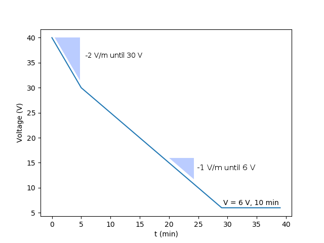
Before anodizing of planar Aluminum samples (Merck KGaA, 99.95%, 0.3 mm thickness - annealed), electrodes are electropolished () in 60 wt. % solution. In fact, the electropolishing voltage and temperature are fixed at 2 V and room temperature (C) respectively. Also, the electropolishing time is optimized at 5min in order to achieve a highly smooth surface without primary amorphous Aluminum Oxide. In both the first and second steps of anodization procedure, the electrodes are anodized in 0.3M solution. Furthermore, anodization time, voltage, and temperature are fixed at 2h, 40 V and room temperature (C) respectively for first and second steps of this anodizing procedure. Synthesized porous Aluminum Oxides after the first step of anodization are etched in a solution of 0.6M 85 wt. % - 0.2M . The etching temperature and time are fixed at C and 30min respectively. The main challenge, in order to use Aluminum Oxide templates for electrodeposition purposes directly, is how to reduce the electrical resistance of barrier layer, which prevents the electrical current flow through the thick insulative layer at the bottom of the pores (i.e. barrier layer) [54, 55, 56, 57, 58]. In this research, the barrier layer thinning (BLT) procedure (i.e. reducing the second step anodization voltage gradually), which is shown as a voltage-time plot in fig. 1 schematically, is used to reduce the electrical impedance of the Aluminum Oxide layer at the bottom of the pores. Additionally, the electrical impedance of the electrodes, before and after BLT procedure, are examined by using impedance spectroscopy.
2.2 AC nanowire electrodeposition
The AC electrochemical deposition technique is employed to reduce and ions in the pores of self-assembled Aluminum Oxide template. In all the experiments of this section, pH as well as Boric acid () concentration, root mean square (RMS) voltage, and AC signal’s frequency are fixed at 1, 0.5M, 10 V, and 200 Hz respectively. As a result, 10 samples are prepared to investigate the effect of Tin Sulfate () concentration on the chemical composition of produced nanowires. The concentration is changed from 0 to 0.5M and chemical composition as well as crystalline structure of deposited nanowires are examined by using energy dispersive spectroscopy (EDS) and X-ray diffraction respectively.
2.3 Materials characterization
Samples’ characterization, which was used to investigate morphology of self-assembled templates as well as Cu-Sn nanowires, was done with a field emission scanning electron microscope (FE-SEM) Quanta 3D FEG (FEI, Phillips, The Netherlands). In order to examine the pore sizes as well as morphology (i.e. order structure) of nanowires, ImageJ [59] image processing software is used to obtain quantitative information on the average diameter of the self-assembled templates’ pores’ diameter and length, as well as diameter of the electrodeposited Cu-Sn nanowires. The crystalline structure of the Cu-Sn nanowire alloy was analyzed by X-ray diffraction using a Rigaku Ultima IV diffractometer with Co K radiation and operating parameters of 40 mA and 40 kV with a scanning speed of per minute and step size of . Finally, the impedance spectroscopy of the anodized samples were done by using a MultiPalmSens4 potentiostat in order to compare the electrical resistance of anodizied samples before and after barrier layer thinning procedure.
3 Results and discussion
3.1 Aluminum Oxide morphology
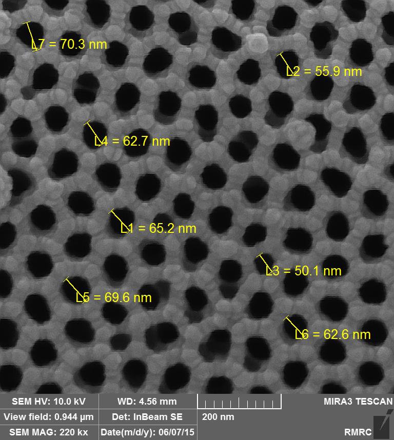
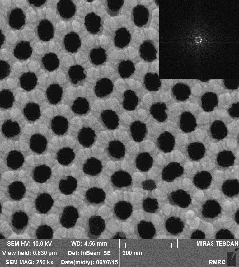
The porous morphology of two steps anodized Aluminum Oxide is shown in fig. 2. According to fig. 22(a), which is analyzed by using image processing techniques, it could be understood that the average pore size of this self-assembled template is 60 nm. Furthermore, the order structure of this porous medium is analyzed by using the fast Fourier transform (FFT) technique in order to examine the spatial structure of pores and their deviation from honeycomb structure. As a result, according to fig. 22(b), the FFT result of this AAO microstructure shows 6 strong bright dots, which indicates that a perfect honeycomb structure is achieved after the second step of anodization.
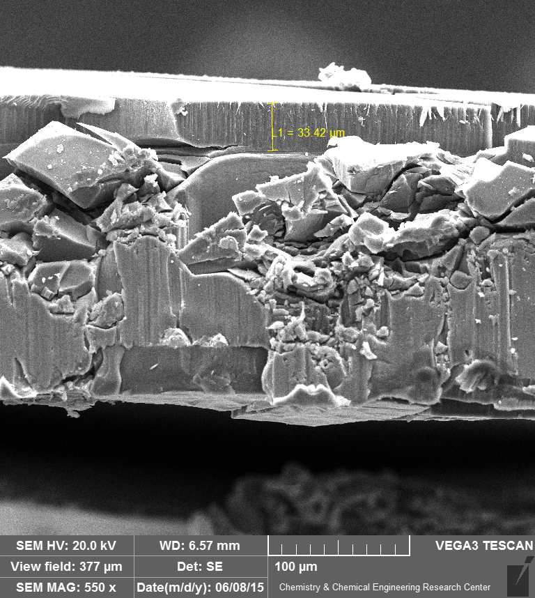
Additionally, in order to examine the aspect ratio of self-assembled pores of AAO, a cross-sectional FE-SEM microscopy is done to estimate the thickness of Aluminum Oxide after the second step of anodization (cref. fig. 3). As shown in fig. 33(a), the thickness of AAO template is about 33 m. As a result, the aspect ratio of pores, which is defined as the ratio of thickness over diameter, could be estimated as 550. Also, this aspect ratio will be increased for nanowires after AAO dissolution because of nanowires’ radial shrinkage due to compressive residual stresses [60, 61]. The wall thickness of pores in self-assembled AAO template is estimated as 60 nm, which is shown in fig. 33(b).
This highly ordered structure after the second step of anodization is achieved because: the quantum dots are created on the electrode’s surface after etching step, which could facilitate the directional growth of AAO as well as controlling of its diameter more precisely [62].
3.2 Impedance spectroscopy of Aluminum Oxide template’s barrier layer
Impedance spectroscopy is done in order to examine the electrical resistance of barrier layer before and after the thinning procedure. Additionally, the impedance of barrier layer directly could be related to its thickness as [63, 64]:
| (1) | |||
| (2) |
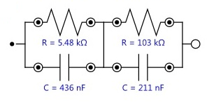
Where is the electrical impedance, is the imaginary unit, is the frequency, is frequency scattering factor, is the barrier layer capacity, is the barrier layer thickness, is the relative electrical permittivity, is the electrical permittivity of vacuum, and is the surface area of the sample. The impedance magnitude versus frequency and its real part versus imaginary part (Nyquist plot) for before and after the barrier layer thinning procedure are shown in fig. 44(a) and fig. 44(b) respectively. The equations 1 and 2 are used to fit them into the Nyquist plots (cref. fig. 4) and as a result, the obtained values for barrier layer thicknesses before and after BLT procedure are 20nm and 5nm respectively.
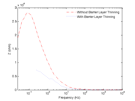
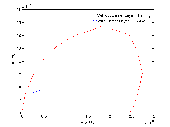
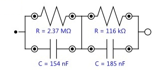
This calculation shows that the BLT procedure reduced the barrier layer thickness 4 times smaller, which could increase its conductivity and facilitate the AC electrochemical deposition step. Additionally, the electrical circuits equivalence of the Nyquist plots are extracted due to the fitted parameters which are shown in fig. 5. According to these electrical circuits, it could be understood that the second resistance/capacitance pair remained constant before and after BLT procedure. However, the electrical resistance of first resistance/capacitance pair is reduced by three orders of magnitude, which shows the electrical resistance is reduced after BLT procedure significantly (cref. fig. 5).
3.3 Cu-Sn nanowires
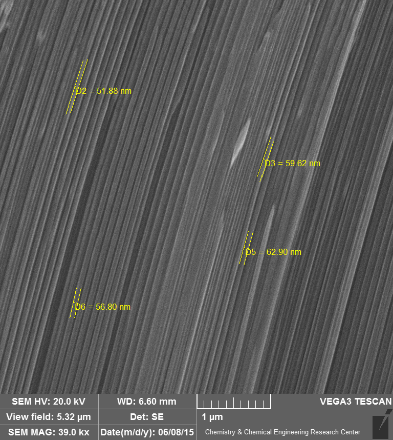
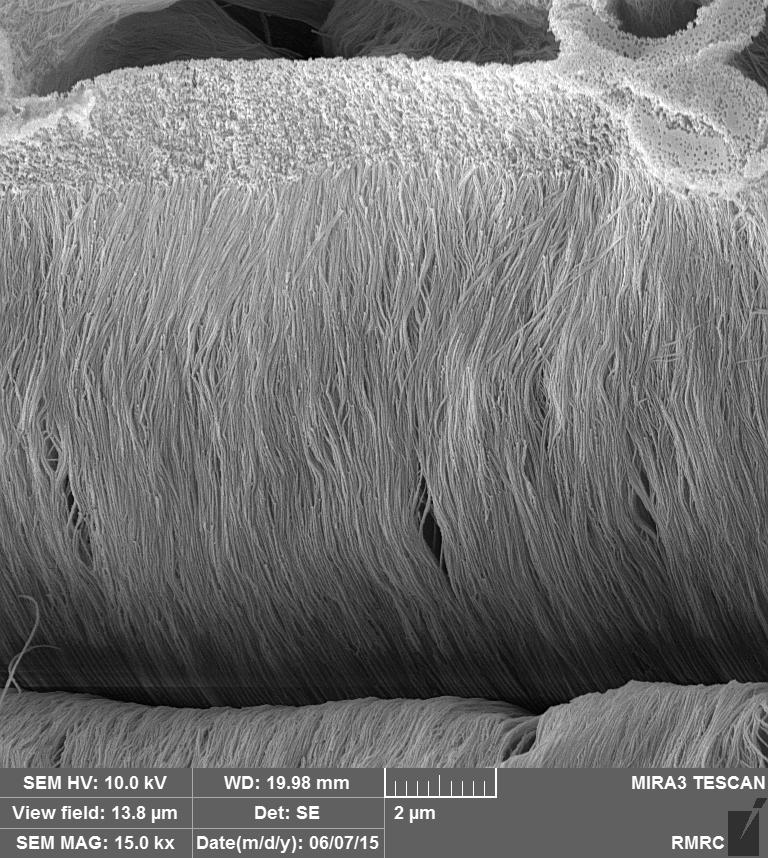
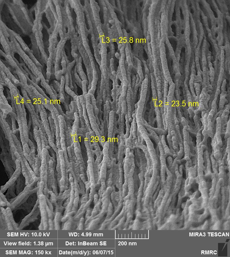
FE-SEM microscopy technique is used to investigate the morphology of Cu-Sn nanowires after dissolution of AAO template in 1M NaOH solution. In fig. 6, Cu-Sn nanowires are shown in two different resolutions, which show their long-range order structure (cref. fig. 66(a)) as well as the diameter of the nanowires (cref. fig. 66(b), 25 nm). As a result, according to fig. 66(b), it could be understood that the aspect ratio of the nanowires are increased by a factor of 2, which could increase their surface to volume ratio as well as their chemical reactivity for practical applications.
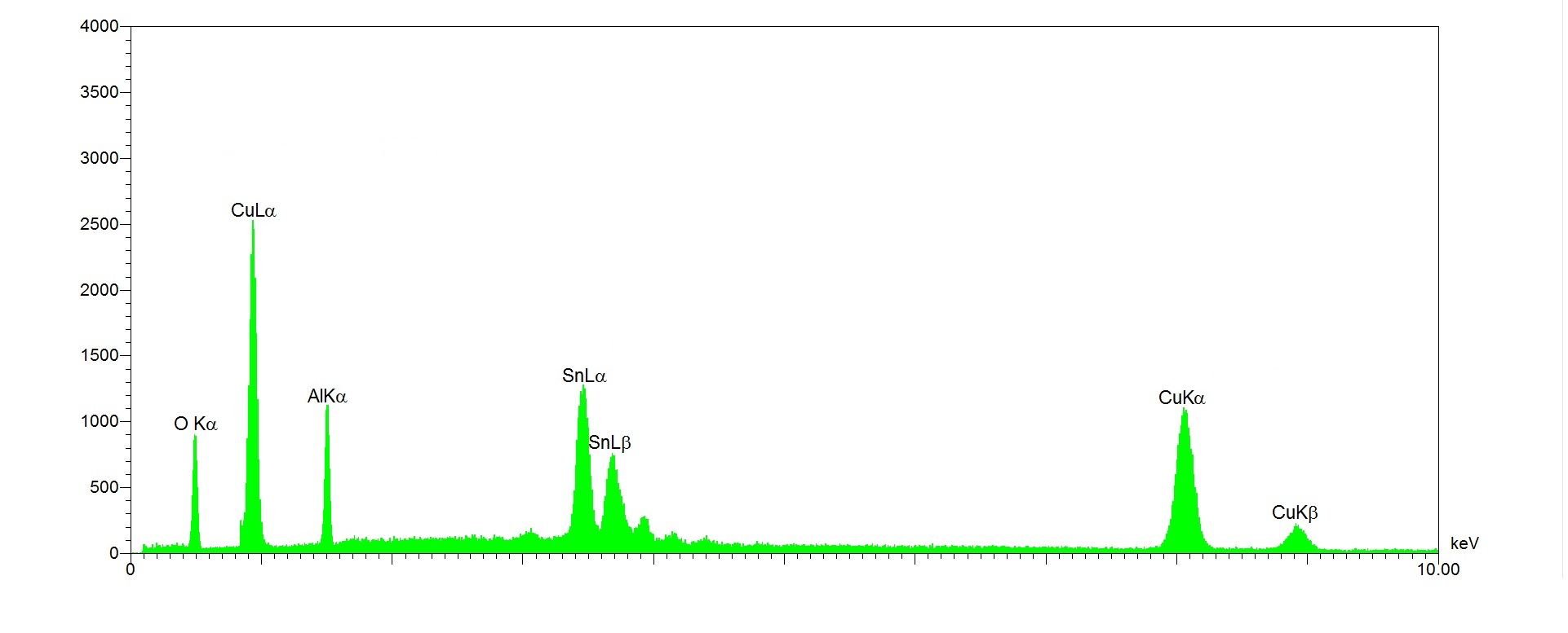
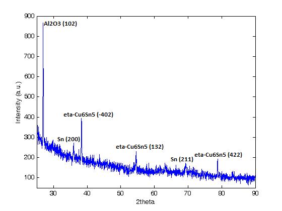
Also, the EDS and X-ray diffraction techniques are used to examine the chemical composition and crystalline structure of Cu-Sn nanowires respectively (cref. fig. 7). According to fig. 77(a), there are some residual due to presence of Aluminum and Oxygen peaks. These residual Aluminum Oxide could be eliminated by increasing the AAO template dissolution time. Additionally, due to fig. 77(b), it is shown that the cystalline structure of nanowires is a mixture of unreacted crystalline Sn and intermetallic compound. Due to conventional DC electrochemical deposition procedures, the growth of intermetallic compounds needs a post heat treatment step to facilitate the re-nucleation and growth of crystalline structures [65, 66, 67, 68, 69, 70, 71, 72, 73]. As a result, the observed intermetallic compound (, cref. fig. 77(b)) in Cu-Sn nanowires could be justified due to increasing the temperature during AC electrochemical deposition because of the high resistivity of pores’ walls. In fact, the electrical current flow chose the low resistance pathway through the barrier layer in order to reduce Copper and Tin ions, but the excess amount of electrical current flow through pore wall pathway will generate local thermal energy (. where is the thermal energy, is the electrical current density vector, and is the electrical conductivity), which causes local heat treatment of the amorphous mixture of Copper and Tin [74]. Furthermore, intermetallic compound shows promising higher efficiency in Lithium-ion batteries [75]. As a result, this AC electrochemical deposition technique could be optimized to eliminate the unreacted Sn in the nanowires by controlling the voltage, frequency, and chemical composition of the solution.
Additionally, by using EDS results, it is possible to find a direct relation between the solution chemistry and the nanowires chemical composition, which could be used to optimize this AC electrochemical deposition procedure aiming to maximize the amount of intermetallic compound and efficiency of Lithium-ion batteries. Hence, the solution and nanowires chemical compositions of 10 samples (swept concentration from 0 to 0.5M) are tabulated in table 1.
| Sample No. | Sn wt. % in solution | Sn wt. % in nanowires |
|---|---|---|
| 1 | 0 | 0 |
| 2 | 17.19 | 23.21 |
| 3 | 31.84 | 30.69 |
| 4 | 44.46 | 42.52 |
| 5 | 55.46 | 51.66 |
| 6 | 65.13 | 60.03 |
| 7 | 73.70 | 72.76 |
| 8 | 81.34 | 80.05 |
| 9 | 94.39 | 87.58 |
| 10 | 100 | 100 |
The experimental data as well as the linear fitted equation for the relation of the solution and nanowires chemical compositions are plotted in fig. 8.
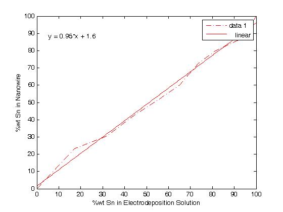
As a result, the final fitted equation which could relate the chemical composition of solution with nanowires structure, is obtained as:
| (3) |
This relation (cref. equation 3) could be used to optimize the chemical composition as well as crystalline structure of Cu-Sn nanowires and ultimately increase the efficiency of Lithium-ion batteries.
4 Conclusions
In this research, an AC electrochemical deposition technique is developed, which could be easily used to synthesize metallic nanowires with highly-ordered structure and reasonable controllability over the chemical composition as well as the crystalline structure. Additionally, this technique could facilitate the large-scale production of nanostructures due to the in-situ heat treatment of nanowires as well as the room temperature operating environment. As a result, this technique could be generalized to develop industrial scale coating facilities, which could be used in Lithium-ion battery production as well as other industries, such as: biomedical applications [76, 77, 78, 79], oil and gas extraction plants [80, 81, 82], and nanoparticles technologies [83]. Finally, these Cu-Sn nanowires’ production technique should be optimized by using the proposed electrochemical synthesizing procedure, and be examined in assembled Lithium-ion batteries to accurately measure their capacity as well as efficiency in order to achieve higher cyclability.
References
-
[1]
W. Deng, X. Wang, C. Liu, C. Li, M. Xue, R. Li, F. Pan,
Mutual independence ensured
long-term cycling stability: Template-free electrodeposited sn4ni3
nanoparticles as anode material for lithium-ion batteries, ACS Applied
Energy Materials 1 (2) (2018) 312–318.
arXiv:https://doi.org/10.1021/acsaem.7b00242, doi:10.1021/acsaem.7b00242.
URL https://doi.org/10.1021/acsaem.7b00242 -
[2]
M. Tian, W. Wang, Y. Wei, R. Yang,
Stable
high areal capacity lithium-ion battery anodes based on three-dimensional
ni–sn nanowire networks, Journal of Power Sources 211 (2012) 46 – 51.
doi:https://doi.org/10.1016/j.jpowsour.2012.03.084.
URL http://www.sciencedirect.com/science/article/pii/S0378775312007057 -
[3]
J. Ren, X. He, L. Wang, W. Pu, C. Jiang, C. Wan,
Nanometer
copper–tin alloy anode material for lithium-ion batteries, Electrochimica
Acta 52 (7) (2007) 2447 – 2452.
doi:https://doi.org/10.1016/j.electacta.2006.08.055.
URL http://www.sciencedirect.com/science/article/pii/S0013468606009339 -
[4]
Y. H. Yoon, D. S. Kim, M. Kim, M. S. Park, Y.-C. Lee, K. H. Kim, I. T. Kim,
J. Hur, S. G. Lee,
Investigation
of electrochemical performance on carbon supported tin-selenium bimetallic
anodes in lithium-ion batteries, Electrochimica Acta 266 (2018) 193 – 201.
doi:https://doi.org/10.1016/j.electacta.2017.12.188.
URL http://www.sciencedirect.com/science/article/pii/S0013468617327627 -
[5]
H.-C. Shin, M. Liu,
Three-dimensional
porous copper–tin alloy electrodes for rechargeable lithium batteries,
Advanced Functional Materials 15 (4) 582–586.
arXiv:https://onlinelibrary.wiley.com/doi/pdf/10.1002/adfm.200305165,
doi:10.1002/adfm.200305165.
URL https://onlinelibrary.wiley.com/doi/abs/10.1002/adfm.200305165 -
[6]
H. Peng, R. Li, J. Hu, W. Deng, F. Pan,
Core–shell
sn–ni–cu-alloy@carbon nanorods to array as three-dimensional anode by
nanoelectrodeposition for high-performance lithium ion batteries, ACS
Applied Materials & Interfaces 8 (19) (2016) 12221–12227, pMID: 27113033.
arXiv:https://doi.org/10.1021/acsami.6b03383, doi:10.1021/acsami.6b03383.
URL https://doi.org/10.1021/acsami.6b03383 -
[7]
S. Sengupta, A. Patra, M. Akhtar, K. Das, S. B. Majumder, S. Das,
3d
microporous sn-sb-ni alloy impregnated ni foam as high-performance negative
electrode for lithium-ion batteries, Journal of Alloys and Compounds 705
(2017) 290 – 300.
doi:https://doi.org/10.1016/j.jallcom.2017.02.125.
URL http://www.sciencedirect.com/science/article/pii/S0925838817305637 -
[8]
B. Polat, A. Abouimrane, N. Sezgin, O. Keles, K. Amine,
Use
of multilayered ni-sn and ni-sn-c thin film anodes for lithium-ion
batteries, Electrochimica Acta 135 (2014) 585 – 593.
doi:https://doi.org/10.1016/j.electacta.2014.05.024.
URL http://www.sciencedirect.com/science/article/pii/S0013468614010056 -
[9]
K. Zhuo, M.-G. Jeong, C.-H. Chung,
Highly
porous dendritic ni–sn anodes for lithium-ion batteries, Journal of Power
Sources 244 (2013) 601 – 605, 16th International Meeting on Lithium
Batteries (IMLB).
doi:https://doi.org/10.1016/j.jpowsour.2013.01.055.
URL http://www.sciencedirect.com/science/article/pii/S037877531300092X -
[10]
D. Jiang, X. Ma, Y. Fu,
High-performance sn–ni
alloy nanorod electrodes prepared by electrodeposition for lithium ion
rechargeable batteries, Journal of Applied Electrochemistry 42 (8) (2012)
555–559.
doi:10.1007/s10800-012-0434-0.
URL https://doi.org/10.1007/s10800-012-0434-0 -
[11]
T. Yamamoto, T. Nohira, R. Hagiwara, A. Fukunaga, S. Sakai, K. Nitta,
Charge–discharge
behavior of sn–ni alloy film electrodes in an intermediate temperature
ionic liquid for the electrolyte of a sodium secondary battery,
Electrochimica Acta 193 (2016) 275 – 283.
doi:https://doi.org/10.1016/j.electacta.2016.02.059.
URL http://www.sciencedirect.com/science/article/pii/S0013468616303383 -
[12]
G. Wang, B. Wang, X. Wang, J. Park, S. Dou, H. Ahn, K. Kim,
Sn/graphene nanocomposite with 3d
architecture for enhanced reversible lithium storage in lithium ion
batteries, J. Mater. Chem. 19 (2009) 8378–8384.
doi:10.1039/B914650D.
URL http://dx.doi.org/10.1039/B914650D -
[13]
H. Qin, X. Zhao, N. Jiang, Z. Li,
Solvothermal
synthesis and ex situ xrd study of nano-ni3sn2 used as an anode material for
lithium-ion batteries, Journal of Power Sources 171 (2) (2007) 948 – 952.
doi:https://doi.org/10.1016/j.jpowsour.2007.05.097.
URL http://www.sciencedirect.com/science/article/pii/S0378775307012037 -
[14]
J. Hassoun, S. Panero, B. Scrosati,
Electrodeposited
ni–sn intermetallic electrodes for advanced lithium ion batteries, Journal
of Power Sources 160 (2) (2006) 1336 – 1341, special issue including
selected papers presented at the International Workshop on Molten Carbonate
Fuel Cells and Related Science and Technology 2005 together with regular
papers.
doi:https://doi.org/10.1016/j.jpowsour.2006.02.068.
URL http://www.sciencedirect.com/science/article/pii/S0378775306003806 -
[15]
G. Ferrara, L. Damen, C. Arbizzani, R. Inguanta, S. Piazza, C. Sunseri,
M. Mastragostino,
Snco
nanowire array as negative electrode for lithium-ion batteries, Journal of
Power Sources 196 (3) (2011) 1469 – 1473.
doi:https://doi.org/10.1016/j.jpowsour.2010.09.039.
URL http://www.sciencedirect.com/science/article/pii/S0378775310016459 -
[16]
L. Huang, H.-B. Wei, F.-S. Ke, X.-Y. Fan, J.-T. Li, S.-G. Sun,
Electrodeposition
and lithium storage performance of three-dimensional porous reticular sn–ni
alloy electrodes, Electrochimica Acta 54 (10) (2009) 2693 – 2698.
doi:https://doi.org/10.1016/j.electacta.2008.11.044.
URL http://www.sciencedirect.com/science/article/pii/S0013468608013303 -
[17]
D. Deng, M. G. Kim, J. Y. Lee, J. Cho,
Green energy storage materials:
Nanostructured tio2 and sn-based anodes for lithium-ion batteries, Energy
Environ. Sci. 2 (2009) 818–837.
doi:10.1039/B823474D.
URL http://dx.doi.org/10.1039/B823474D -
[18]
J. Hassoun, S. Panero, P. Simon, P. Taberna, B. Scrosati,
High-rate,
long-life ni–sn nanostructured electrodes for lithium-ion batteries,
Advanced Materials 19 (12) 1632–1635.
arXiv:https://onlinelibrary.wiley.com/doi/pdf/10.1002/adma.200602035,
doi:10.1002/adma.200602035.
URL https://onlinelibrary.wiley.com/doi/abs/10.1002/adma.200602035 -
[19]
H. Mukaibo, T. Sumi, T. Yokoshima, T. Momma, T. Osaka,
Electrodeposited sn-ni
alloy film as a high capacity anode material for lithium-ion secondary
batteries, Electrochemical and Solid-State Letters 6 (10) (2003) A218–A220.
arXiv:http://esl.ecsdl.org/content/6/10/A218.full.pdf+html, doi:10.1149/1.1602331.
URL http://esl.ecsdl.org/content/6/10/A218.abstract -
[20]
N. Tamura, M. Fujimoto, M. Kamino, S. Fujitani,
Mechanical
stability of sn–co alloy anodes for lithium secondary batteries,
Electrochimica Acta 49 (12) (2004) 1949 – 1956.
doi:https://doi.org/10.1016/j.electacta.2003.12.024.
URL http://www.sciencedirect.com/science/article/pii/S0013468603010429 -
[21]
Z. Yang, H. Liang, X. Wang, X. Ma, T. Zhang, Y. Yang, L. Xie, D. Chen, Y. Long,
J. Chen, Y. Chang, C. Yan, X. Zhang, X. Zhang, B. Ge, Z. Ren, M. Xue,
G. Chen, Atom-thin sns2–xsex
with adjustable compositions by direct liquid exfoliation from single
crystals, ACS Nano 10 (1) (2016) 755–762, pMID: 26690902.
arXiv:https://doi.org/10.1021/acsnano.5b05823, doi:10.1021/acsnano.5b05823.
URL https://doi.org/10.1021/acsnano.5b05823 -
[22]
X. Wang, D. Chen, Z. Yang, X. Zhang, C. Wang, J. Chen, X. Zhang, M. Xue,
Novel
metal chalcogenide snsse as a high-capacity anode for sodium-ion batteries,
Advanced Materials 28 (39) 8645–8650.
arXiv:https://onlinelibrary.wiley.com/doi/pdf/10.1002/adma.201603219,
doi:10.1002/adma.201603219.
URL https://onlinelibrary.wiley.com/doi/abs/10.1002/adma.201603219 -
[23]
J. Wu, Z. Zhu, H. Zhang, H. Fu, H. Li, A. Wang, H. Zhang,
A novel si/sn composite with
entangled ribbon structure as anode materials for lithium ion battery,
Scientific Reports 6 (2016) 29356 EP –, article.
URL http://dx.doi.org/10.1038/srep29356 -
[24]
J. M. Whiteley, J. W. Kim, D. M. Piper, S.-H. Lee,
High-capacity and
highly reversible silicon-tin hybrid anode for solid-state lithium-ion
batteries, Journal of The Electrochemical Society 163 (2) (2016) A251–A254.
arXiv:http://jes.ecsdl.org/content/163/2/A251.full.pdf+html, doi:10.1149/2.0701602jes.
URL http://jes.ecsdl.org/content/163/2/A251.abstract -
[25]
D.-H. Nam, J. W. Kim, J.-H. Lee, S.-Y. Lee, H.-A.-S. Shin, S.-H. Lee, Y.-C.
Joo, Tunable sn structures in
porosity-controlled carbon nanofibers for all-solid-state lithium-ion battery
anodes, J. Mater. Chem. A 3 (2015) 11021–11030.
doi:10.1039/C5TA00884K.
URL http://dx.doi.org/10.1039/C5TA00884K -
[26]
J.-H. Cho, S. T. Picraux, Enhanced
lithium ion battery cycling of silicon nanowire anodes by template growth to
eliminate silicon underlayer islands, Nano Letters 13 (11) (2013)
5740–5747, pMID: 24144166.
arXiv:https://doi.org/10.1021/nl4036498, doi:10.1021/nl4036498.
URL https://doi.org/10.1021/nl4036498 -
[27]
H. Xiang, T. Guo, M. Xu, H. Lu, S. Liu, G. Yu,
Ultrathin copper nanowire
synthesis with tunable morphology using organic amines for transparent
conductors, ACS Applied Nano Materials 1 (8) (2018) 3754–3759.
arXiv:https://doi.org/10.1021/acsanm.8b00722, doi:10.1021/acsanm.8b00722.
URL https://doi.org/10.1021/acsanm.8b00722 -
[28]
C. Kang, S. Yang, M. Tan, C. Wei, Q. Liu, J. Fang, G. Liu,
Purification of copper
nanowires to prepare flexible transparent conductive films with high
performance, ACS Applied Nano Materials 1 (7) (2018) 3155–3163.
arXiv:https://doi.org/10.1021/acsanm.8b00326, doi:10.1021/acsanm.8b00326.
URL https://doi.org/10.1021/acsanm.8b00326 -
[29]
L. Li, H. Liu, C. Qin, Z. Liang, A. Scida, S. Yue, X. Tong, R. R. Adzic, S. S.
Wong, Ultrathin ptxsn1–x
nanowires for methanol and ethanol oxidation reactions: Tuning performance by
varying chemical composition, ACS Applied Nano Materials 1 (3) (2018)
1104–1115.
arXiv:https://doi.org/10.1021/acsanm.7b00289, doi:10.1021/acsanm.7b00289.
URL https://doi.org/10.1021/acsanm.7b00289 -
[30]
Y. Kanno, T. Suzuki, Y. Yamauchi, K. Kuroda,
Preparation of au nanowire films by
electrodeposition using mesoporous silica films as a template: Vital effect
of vertically oriented mesopores on a substrate, The Journal of Physical
Chemistry C 116 (46) (2012) 24672–24680.
arXiv:https://doi.org/10.1021/jp308772b, doi:10.1021/jp308772b.
URL https://doi.org/10.1021/jp308772b -
[31]
A. Ertan, S. N. Tewari, O. Talu,
Electrodeposition
of nickel nanowires and nanotubes using various templates, Journal of
Experimental Nanoscience 3 (4) (2008) 287–295.
arXiv:https://www.tandfonline.com/doi/pdf/10.1080/17458080802570617,
doi:10.1080/17458080802570617.
URL https://www.tandfonline.com/doi/abs/10.1080/17458080802570617 -
[32]
N. Liu, F. Wei, L. Liu, H. S. S. Lai, H. Yu, Y. Wang, G.-B. Lee, W. J. Li,
Optically-controlled
digital electrodeposition of thin-film metals for fabrication of
nano-devices, Opt. Mater. Express 5 (4) (2015) 838–848.
doi:10.1364/OME.5.000838.
URL http://www.osapublishing.org/ome/abstract.cfm?URI=ome-5-4-838 -
[33]
B. Luo, D. Yang, M. Liang, L. Zhi,
Large-scale fabrication of single
crystalline tin nanowire arrays, Nanoscale 2 (2010) 1661–1664.
doi:10.1039/C0NR00206B.
URL http://dx.doi.org/10.1039/C0NR00206B -
[34]
G. A. Gelves, Z. T. M. Murakami, M. J. Krantz, J. A. Haber,
Multigram synthesis of copper
nanowires using ac electrodeposition into porous aluminium oxide templates,
J. Mater. Chem. 16 (2006) 3075–3083.
doi:10.1039/B603442J.
URL http://dx.doi.org/10.1039/B603442J -
[35]
J. Ning, Q. Dai, T. Jiang, K. Men, D. Liu, N. Xiao, C. Li, D. Li, B. Liu,
B. Zou, G. Zou, W. W. Yu, Facile
synthesis of tin oxide nanoflowers: A potential high-capacity
lithium-ion-storage material, Langmuir 25 (3) (2009) 1818–1821, pMID:
19105789.
arXiv:https://doi.org/10.1021/la8037473, doi:10.1021/la8037473.
URL https://doi.org/10.1021/la8037473 -
[36]
G. Heidari, S. M. Mousavi Khoie, M. E. Abrishami, M. Javanbakht,
Electrodeposition of cu–sn
alloys: theoretical and experimental approaches, Journal of Materials
Science: Materials in Electronics 26 (3) (2015) 1969–1976.
doi:10.1007/s10854-014-2636-1.
URL https://doi.org/10.1007/s10854-014-2636-1 -
[37]
G. Heidari, S. M. Mousavi Khoie, M. Yousefi, M. Ghasemifard,
Kinetic model of copper
electrodeposition in sulfate solution containing trisodium citrate complexing
agent, Russian Journal of Electrochemistry 52 (5) (2016) 470–476.
doi:10.1134/S1023193516050050.
URL https://doi.org/10.1134/S1023193516050050 -
[38]
D. Borissov, S. Isik-Uppenkamp, M. Rohwerder,
Fabrication of iron nanowire arrays
by electrodeposition into porous alumina, The Journal of Physical Chemistry
C 113 (8) (2009) 3133–3138.
arXiv:https://doi.org/10.1021/jp809202h, doi:10.1021/jp809202h.
URL https://doi.org/10.1021/jp809202h -
[39]
F. Hekmat, B. Sohrabi, M. S. Rahmanifar,
Growth of the cobalt
nanowires using ac electrochemical deposition on anodized aluminum oxide
templates, Journal of Nanostructure in Chemistry 4 (2) (2014) 105.
doi:10.1007/s40097-014-0105-2.
URL https://doi.org/10.1007/s40097-014-0105-2 -
[40]
N. Ji, W. Ruan, C. Wang, Z. Lu, B. Zhao,
Fabrication of silver decorated
anodic aluminum oxide substrate and its optical properties on
surface-enhanced raman scattering and thin film interference, Langmuir
25 (19) (2009) 11869–11873, pMID: 19522476.
arXiv:https://doi.org/10.1021/la901521j, doi:10.1021/la901521j.
URL https://doi.org/10.1021/la901521j -
[41]
H. M. Gong, Z. K. Zhou, S. Xiao, X. R. Su, Q. Q. Wang,
Strong near-infrared
avalanche photoluminescence from ag nanowire arrays, Plasmonics 3 (2) (2008)
59–64.
doi:10.1007/s11468-008-9054-2.
URL https://doi.org/10.1007/s11468-008-9054-2 -
[42]
S. Gavrilov, L. Nosova, I. Sieber, A. Belaidi, L. Dloczik, T. Dittrich,
Synthesis
of semiconductor nanowires by pulsed current electrodeposition of metal with
subsequent sulfurization, physica status solidi (a) 202 (8) 1497–1501.
arXiv:https://onlinelibrary.wiley.com/doi/pdf/10.1002/pssa.200461161,
doi:10.1002/pssa.200461161.
URL https://onlinelibrary.wiley.com/doi/abs/10.1002/pssa.200461161 -
[43]
A. N. Belov, S. A. Gavrilov, V. I. Shevyakov, E. N. Redichev,
Pulsed electrodeposition of
metals into porous anodic alumina, Applied Physics A 102 (1) (2011)
219–223.
doi:10.1007/s00339-010-5907-6.
URL https://doi.org/10.1007/s00339-010-5907-6 -
[44]
S. Shamaila, R. Sharif, S. Riaz, M. Khaleeq-ur Rahman, X. F. Han,
Fabrication and magnetic
characterization of co x pt1−x nanowire arrays, Applied Physics A 92 (3)
(2008) 687–691.
doi:10.1007/s00339-008-4622-z.
URL https://doi.org/10.1007/s00339-008-4622-z -
[45]
Z. Wang, M. Brust, Fabrication
of nanostructure via self-assembly of nanowires within the aao template,
Nanoscale Research Letters 2 (1) (2006) 34.
doi:10.1007/s11671-006-9026-4.
URL https://doi.org/10.1007/s11671-006-9026-4 -
[46]
S. J. Hurst, E. K. Payne, L. Qin, C. A. Mirkin,
Multisegmented
one-dimensional nanorods prepared by hard-template synthetic methods,
Angewandte Chemie International Edition 45 (17) 2672–2692.
arXiv:https://onlinelibrary.wiley.com/doi/pdf/10.1002/anie.200504025,
doi:10.1002/anie.200504025.
URL https://onlinelibrary.wiley.com/doi/abs/10.1002/anie.200504025 -
[47]
N. Ahmad, A. Jaral, G. Bano, S. Batool, H. Dilpazir, M. Jameel, S. Khan,
J. Iqbal, A. Majid, M. M. Naseer, S. A. Shah,
Ac potential-dependent
concentration variation and domain wall pinning in co1−x zn x (x=0.4−0.5)
nanorods, Journal of Superconductivity and Novel Magnetism 29 (2) (2016)
509–513.
doi:10.1007/s10948-015-3274-4.
URL https://doi.org/10.1007/s10948-015-3274-4 -
[48]
X. Fang, L. Wu, L. Hu,
Zns
nanostructure arrays: A developing material star, Advanced Materials 23 (5)
585–598.
arXiv:https://onlinelibrary.wiley.com/doi/pdf/10.1002/adma.201003624,
doi:10.1002/adma.201003624.
URL https://onlinelibrary.wiley.com/doi/abs/10.1002/adma.201003624 -
[49]
A. I. Vorobyova, E. A. Outkina, A. A. Khodin,
Nickel/alumina
nanocomposites by ac electrochemical processing, Applied Physics A 122 (2)
(2016) 130.
doi:10.1007/s00339-016-9611-z.
URL https://doi.org/10.1007/s00339-016-9611-z -
[50]
A. M. Mebed, A. M. Abd-Elnaiem, N. M. Al-Hosiny,
Electrochemical fabrication
of 2d and 3d nickel nanowires using porous anodic alumina templates, Applied
Physics A 122 (6) (2016) 565.
doi:10.1007/s00339-016-0099-3.
URL https://doi.org/10.1007/s00339-016-0099-3 -
[51]
C. S. Lewis, L. Wang, H. Liu, J. Han, S. S. Wong,
Synthesis, characterization, and
formation mechanism of crystalline cu and ni metallic nanowires under
ambient, seedless, surfactantless conditions, Crystal Growth & Design
14 (8) (2014) 3825–3838.
arXiv:https://doi.org/10.1021/cg500324j, doi:10.1021/cg500324j.
URL https://doi.org/10.1021/cg500324j -
[52]
C. Y. Han, G. A. Willing, Z. Xiao, H. H. Wang,
Control of the anodic aluminum oxide
barrier layer opening process by wet chemical etching, Langmuir 23 (3)
(2007) 1564–1568, pMID: 17241088.
arXiv:https://doi.org/10.1021/la060190c, doi:10.1021/la060190c.
URL https://doi.org/10.1021/la060190c -
[53]
P. G. Schiavi, P. Altimari, A. Rubino, F. Pagnanelli,
Electrodeposition
of cobalt nanowires into alumina templates generated by one-step
anodization, Electrochimica Acta 259 (2018) 711 – 722.
doi:https://doi.org/10.1016/j.electacta.2017.11.035.
URL http://www.sciencedirect.com/science/article/pii/S0013468617323861 -
[54]
W. J. Stępniowski, W. Florkiewicz, M. Michalska-Domańska, M. Norek,
T. Czujko,
A
comparative study of electrochemical barrier layer thinning for anodic
aluminum oxide grown on technical purity aluminum, Journal of
Electroanalytical Chemistry 741 (2015) 80 – 86.
doi:https://doi.org/10.1016/j.jelechem.2015.01.025.
URL http://www.sciencedirect.com/science/article/pii/S1572665715000405 -
[55]
E. Gillette, S. Wittenberg, L. Graham, K. Lee, G. Rubloff, P. Banerjee, S. B.
Lee, Anodization control for
barrier-oxide thinning and 3d interconnected pores and direct
electrodeposition of nanowire networks on native aluminium substrates, Phys.
Chem. Chem. Phys. 17 (2015) 3873–3879.
doi:10.1039/C4CP04211E.
URL http://dx.doi.org/10.1039/C4CP04211E -
[56]
T. R. B. Foong, A. Sellinger, X. Hu,
Origin of the bottlenecks in
preparing anodized aluminum oxide (aao) templates on ito glass, ACS Nano
2 (11) (2008) 2250–2256.
arXiv:https://doi.org/10.1021/nn800435n, doi:10.1021/nn800435n.
URL https://doi.org/10.1021/nn800435n -
[57]
W. J. Stepniowski, M. Moneta, K. Karczewski, M. Michalska-Domanska, T. Czujko,
J. M. Mol, J. G. Buijnsters,
Fabrication
of copper nanowires via electrodeposition in anodic aluminum oxide templates
formed by combined hard anodizing and electrochemical barrier layer
thinning, Journal of Electroanalytical Chemistry 809 (2018) 59 – 66.
doi:https://doi.org/10.1016/j.jelechem.2017.12.052.
URL http://www.sciencedirect.com/science/article/pii/S157266571730927X - [58] J. Zhang, J. E. Kielbasa, D. L. Carroll, Nanostructure of the nanopores in anodic aluminum oxide films used as template to fabricate ag nanowires, Journal of Materials Research 24 (5) (2009) 1735–1740. doi:10.1557/jmr.2009.0206.
-
[59]
C. T. Rueden, J. Schindelin, M. C. Hiner, B. E. DeZonia, A. E. Walter, E. T.
Arena, K. W. Eliceiri,
Imagej2: Imagej for the next
generation of scientific image data, BMC Bioinformatics 18 (1) (2017) 529.
doi:10.1186/s12859-017-1934-z.
URL https://doi.org/10.1186/s12859-017-1934-z -
[60]
N. Tasaltin, S. Öztürk, N. Kilinç, H. Yüzer,
Z. Öztürk,
Fabrication of
vertically aligned pd nanowire array in aao template by electrodeposition
using neutral electrolyte, Nanoscale Res Lett 5 (7) (2010) 1137–1143,
1556-276X-5-1137[PII].
doi:10.1007/s11671-010-9616-z.
URL http://www.ncbi.nlm.nih.gov/pmc/articles/PMC2894036/ -
[61]
T. Gorisse, L. Dupré, P. Gentile, M. Martin, M. Zelsmann, D. Buttard,
Highly organised and dense
vertical silicon nanowire arrays grown in porous alumina template on ¡100¿
silicon wafers, Nanoscale Research Letters 8 (1) (2013) 287.
doi:10.1186/1556-276X-8-287.
URL https://doi.org/10.1186/1556-276X-8-287 -
[62]
J. Liang, H. Luo, R. Beresford, J. Xu,
A growth pathway for highly ordered
quantum dot arrays, Applied Physics Letters 85 (24) (2004) 5974–5976.
arXiv:https://doi.org/10.1063/1.1834987, doi:10.1063/1.1834987.
URL https://doi.org/10.1063/1.1834987 -
[63]
G. D. Sulka, V. Moshchalkov, G. Borghs, J.-P. Celis,
Electrochemical impedance
spectroscopic study of barrier layer thinning in nanostructured aluminium,
Journal of Applied Electrochemistry 37 (7) (2007) 789–797.
doi:10.1007/s10800-007-9312-6.
URL https://doi.org/10.1007/s10800-007-9312-6 -
[64]
L. Bouchama, N. Azzouz, N. Boukmouche, J. Chopart, A. Daltin, Y. Bouznit,
Enhancing
aluminum corrosion resistance by two-step anodizing process, Surface and
Coatings Technology 235 (2013) 676 – 684.
doi:https://doi.org/10.1016/j.surfcoat.2013.08.046.
URL http://www.sciencedirect.com/science/article/pii/S0257897213008232 - [65] D. Wang, Y. Ruan, L. Zhang, S. Zhang, P. Ma, The study on preparation of zno nanowire in aao by electrodeposition method, in: 2010 3rd International Nanoelectronics Conference (INEC), 2010, pp. 1335–1336. doi:10.1109/INEC.2010.5424866.
- [66] S. L. Cheng, Y. P. Wei, C. H. Chung, Synthesis of cobalt metal nanowire arrays and the interfacial reactions of cobalt nanowires on (001)si, in: The 4th IEEE International NanoElectronics Conference, 2011, pp. 1–2. doi:10.1109/INEC.2011.5991646.
-
[67]
F. Márquez, C. Morant, V. López, F. Zamora, T. Campo, E. Elizalde,
An alternative route for the
synthesis of silicon nanowires via porous anodic alumina masks, Nanoscale
Research Letters 6 (1) (2011) 495.
doi:10.1186/1556-276X-6-495.
URL https://doi.org/10.1186/1556-276X-6-495 - [68] C.-G. Kuo, H. Chang, J.-H. Wang, Fabrication of zno nanowires arrays by anodization and high-vacuum die casting technique, and their piezoelectric properties, Sensors 16 (4).
-
[69]
L. Yang, Y. She, W. Zhang, Y. Chen, Y. Tang, S. Zhao, A. Hu, Q. Wang, L. Wu,
Synthesis and
characterisation of γ-fe2o3 nanowire arrays via a versatile, simple and
low-cost method, Journal of Experimental Nanoscience 7 (4) (2012) 477–484.
arXiv:https://doi.org/10.1080/17458080.2010.538442, doi:10.1080/17458080.2010.538442.
URL https://doi.org/10.1080/17458080.2010.538442 -
[70]
C. Han, S. Yang, K. G. Chang, P. P. Wang, R.-i. Murakami, X. P. Song,
Structure transition and
magnetism of bcc-ni nanowires, J. Mater. Chem. C 3 (2015) 1004–1010.
doi:10.1039/C4TC02428A.
URL http://dx.doi.org/10.1039/C4TC02428A -
[71]
H.-W. Wang, H.-C. Lin, Y.-C. Yeh,
Synthesis
of fe3o4 nanowire arrays via precipitation in templates and microwave
hydrothermal process, International Journal of Applied Ceramic Technology
7 (s1) E33–E38.
arXiv:https://onlinelibrary.wiley.com/doi/pdf/10.1111/j.1744-7402.2009.02364.x,
doi:10.1111/j.1744-7402.2009.02364.x.
URL https://onlinelibrary.wiley.com/doi/abs/10.1111/j.1744-7402.2009.02364.x -
[72]
J.-B. Shi, P.-F. Wu, H.-S. Lin, Y.-T. Lin, H.-W. Lee, C.-T. Kao, W.-H. Liao,
S.-L. Young, Synthesis and
characterization of single-crystalline zinc tin oxide nanowires, Nanoscale
Research Letters 9 (1) (2014) 210.
doi:10.1186/1556-276X-9-210.
URL https://doi.org/10.1186/1556-276X-9-210 -
[73]
D. Carlier, J.-P. Ansermet,
Electrochemical
synthesis and magnetic properties of cofe2o4 nanowire arrays, Journal of The
Electrochemical Society 153 (5) (2006) C277–C281.
arXiv:http://jes.ecsdl.org/content/153/5/C277.full.pdf+html, doi:10.1149/1.2178655.
URL http://jes.ecsdl.org/content/153/5/C277.abstract - [74] Y. S. Jang, J. H. Kim, S. H. Choi, K. M. Yang, Y. C. Kang, Electrochemical properties of cu6sn5-c composite powders with mixture of cu5sn6@void@c yolk-shell, cu5sn6 alloy, and hollow carbon.
-
[75]
G. F. Ortiz, M. C. López, R. Alcántara, J. L. Tirado,
Electrodeposition
of copper–tin nanowires on ti foils for rechargeable lithium
micro-batteries with high energy density, Journal of Alloys and Compounds
585 (2014) 331 – 336.
doi:https://doi.org/10.1016/j.jallcom.2013.09.163.
URL http://www.sciencedirect.com/science/article/pii/S0925838813023372 -
[76]
A. Amirjani, M. Yousefi, M. Cheshmaroo,
Parametrical
optimization of stent design; a numerical-based approach, Computational
Materials Science 90 (2014) 210 – 220.
doi:https://doi.org/10.1016/j.commatsci.2014.04.002.
URL http://www.sciencedirect.com/science/article/pii/S092702561400233X -
[77]
N. W. Bressloff, G. Ragkousis, N. Curzen,
Design optimisation of
coronary artery stent systems, Annals of Biomedical Engineering 44 (2)
(2016) 357–367.
doi:10.1007/s10439-015-1373-9.
URL https://doi.org/10.1007/s10439-015-1373-9 -
[78]
Y.-H. Lim, H.-Y. Jeong,
Finite element analyses
for improved design of peripheral stents, Computer Methods in Biomechanics
and Biomedical Engineering 20 (6) (2017) 653–662, pMID: 28349767.
arXiv:https://doi.org/10.1080/10255842.2017.1286650, doi:10.1080/10255842.2017.1286650.
URL https://doi.org/10.1080/10255842.2017.1286650 -
[79]
M. Basiaga, W. Walke, M. Antonowicz, A. Sambok-Kiełbowicz, D. Nakonieczny,
M. Gawlikowski, B. Zawidlak-Węgrzyńska, C. Krawczyk,
Effect
of thin sio2 layers deposited by means of atomic layer deposition method on
the mechanical and physical properties of stainless steel,
Materialwissenschaft und Werkstofftechnik 49 (5) 562–567.
arXiv:https://onlinelibrary.wiley.com/doi/pdf/10.1002/mawe.201700241,
doi:10.1002/mawe.201700241.
URL https://onlinelibrary.wiley.com/doi/abs/10.1002/mawe.201700241 -
[80]
M. Yousefi, M. H. Farghadin, A. Farzadi,
Investigate
the causes of cracks in welded 310 stainless steel used in the flare tip,
Engineering Failure Analysis 53 (2015) 138 – 147.
doi:https://doi.org/10.1016/j.engfailanal.2015.04.002.
URL http://www.sciencedirect.com/science/article/pii/S1350630715001156 -
[81]
M. Ghalambaz, M. Abdollahi, A. Eslami, A. Bahrami,
A
case study on failure of aisi 347h stabilized stainless steel pipe in a
petrochemical plant, Case Studies in Engineering Failure Analysis 9 (2017)
52 – 62.
doi:https://doi.org/10.1016/j.csefa.2017.07.001.
URL http://www.sciencedirect.com/science/article/pii/S2213290217300391 -
[82]
I. Taie, A. Al-Shahrani, N. Qari, A. Fihri, W. Al-Obaid, G. Alabedi,
High
temperature corrosion resistant coatings for gas flare systems, Ceramics
International 44 (5) (2018) 5124 – 5130.
doi:https://doi.org/10.1016/j.ceramint.2017.12.114.
URL http://www.sciencedirect.com/science/article/pii/S0272884217328201 -
[83]
M. Yousefi, M. M. Khoie,
Molecular dynamics
simulation of ni/cu-ni nanoparticles sintering under various
crystallographic, thermodynamic and multi-nanoparticles conditions, The
European Physical Journal D 69 (3) (2015) 71.
doi:10.1140/epjd/e2015-50830-4.
URL https://doi.org/10.1140/epjd/e2015-50830-4