Broadband excitation spectrum of bulk crystals and thin layers of PtTe2
Abstract
We explore the broadband excitation spectrum of bulk PtTe2 using electron energy loss spectroscopy and density functional theory. In addition to infrared modes related to intraband 3D Dirac plasmon and interband transitions between the 3D Dirac bands, we observe modes at 3.9, 7.5 and 19.0 eV in the ultraviolet region. The comparison of the excitation spectrum with the calculated orbital-resolved density of states allows us to ascribe spectral features to transitions between specific electronic states. Additionally, we study the thickness dependence of the high-energy plasmon in the PtTe2 thin films. We show that, unlike graphene, the high-energy plasmon in PtTe2 thin film gets red-shifted by 2.5 eV with increasing thickness.
I Introduction
Recently, the PtX2 (X=Se, Te, S) class of transition-metal dichalcogenides (TMDCs) have attracted a huge interest of the scientific community. This class of TMDCs combines promising application capabilities along with the fundamental physics interest arising from the existence of topological type-II Dirac fermions. (Castellanos-Gomez, 2016; Li et al., 2017; Soluyanov et al., 2015; Yan et al., 2017; Bahramy et al., 2017; Noh et al., 2017; Zhang et al., 2017; Huang et al., 2016; Yan et al., 2017; Chang et al., 2017) As opposed to type-I Dirac materials, which have a closed Fermi surface with either an electron or a hole pocket, type-II Dirac materials have an unbounded Fermi surface with both electron and hole pockets. (Soluyanov et al., 2015) The presence of bulk topological Dirac node forces the existence of massless surface states. This provides massless charge carriers with ultrahigh mobility confined at the surface plane. (Bahramy et al., 2017)
Thin layers of PtX2 class of materials are equally interesting because of their air stability, high mobility, and superior gas sensing properties, among others. Li et al. (2017); Lin et. al. (2017); Zhao et al. (2017); Chia et al. (2016); Wang et. al. (2015); Wang et al. (2016) The quantum confinement effect dramatically changes the properties of the thin layers of PtTe2 which undergo a metal-semiconductor transition with decreasing thickness. (Ma et al., 2018; Ciarrocchi et al., 2018) Apart from this, the monolayer exhibits a unique property: because of local dipole-induced Rashba effect, opposite spins with the same energy gets spatially separated on the opposite sides of the monolayer. Yao et al. (2017) This is known as spin layer locking and it can have potential applications in the electrically tunable spintronic devices.
Preceding discussions made it clear that PtX2 class of materials has emerged as a promising material for the future electronics. While the band structure of PtTe2 has been explored comprehensively (Bahramy et al., 2017), along with the Dirac plasmons (collective density excitations) in the infrared range of the electromagnetic spectrum Politano et al. (2018), the high-energy excitations in PtTe2 still remain unexplored. The comprehension of the excitation spectrum of collective modes in the visible-ultraviolet is crucial to devise broadband photodetectors (Koppens et al., 2014; Yu et al., 2018), ultraviolet-imaging applications (Zhang et al., 2015) and broadband plasmonic devices. (Ou et al., 2014; Bisio et al., 2014) Monolayer PtTe2 has the smallest energy band gap in the PtX2 class of materials(Guo and Wang, 2016), offering it an advantage over the other members for applications in nano-electronics.
Motivated by this, in this paper we probe the broadband excitation spectrum of bulk crystals and thin layers of PtTe2, using electron energy loss spectroscopy (EELS) Rocca (1995) complemented by detailed ab-initio calculations. EELS probes the broadband dielectric response of the system to a negatively charged probe, allowing for spectral contributions from both plasmonic modes and non-vertical transitions from valence-band to conduction-band electronic states. Therefore, EELS investigations supplement the studies of the absorption and emission processes of TMDCs in the long-wavelength limit (Zeng and Cui, 2015) involving only vertical transitions from occupied to unoccupied states.
The nature of various experimentally probed EELS excitations is identified by means of calculations of the band-structure and the loss function based on density-functional theory (DFT). In addition to the bulk excitation spectrum, we also explore the changes in the broadband excitation spectrum of PtTe2 on reducing its thickness to few layers. Contrarily to the case of graphene and phosphorene, a blue-shift of the high-energy plasmon frequency is observed for thin layers compared to the bulk.(Eberlein et al., 2008; Wachsmuth et al., 2014; Ghosh et al., 2017)
The manuscript is organized as follows: In Sec. II we briefly describe the crystal structure, experimental details related to the growth and characterization of PtTe2 along with that of the reflection EELS. This is followed by a discussion of the theoretical ab-initio calculation of the EELS spectrum and other computational details in Sec. III. The broadband EELS spectrum of bulk PtTe2 is discussed in Sec. IV, followed by the discussion of the excitation spectrum of thin layers in Sec. V. Finally, we summarize our findings in Sec. VI.
II Growth, Crystal structure, Characterization and details of EELS
II.1 Growth
Single crystals of PtTe2 were prepared by the self-flux method. High-purity Pt (99.99 %) foil and Te ingot (99.9999 %) were mixed in the ratio of 1:17 and wrapped in a quartz tube under vacuum. The quartz tube was heated to 1000 ∘C, dwelled there for 8 hours, and slowly cooled at a rate of 3-5 ∘C/h to 500 ∘C. Successively, the excess Te flux was separated by centrifugation. The resulting crystals have typical dimensions of mm (Zhao et al., 2017) with the c-axis perpendicular to the plates and can be easily cleaved. The structure of the grown crystals was examined by X-ray diffraction (Bruker D2 PHASER) using Cu Kα radiation and Laue diffraction at room temperature.
Thin flakes of PtTe2 were obtained by liquid-phase exfoliation of bulk PtTe2 in N-methylpyrrolidone (NMP).
II.2 Crystal Structure
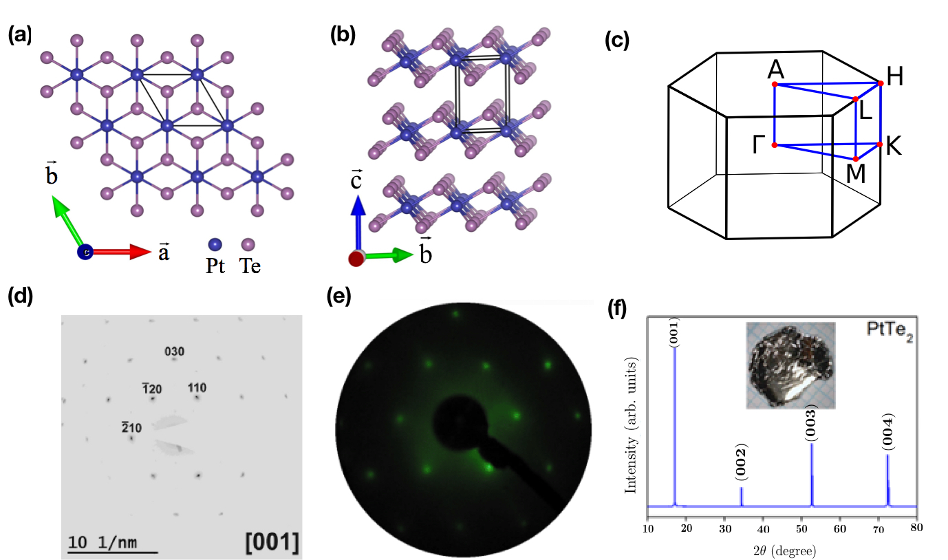
Bulk PtTe2 belongs to the large family of 1T-metal dichalcogenides with CdI2 type crystal structure [space group Pm1(164)]. The bulk structure can be viewed as a collection of isolated monolayers stacked in the out of plane direction – see Fig. 1(a) and 1(b). In each of these monolayers there are three sublayers, Te-Pt-Te, where the central Pt atom is strongly bonded with six neighbouring Te atoms forming a hexagonal honeycomb structure. Both selected area electron diffraction (SAED) and low-energy electron diffraction (LEED) patterns shown in Fig. 1(d) and 1(e) match with [0001]-oriented flakes and bulk PtTe2, respectively. Correspondingly, the XRD pattern only exhibits (00n) peaks as shown in Fig. 1(f).
II.3 Characterization
To demonstrate cleanliness, the surface has been characterized by means of vibrational spectroscopy and X-ray photoelectron spectroscopy, without finding any contamination (see appendix B, and C). Once prepared in ultra-high vacuum, the surface remains uncontaminated for a timescale of several weeks, thus ensuring sample stability. The low-energy electron diffraction (LEED) pattern shows sharp spots against a low background – see Fig. 1(e).
II.4 Electron Energy Loss Spectroscopy
The reflection EELS experiments were performed at room temperature by means of an EELS apparatus with two 50 mm hemispherical deflectors for both monochromator and analyzers, mounted in an ultra-high vacuum chamber at the University of Calabria, Italy. The primary electron beam impinges on the sample with an incident angle of 43∘ with respect to the surface normal, along the direction of the surface Brillouin zone. The primary electron beam energy is eV.
SAED and STEM-EELS analyses were carried out at room temperature on a FEI Tecnai G2 F20 TWIN TEM, equipped with a Gatan Enfinium SE spectrometer at Istituto Italiano di Tecnologia, Genoa (Italy). For these experiments a primary electron beam energy keV and a collection angle of 13 mrad were used. Samples for TEM analyses were prepared by drop casting of the flakes dispersion onto a holey carbon-coated Cu grid. The EELS spectra were collected from flakes regions suspended on holes in the carbon support film.
III Theory
III.1 Energy Loss function
The theoretical calculation of the electron energy loss function starts with the non-interacting density-density response function for a periodic lattice. It is obtained using the Adler-Wiser formula given byAdler (1962); Wiser (1963),
| (1) | |||
The wave function , eigenvalue , and the corresponding Fermi-Dirac occupation function at wave vector for the band with index are obtained from the ground-state calculations performed using DFT.
The interacting density-density response function can be obtained within the framework of time-dependent DFT (TDDFT) by solving a Dyson-like equation. Using a plane-wave basis for a periodic system, for a given , it can be expressed as
where and are the reciprocal lattice vector and the Bloch wave vector, respectively, and is the interaction kernel, including both the Coulomb or Hartree term, as well as the exchange correlations.
Using the calculated matrix, the dielectric matrix, , can obtained as,
| (2) |
The macroscopic dielectric constant can be obtained from the dielectric matrix via the equation,
| (3) |
The dynamical loss function, which is directly related to the experimental excitation spectrum probed by EELS, is now obtained from the macroscopic dielectric function,
| (4) |
Plasmons (collective density excitations) are characterized by the zeroes of the real part of the macroscopic dielectric function (the denominator of the density-density response function within RPA). Thus, they appear as peaks in the EELS spectrum. The calculations of the loss function are performed using the generalized RPA, which uses the local-field factors to add the impact of the exchange and correlation effects, in addition to the Hartree field Giuliani and Vignale (2005).
III.2 Computational details
Electronic band structure calculations were performed using a plane-wave basis set within the framework of DFT, as implemented in the VASP package.(Kohn and Sham, 1965; Kresse and Furthmüller, 1996) We use the PAW pseudopotentials with 500 eV kinetic energy cut-off for the plane-wave basis set.(Kresse and Joubert, 1999) The exchange-correlation part of the potential has been treated within the framework of generalized approximation scheme developed by Perdew-Burke-Ernzerhof.(Perdew et al., 1996) Starting from the experimental structure, we relax all the atomic positions until the forces on each atom are less than 0.001 eV/Å. Spin-orbit interaction has been considered as a perturbation and treated in a self-consistent manner.
In order to calculate the response functions we use the GPAW code, which employs a real-space representation of the PAW potentials. Mortensen et al. (2005); Enkovaara et. al. (2010); Bahn and Jacobsen (2002) A kinetic energy cutoff of 500 eV has been used for the plane-wave basis set. We use a 12212220 -grid to calculate the momentum dependence of the loss function. To incorporate the local-field effects, we use a plane-wave cutoff of 60 eV which corresponds to 85 plane waves. A broadening parameter eV is assumed in all calculations of the response function.
IV Broadband spectrum of bulk
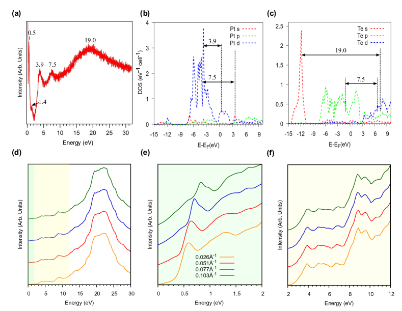
The experimental broadband EELS spectra of PtTe2 bulk sample, measured with an electron beam energy of 100 eV, is shown in Fig. 2(a). The broadband EELS spectrum shows distinctly resolved peaks at energies , , , and eV, among others. The lowest energy peak at 0.5 eV is the intra-band gapped 3D Dirac plasmon excitation in bulk PtTe2, which disperses with the momentum [see Fig. 2(e)]. It has been discussed in detail in Ref. [Politano et al., 2018]. Here, we will focus on the remaining inter-band excitations, which are relatively less dispersive compared to the intra-band 3D Dirac plasmon peak. We find that their peak location and relative intensity is nearly independent on scattering geometry and, consequently on the momentum in a momentum range of of 0.0-0.2 Å-1.
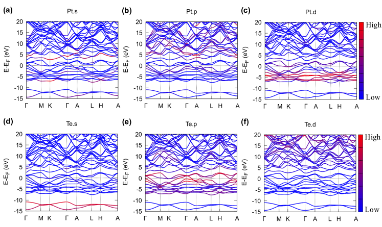
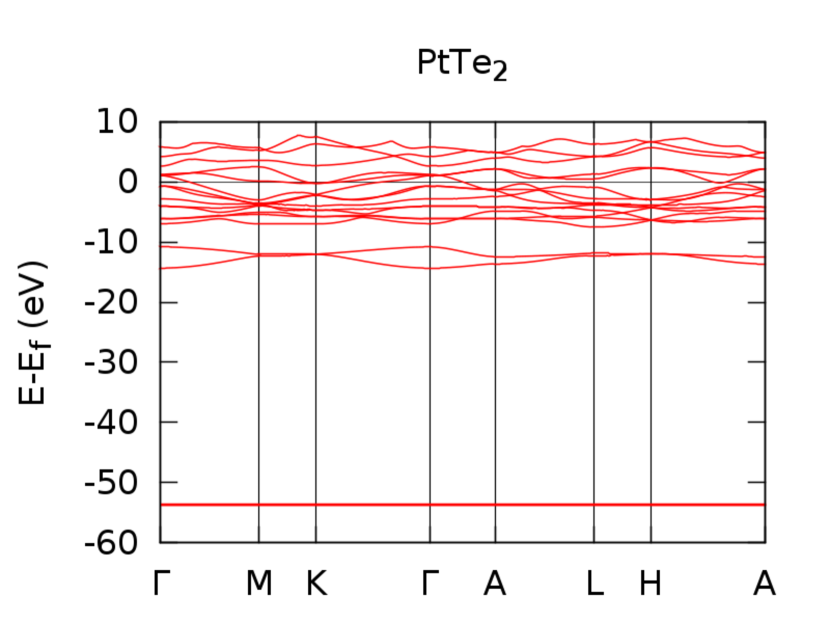
In order to identify the inter-band transitions corresponding to the observed peaks in the EELS spectrum, we show the orbital-resolved density of states (DOS) in Fig. 2(b)-(c). The corresponding orbital-resolved band structure plot is shown in Fig. 3. The energetically lower valence band (VB) is situated approximately between -15 and -10 eV and it is mostly dominated by Te5s states. The upper VB extends from -7 eV up to the Fermi level and mostly comprises of Pt5d and Te5p orbitals. The lower conduction-band states till 3 eV are also primarily formed by Pt5d and Te5p orbitals. The conduction-band states at higher energy have contributions mainly from the Pt6p and Te5d orbitals. Comparison of the orbital-resolved DOS with the observed spectral features in the broadband EELS spectrum allows us to identify the prominent states involved in the transitions. We find that the peaks at 3.9, 7.5 and 19.0 eV are predominantly connected to Pt Pt5d; Te Te5d; and Te Te5d transitions, respectively, as marked by arrows in Fig. 2(b)-(c). The theoretical loss function in Fig. 2(d)-(f) also captures the qualitative features of the experimental excitation spectrum reasonably well.
It is worth reminding that EELS peaks cannot precisely match the energies of single-particle transitions observed with optical spectroscopies, as maxima in the loss function are related to the maxima in . Conversely, optical transitions are identified with maxima in ] (Wooten, 1972), that are actually shifted with respect to the maxima of (Liebsch, 2013). Having discussed the EELS spectrum of the bulk PtTe2 crystal, we now proceed to discuss the EELS spectrum of thin PtTe2 layers in the next section.
V Broadband spectrum of thin layers
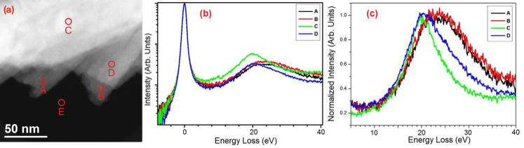
In this section, we explore the thickness dependence of the broadband EELS spectrum of PtTe2 thin films. To this aim, we have employed the STEM-EELS technique, which affords the spatial resolution necessary to identify regions with different thickness within the flakes. As shown in Fig. 4(a), the liquid-phase exfoliation of PtTe2 has produced flakes with inhomogeneous thickness. Therefore, for STEM-EELS experiments different thicknesses were probed on different areas of same fragments.
Previously, the thickness dependence of the high energy EELS peaks has been done for the case of plasmons of graphene. In graphene, the plasmon energy shifts by about 10 eV when going from monolayer graphene to multilayers. (Lu et al., 2009; Eberlein et al., 2008; Wachsmuth et al., 2014) Remarkably, a similar blue-shift has been detected by both reflection EELS in graphene layers epitaxially grown on silicon carbide (Lu et al., 2009), and by EELS-TEM in free-standing graphene flakes exfoliated from graphite. (Eberlein et al., 2008; Wachsmuth et al., 2014) This is irrespective of the dissimilarities in the plasmon energy in the monolayer regime (10 eV in the latter case(Eberlein et al., 2008; Wachsmuth et al., 2014) and 14.6 eV in the former one(Lu et al., 2009)). This blue-shift of the plasmon energy in graphene with increasing thickness had been ascribed to the effect of interlayer Coulomb coupling Wachsmuth et al. (2014). In contrast to graphene, the high energy plasmon peak in phosphorene does not show any thickness dependence Wu et al. (2015).
Our STEM-EELS investigation suggests that in PtTe2 the plasmon band changes in both line-shape and energy position as a function of thickness. Specifically, a symmetrical line-shape, centered at about 23 eV (Fig. 4c), is recorded for thinner flakes, whereas an asymmetrical line-shape, with a corresponding centroid around 20.5 eV, are revealed for thicker flakes. Thus, in contrast to grapheneEberlein et al. (2008); Wachsmuth et al. (2014), and phosphoreneWu et al. (2015) the high energy plasmon peak in PtTe2 is red-shifted with increasing thickness. However, the layer-dependent plasmon-energy shift in PtTe2 is much lower (2.5 eV) than that of graphene (10 eV). The change in the line shape, with an asymmetric shape characterizing the thinner regions, is ascribable to the multiple contributions (i.e., due to regions with different thickness) to the spectra acquired in the thinner regions of the flakes. The presence of contributions from regions few nm away from the position of the electron beam is due to the delocalization of inelastic scattering, prominent in the low energy-loss range Ahn (2004); Egerton (1996).
VI Conclusions
We have probed the broadband excitation spectrum of bulk crystals and thin layers of PtTe2, using EELS in reflection mode for bulk and STEM-EELS for thin layers. In the case of bulk PtTe2 we find different modes in the ultraviolet regime at 3.9, 7.5 and 19.0 eV, in addition to the excitations associated to the 3D Dirac cones observed in the infrared range at 0.5 and 1.4 eV. These observations are well explained by the DFT-based orbital-resolved band-structure and DOS calculations. Specifically, we find that in bulk PtTe2 the observed peaks at 3.9, 7.5 and 19.0 eV are predominantly connected to Pt Pt5d; Te Te5d; and Te Te5d transitions, respectively. In thin layers, with decreasing thickness, the high-energy plasmon peak gets shifted from 20.5 to 23.0 eV. This red-shift with increasing thickness is in contrast to the blue-shift observed in case of graphene. Moreover, with increasing number of layers an increase in the anisotropy of the line-shape of the high-energy plasmon peak is observed. This peculiarity can be exploited for characterizing the thickness of PtTe2 thin films. Similar physics is expected to play out in other members of the family, including PdTe2 and PtSe2, among others.
Appendix A Valence-band states in PtTe2
As an additional check we explicitly check that there are no valence-band states below the -14 eV in PtTe2, by calculating the band-structure over a wide energy range. The calculated band-structure is shown in Fig. 5: it is evident that there are no valence-band states in PtTe2 from approximately -14 to - 50 eV.
Appendix B Surface chemical reactivity of PtTe2 single crystals
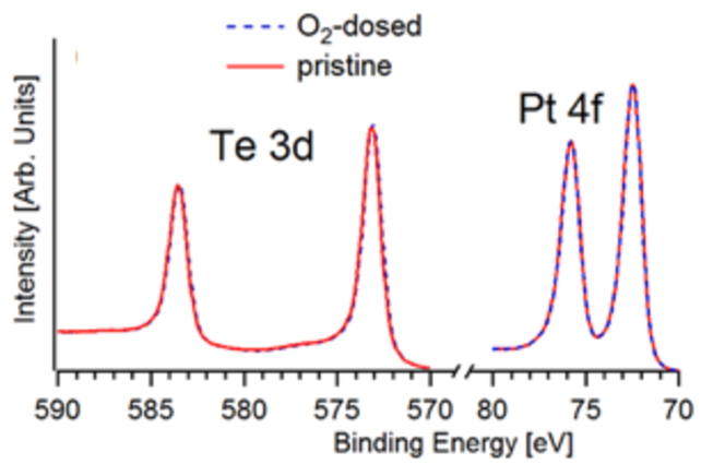
To evaluate the surface chemical reactivity of PtTe2, we have carried out high-resolution X-ray photoelectron spectroscopy (XPS) experiments (Fig. 6). We addressed firstly the evolution of Pt 4f and Te 3d core levels upon several treatments (O2 dosage and air exposure), with respect to spectra measured for pristine PtTe2. From the analysis of Te 3d core-level spectra (Fig. 6), we deduce that the as-cleaved undefected PtTe2 surface is inert to oxygen exposure. In fact, only 3d5/2 and 3d3/2 core levels at the binding energies of 573.1 and 583.5 eV, corresponding to an oxidation state Te(0), are observed in Fig. 6 for both the pristine PtTe2 (red curve) and the same surface exposed to a dose of 106 L (1 L= mbar s) of O2 at room temperature (dashed blue curve).
The Pt 4f doublet reported in Fig. 6 is observed at binding energies of 72.5 (4f7/2) and 75.9 (4f5/2) eV, respectively. Similar values of the binding energy for Pt-4f core levels have been reported for PtSe2 Yim et al. (2016); Wang et al. (2016).
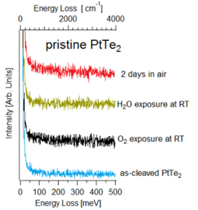
To further assess the surface chemical reactivity in PtTe2-based systems, we have also carried out vibrational experiments by means of high-resolution electron energy loss spectroscopy (HREELS). Explicitly, we have exposed pristine PtTe2 to water and oxygen. The corresponding vibrational spectra are reported in Fig. 7. For the case of pristine (undefected) PtTe2, the vibrational spectrum remains featureless even after exposure of water and oxygen at room temperature (Fig. 7). Likewise, no vibrational peaks are revealed in the air-exposed undefected PtTe2 surface (red curve in Fig. 7). Combined with the XPS results reported in Fig. 6, these data lead to the conclusion that undefected PtTe2 does not react at room temperature with ambient gases. This finding has a particular interest in view of applications in optoelectronics based on PtTe2.
References
- Castellanos-Gomez (2016) Andres Castellanos-Gomez, “Why all the fuss about 2d semiconductors?” Nature Photonics 10, 202 (2016).
- Li et al. (2017) Liang Li, Weike Wang, Yang Chai, Huiqiao Li, Mingliang Tian, and Tianyou Zhai, “Few layered phototransistor on h bn with high gain,” Advanced Functional Materials 27, 1701011 (2017).
- Soluyanov et al. (2015) Alexey A. Soluyanov, Dominik Gresch, Zhijun Wang, QuanSheng Wu, Matthias Troyer, Xi Dai, and B. Andrei Bernevig, “Type-ii weyl semimetals,” Nature 527, 495 EP – (2015).
- Yan et al. (2017) Mingzhe Yan, Huaqing Huang, Kenan Zhang, Eryin Wang, Wei Yao, Ke Deng, Guoliang Wan, Hongyun Zhang, Masashi Arita, Haitao Yang, Zhe Sun, Hong Yao, Yang Wu, Shoushan Fan, Wenhui Duan, and Shuyun Zhou, “Lorentz-violating type-ii dirac fermions in transition metal dichalcogenide ptte2,” Nature Communications 8, 257 (2017).
- Bahramy et al. (2017) M. S. Bahramy, O. J. Clark, B.-J. Yang, J. Feng, L. Bawden, J. M. Riley, I. Markovic, F. Mazzola, V. Sunko, D. Biswas, S. P. Cooil, M. Jorge, J. W. Wells, M. Leandersson, T. Balasubramanian, J. Fujii, I. Vobornik, J. E. Rault, T. K. Kim, M. Hoesch, K. Okawa, M. Asakawa, T. Sasagawa, T. Eknapakul, W. Meevasana, and P. D. C. King, “Ubiquitous formation of bulk dirac cones and topological surface states from a single orbital manifold in transition-metal dichalcogenides,” Nature Materials 17, 21 (2017).
- Noh et al. (2017) Han-Jin Noh, Jinwon Jeong, En-Jin Cho, Kyoo Kim, B. I. Min, and Byeong-Gyu Park, “Experimental realization of type-ii dirac fermions in a superconductor,” Phys. Rev. Lett. 119, 016401 (2017).
- Zhang et al. (2017) Kenan Zhang, Mingzhe Yan, Haoxiong Zhang, Huaqing Huang, Masashi Arita, Zhe Sun, Wenhui Duan, Yang Wu, and Shuyun Zhou, “Experimental evidence for type-ii dirac semimetal in ,” Phys. Rev. B 96, 125102 (2017).
- Huang et al. (2016) Huaqing Huang, Shuyun Zhou, and Wenhui Duan, “Type-ii dirac fermions in the class of transition metal dichalcogenides,” Phys. Rev. B 94, 121117 (2016).
- Chang et al. (2017) Tay-Rong Chang, Su-Yang Xu, Daniel S. Sanchez, Wei-Feng Tsai, Shin-Ming Huang, Guoqing Chang, Chuang-Han Hsu, Guang Bian, Ilya Belopolski, Zhi-Ming Yu, Shengyuan A. Yang, Titus Neupert, Horng-Tay Jeng, Hsin Lin, and M. Zahid Hasan, “Type-ii symmetry-protected topological dirac semimetals,” Phys. Rev. Lett. 119, 026404 (2017).
- Lin et. al. (2017) X. Lin et. al., “Intrinsically patterned two-dimensional materials for selective adsorption of molecules and nanoclusters,” Nat Mater 16, 717–721 (2017).
- Zhao et al. (2017) Yuda Zhao, Jingsi Qiao, Zhihao Yu, Peng Yu, Kang Xu, Shu Ping Lau, Wu Zhou, Zheng Liu, Xinran Wang, Wei Ji, and Yang Chai, “High-electron-mobility and air-stable 2d layered ptse2 fets,” Advanced Materials 29, 1604230 (2017).
- Chia et al. (2016) Xinyi Chia, Ambrosi Adriano, Petr Lazar, Zdeněk Sofer, Jan Luxa, and Martin Pumera, “Layered platinum dichalcogenides (pts2, ptse2, and ptte2) electrocatalysis: Monotonic dependence on the chalcogen size,” Advanced Functional Materials 26, 1505402 (2016).
- Wang et. al. (2015) Y Wang et. al., “Monolayer ptse2, a new semiconducting transition-metal-dichalcogenide, epitaxially grown by direct selenization of pt,” Nano Letters 15, 4013–4018 (2015).
- Wang et al. (2016) Zegao Wang, Qiang Li, Flemming Besenbacher, and Mingdong Dong, “Facile synthesis of single crystal ptse2 nanosheets for nanoscale electronics,” Advanced Materials 28, 10224–10229 (2016).
- Ma et al. (2018) Huifang Ma, Peng Chen, Bo Li, Jia Li, Ruoqi Ai, Zhengwei Zhang, Guangzhuang Sun, Kangkang Yao, Zhaoyang Lin, Bei Zhao, Ruixia Wu, Xuwan Tang, Xidong Duan, and Xiangfeng Duan, “Thickness-tunable synthesis of ultrathin type-ii dirac semimetal ptte2 single crystals and their thickness-dependent electronic properties,” Nano Letters 18, 3523–3529 (2018).
- Ciarrocchi et al. (2018) Alberto Ciarrocchi, Ahmet Avsar, Dmitry Ovchinnikov, and Andras Kis, “Thickness-modulated metal-to-semiconductor transformation in a transition metal dichalcogenide,” Nature Communications 9, 919 (2018).
- Yao et al. (2017) Wei Yao, Eryin Wang, Huaqing Huang, Ke Deng, Mingzhe Yan, Kenan Zhang, Koji Miyamoto, Taichi Okuda, Linfei Li, Yeliang Wang, Hongjun Gao, Chaoxing Liu, Wenhui Duan, and Shuyun Zhou, “Direct observation of spin-layer locking by local rashba effect in monolayer semiconducting ptse2 film,” Nature Communications 8, 14216 (2017).
- Politano et al. (2018) Antonio Politano, Gennaro Chiarello, Barun Ghosh, Krishanu Sadhukhan, Chia-Nung Kuo, Chin Shan Lue, Vittorio Pellegrini, and Amit Agarwal, “3d dirac plasmons in the type-ii dirac semimetal ,” Phys. Rev. Lett. 121, 086804 (2018).
- Koppens et al. (2014) F. H. L. Koppens, T. Mueller, Ph Avouris, A. C. Ferrari, M. S. Vitiello, and M. Polini, “Photodetectors based on graphene, other two-dimensional materials and hybrid systems,” Nature Nanotechnology 9, 780 (2014).
- Yu et al. (2018) Xuechao Yu, Peng Yu, Di Wu, Bahadur Singh, Qingsheng Zeng, Hsin Lin, Wu Zhou, Junhao Lin, Kazu Suenaga, Zheng Liu, and Qi Jie Wang, “Atomically?thin noble metal dichalcogenide: a broadband mid-infrared semiconductor,” Nature Communications 9, 1545 (2018).
- Zhang et al. (2015) X. Zhang, K. Wang, J. Ma, Q. Zhang, P. Yan, and X. Tian, “Ultraviolet imaging based on surface plasmon resonance with azo-polymer sensing layer,” IEEE Photonics Technology Letters 27, 1297–1300 (2015).
- Ou et al. (2014) Jun-Yu Ou, Jin-Kyu So, Giorgio Adamo, Azat Sulaev, Lan Wang, and Nikolay I. Zheludev, “Ultraviolet and visible range plasmonics in the topological insulator bi1.5sb0.5te1.8se1.2,” Nature Communications 5, 5139 (2014).
- Bisio et al. (2014) Francesco Bisio, Remo Proietti Zaccaria, Riccardo Moroni, Giulia Maidecchi, Alessandro Alabastri, Grazia Gonella, Angelo Giglia, Laura Andolfi, Stefano Nannarone, Lorenzo Mattera, and Maurizio Canepa, “Pushing the high-energy limit of plasmonics,” ACS Nano 8, 9239–9247 (2014).
- Guo and Wang (2016) San-Dong Guo and Jian-Li Wang, “Spin–orbital coupling effect on the power factor in semiconducting transition-metal dichalcogenide monolayers,” Semiconductor Science and Technology 31, 095011 (2016).
- Rocca (1995) M. Rocca, “Low-energy eels investigation of surface electronic excitations on metals,” Surface Science Reports 22, 1 – 71 (1995).
- Zeng and Cui (2015) Hualing Zeng and Xiaodong Cui, “An optical spectroscopic study on two-dimensional group-vi transition metal dichalcogenides,” Chem. Soc. Rev. 44, 2629–2642 (2015).
- Eberlein et al. (2008) T. Eberlein, U. Bangert, R. R. Nair, R. Jones, M. Gass, A. L. Bleloch, K. S. Novoselov, A. Geim, and P. R. Briddon, “Plasmon spectroscopy of free-standing graphene films,” Phys. Rev. B 77, 233406 (2008).
- Wachsmuth et al. (2014) P. Wachsmuth, R. Hambach, G. Benner, and U. Kaiser, “Plasmon bands in multilayer graphene,” Phys. Rev. B 90, 235434 (2014).
- Ghosh et al. (2017) Barun Ghosh, Piyush Kumar, Anmol Thakur, Yogesh Singh Chauhan, Somnath Bhowmick, and Amit Agarwal, “Anisotropic plasmons, excitons, and electron energy loss spectroscopy of phosphorene,” Phys. Rev. B 96, 035422 (2017).
- Adler (1962) Stephen L. Adler, “Quantum theory of the dielectric constant in real solids,” Phys. Rev. 126, 413–420 (1962).
- Wiser (1963) Nathan Wiser, “Dielectric constant with local field effects included,” Phys. Rev. 129, 62–69 (1963).
- Giuliani and Vignale (2005) G. Giuliani and G. Vignale, Quantum Theory of the Electron Liquid, Masters Series in Physics and Astronomy (Cambridge University Press, 2005).
- Kohn and Sham (1965) W. Kohn and L. J. Sham, “Self-consistent equations including exchange and correlation effects,” Phys. Rev. 140, A1133–A1138 (1965).
- Kresse and Furthmüller (1996) G. Kresse and J. Furthmüller, “Efficient iterative schemes for ab initio total-energy calculations using a plane-wave basis set,” Phys. Rev. B 54, 11169–11186 (1996).
- Kresse and Joubert (1999) G. Kresse and D. Joubert, “From ultrasoft pseudopotentials to the projector augmented-wave method,” Phys. Rev. B 59, 1758–1775 (1999).
- Perdew et al. (1996) John P. Perdew, Kieron Burke, and Matthias Ernzerhof, “Generalized gradient approximation made simple,” Phys. Rev. Lett. 77, 3865–3868 (1996).
- Mortensen et al. (2005) J. J. Mortensen, L. B. Hansen, and K. W. Jacobsen, “Real-space grid implementation of the projector augmented wave method,” Phys. Rev. B 71, 035109 (2005).
- Enkovaara et. al. (2010) J. Enkovaara et. al., “Electronic structure calculations with gpaw: a real-space implementation of the projector augmented-wave method,” Journal of Physics: Condensed Matter 22, 253202 (2010).
- Bahn and Jacobsen (2002) S. R. Bahn and K. W. Jacobsen, “An object-oriented scripting interface to a legacy electronic structure code,” Comput. Sci. Eng. 4, 56–66 (2002).
- Wooten (1972) Frederick Wooten, Optical Properties of Solids, (1972), 10.1016/B978-0-12-763450-0.50001-5.
- Liebsch (2013) Ansgar Liebsch, Electronic excitations at metal surfaces (Springer Science & Business Media, 2013).
- Lu et al. (2009) Jiong Lu, Kian Ping Loh, Han Huang, Wei Chen, and Andrew T. S. Wee, “Plasmon dispersion on epitaxial graphene studied using high-resolution electron energy-loss spectroscopy,” Phys. Rev. B 80, 113410 (2009).
- Wu et al. (2015) Ryan J. Wu, Mehmet Topsakal, Tony Low, Matthew C. Robbins, Nazila Haratipour, Jong Seok Jeong, Renata M. Wentzcovitch, Steven J. Koester, and K. Andre Mkhoyan, “Atomic and electronic structure of exfoliated black phosphorus,” Journal of Vacuum Science & Technology A 33, 060604 (2015).
- Ahn (2004) C.C. Ahn, Transmission electron energy loss spectrometry in materials science and the EELS atlas (Wiley-VCH, 2004).
- Egerton (1996) R.F. Egerton, Electron Energy-Loss Spectroscopy in the Electron Microscope, Language of science (Plenum Press, 1996).
- Yim et al. (2016) Chanyoung Yim, Kangho Lee, Niall McEvoy, Maria O’Brien, Sarah Riazimehr, Nina C. Berner, Conor P. Cullen, Jani Kotakoski, Jannik C. Meyer, Max C. Lemme, and Georg S. Duesberg, “High-performance hybrid electronic devices from layered ptse2 films grown at low temperature,” ACS Nano 10, 9550–9558 (2016).