Dialkali-Metal Monochalcogenide Semiconductors with High Mobility and Tunable Magnetism
Abstract
The discovery of archetypal two-dimensional (2D) materials provides enormous opportunities in both fundamental breakthroughs and device applications, as evident by the research booming in graphene, atomically thin transition-metal chalcogenides, and few-layer black phosphorous in the past decade. Here, we report a new, large family of semiconducting dialkali-metal monochalcogenides (DMMCs) with an inherent A2X monolayer structure, in which two alkali sub-monolayers form hexagonal close packing and sandwich the triangular chalcogen atomic plane. Such unique lattice structure leads to extraordinary physical properties, such as good dynamical and thermal stability, visible to near-infrared light energy gap, high electron mobility (e.g. cm2V-1S-1 in K2O). Most strikingly, DMMC monolayers (MLs) host extended van Hove singularities near the valence band (VB) edge, which can be readily accessed by moderate hole doping of cm-2. Once the critical points are reached, DMMC MLs undergo spontaneous ferromagnetic transition when the top VBs become fully spin-polarized by strong exchange interactions. Such gate tunable magnetism in DMMC MLs are promising for exploring novel device concepts in spintronics, electronics and optoelectronics.
I Introduction
Although the critical importance of dimensionality in determining the extraordinary physical properties of low-dimension systems has long been recognized since Richard Feyman, the groundbreaking experiments on graphene Novoselov et al. (2004, 2005); Zhang et al. (2005) provide a fascinating platform for exploring exotic phenomena in a rather simple hexagonal lattice. After the gold rush of graphene, the search of new two-dimensional (2D) systems have received unparalleled attention in the hope of novel physical properties and prototype functionalities. However, despite the flourishing of 2D materials Zhu et al. (2015); Vogt et al. (2012); Liu et al. (2011); Lu et al. (2016); Lee et al. (2013); Khazaei et al. (2013); Bhimanapati et al. (2015), the majority of 2D researches remain heavily focusing on the archetypal systems of graphene Geim and Grigorieva (2013), transition-metal dichalcogenides (TMDCs) Mak et al. (2010); Radisavljevic et al. (2011); Zheng et al. (2015); Wang et al. (2018a), and few-layer black phosphorus (BP) Li et al. (2014, 2016). These 2D paradigms share the common features of weak interlayer coupling by van der Waals interactions, good thermal stability at room temperature, and high charge carrier mobility. Nevertheless, very recently, there are emergent 2D materials with tempting physical properties beyond the aforementioned systems, such as the InSe family Cao et al. (2015); Banhurin et al. (2017), 2D ferromagnetic van der Waals crystals Gong et al. (2017); Huang et al. (2017), binary maingroup compounds with the BP-type puckering lattice Gomes and Carvalho (2015); Wu and Zeng (2016); Wang et al. (2018b), and the huge family of carbide and nitride based transition metal MXenes, in which M represents transition metal cation and X is C or N anion, respectively Lee et al. (2013); Naguib et al. (2012).
Here, by using ab initio density functional calculations, we discover a large family of dialkali-metal monochalcogenides (DMMCs) with excellent dynamical and thermal stability, visible to near-infrared light energy gap, and very high electron mobility of exceeding . With the same lattice structure of 1T-TMDCs, DMMCs have the inherent layer-by-layer structure with very weak interlayer coupling, due to the intrinsic +1 oxidation state of alkali cations. All these features make DMMCs a unique choice beyond TMDCs for fundamental studies of 2D systems and for developing potential electronic and optoelectronic devices. Most fascinatingly, all DMMC monolayers (MLs) host extended singularity points in the density of states near the Mexican-hat shaped valence band maximum (VBM). Using hole doping in the range of cm-2 via electrostatic or liquid ion gating, spontaneous ferromagnetic transitions, which lead to half-metallic character with full spin polarized top valence bands, can be triggered by strong exchange interactions in these 2D systems. Such gate tunable magnetism and half metallicity in DMMC MLs may pave new routes in novel device concepts for spintronics.
II Results and Discussion
II.1 Structure and Stability
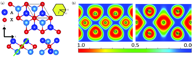
Dialkali-metal monochalcogenides form a large family with sixteen compounds in the general formula of A2X, where A represents an alkali atom (Na, K, Rb or Cs) and X is a chalcogen anion of O, S, Se or Te. The synthesis of bulk dicesium monoxide (Cs2O) was first reported in 1955 Tsai et al. (1956) with the space group (No. 166), which has the same lattice structures as the well-known 1T-TMDCs Wilson et al. (2001) as displayed in Fig. 1a and 2a. By taking van der Waals (vdW) corrections into account, the optimized lattice constants of bulk Cs2O are Å, Å, and Å, respectively, which are in excellent agreement with the experimental values Tsai et al. (1956). In the 2D limit, the monolayer of DMMCs has the space group (No. 164). The primitive unit cell consists of two alkali cations and one group-VIa anions, making A2X stoichiometry. The metal-chalcogen ratio in DMMC MLs is distinct from the well-known TMDC MLs, in which the unit cell includes two chalcogenide anions and one metal cation. For instance, in Cs2O ML, the centering O atom is surrounded by six Cs cations, forming a distinctive O-Cs octahedron, as shown in Fig. 1a. Such lattice structure is rooted in strong intralayer O-Cs ionic bonding, as revealed by the analysis of electron localization functions (ELFs). As shown in Fig. 1b, the electron densities are highly localized around Cs and O atoms with negligible inter-atom distribution, reflecting ionic bonding and electron donation from Cs to O atoms. The calculated oxidation state of O anions, as represented by the Hirshfeld charge, is nearly identical to that of BaO, also confirming the dianionic character of oxygen in Cs2O. No accumulation of electron density is observed between Cs atoms, suggesting no chemical bond between them. The A-X octahedral geometry centring the chalcogen dianion is general observed for the whole family, as presented in Fig. 1b for Na2O ML and in Supplementary Information (SI) Figure S1-S4 for the other 14 DMMC MLs.
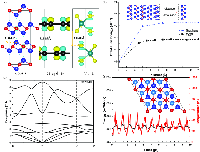
Due to the intrinsic full oxidation state (+1) of Cs, the interlayer coupling between Cs sub-MLs is very weak, which only introduces marginal changes to the in-plane lattice constants. The optimized and of Cs2O ML (4.26 Å) are almost the same as the experimental bulk value. Comparing with the paradigmatic 2D systems of MoS2 and graphite, we find that there are even less interlayer electron density localization in Cs2O as a result of dominant in-plane ionic bonding, which also means micromechanical exfoliation of Cs2O crystals can be readily achieved (Fig. 2a). Indeed, we calculate the exfoliation energy of Cs2O ML to be J/m2 (Fig. 2b), which is surprisingly lower than the value of 0.33 J/m2 for graphene Zacharia et al. (2004). It has to been emphasized here that the lower exfoliation energy of bulk Cs2O, compared with MoS2 ( 0.42 J/m2) and graphite, is consistently obtained by different vdW correction methods, which is summarized in SI Table S1.
To assess the dynamical stability, which is also crucial for the micro-exfoliation of Cs2O ML, we have computed the phonon dispersion with the finite displacement method. As shown in Fig. 2c, the good stability of ML Cs2O is evident by the positive values of all phonon modes. We further check the room-temperature (RT) thermal stability of Cs2O ML by first-principle molecular dynamics simulations. The fluctuation of energy and temperature as a function of time are plotted in Fig. 2d. After running 4000 steps (10 ps), the 331 trigonal lattice is well sustained, and the free energy of the supercell converges. Excellent dynamical and thermal stability have also been validated for the other DMMC MLs (See SI Figure S5 and S6). Thus, it is feasible to experimentally exfoliate DMMC MLs for device fabrications and applications.
II.2 Electronic Properties
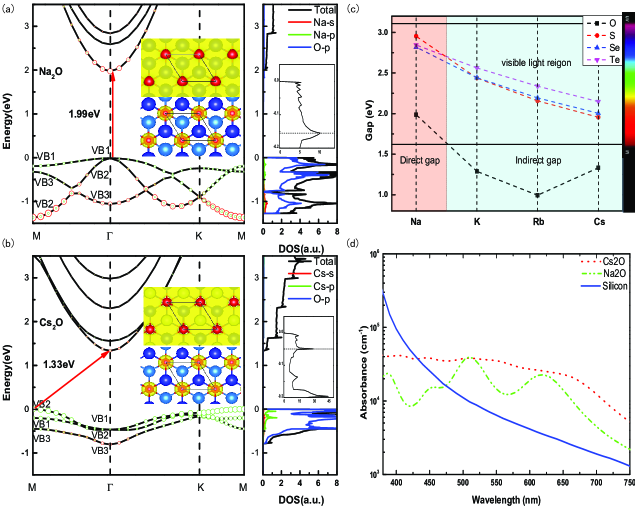
We now elucidate the electronic structures and fundamental physical properties of DMMC MLs using two representative examples of Cs2O and Na2O MLs. As shown in Fig. 3a, Na2O ML is a 2D semiconductor with a direct bandgap of 1.99 eV at the point. Noticeably, the VBM of Na2O ML is mainly contributed by O-2 orbitals (its projection weight is not shown in the energy dispersion for clarity) hybridized with very low weight of Na-2 (weighted by green triangles), while the CBM is dominated by Na-3 (red squares). The electronic band structure undergoes a pronounced change when Na is replaced by Cs, whose strongly delocalized 5 orbitals induce significant density of states (DOS) away from the point, which is still dominated by O-2. As the energy of Cs-5 orbitals is eV higher than the 2 orbitals of O, the inter -orbital hybridization reverses the energy levels of VB1 and VB2 along the direction. The resulting Cs2O ML is an indirect semiconductor with multiple VBMs centering the points (Fig. 3b). In general, for heavier cations of K, Rb and Cs, the inter -orbital hybridization with chalcogen anions is prevailing, shifting VBMs from to the point. As a result, except for Na2X (X=O, S, Se and Te), all DMMC MLs are indirect semiconductors. The inter -orbital hybridization induced direct to indirect bandgap transition from Na2X to other A2X MLs has also been confirmed by the PBE method, as shown in SI Table S2 and SI Figure S7.
As summarized in Fig. 3c, the energy gaps of DMMC MLs range from 1 eV to 3 eV, covering the near-infrared (K2O, Rb2O and Cs2O MLs) and visible light regions, which are highly desirable for optoelectronic device applications. To evaluate the optical performance, the absorption coefficients of Cs2O and Na2O MLs are directly compared with bulk silicon Green and Keevers (1995). As shown in Fig. 3d, Na2O ML shows absorption attenuation above nm, in consistent with the direct bandgap of 1.99 eV. Strikingly, indirect-bandgap Cs2O ML exhibits unrivaled cyan-to-red light absorption efficiency, which is nearly constant over the whole visible light wavelengths. Such unusual findings not only predict Cs2O MLs to be extraordinary optoelectronic materials, but also are rooted in the enormous, non-differentiable DOS in the vicinity of VBM, i.e. van Hove singularity. As shown in Fig. 3a and 3b, the top VBs of DMMC MLs, dominated by the localized orbitals of chalcogen anions, are distinctive by very flat dispersion in the momentum space. The inter -orbital hybridization in Cs2O ML drastically reduces the VB energy dispersion, which effectively enhances DOS near the VBM and creates multiple saddle points in the vicinity of , and . This leads to a prominent extended van Hove singularity in the density of states Gofron et al. (1994). It is also noteworthy that the inter -orbital hybridization also greatly enhances DOS near the CBM, which contributes significantly to the extraordinary light absorption characteristics of Cs2O ML.
Charge carrier mobility is another critical parameter for the device performance of 2D material-based devices. As summarized in Table 1 as well as in SI Table S3 and S4, the mobility of DMMC MLs are largely asymmetric between electrons and holes due to the drastic difference in the energy dispersion between the CBs and VBs, producing highly asymmetric effective mass. Noticeably, K2O ML has the highest electron mobility of 1.87 cm2V-1S-1 along the direction. Such electron mobility is comparable to the hole mobility of few-layer BP Qiao et al. (2014); Li et al. (2016) and order of magnitude larger than that of MoS2 atomic layers Radisavljevic et al. (2011). Large electron mobility in DMMC MLs may hold a great promise for applications in high-performance electronics.
We have noticed that with the same trigonal structure (, No.166), monolayer Tl2O is predicted to be a semiconductor with a direct bandgap and highly anisotropic charge carrier mobilities up to Ma et al. (2017). This is not surprising since Tl is one of the pseudo-alkali metals, in close resemblance to K both in the oxidation state and ionic radius.
II.3 Tunable Magnetism by Hole doping.
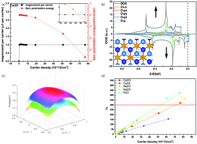
The aforementioned van Hove singularities in the top VB of DMMC MLs are associated with inherent electronic instability, when hole doping pushes the Fermi level approaching the divergent point. Taking Cs2O as an example, we find that the system undergoes a spontaneous ferromagnetic phase transition with a moderate hole doping of cm-2. In Fig. 4a, we plot the magnetic moment and the spin polarization energy per doped hole carrier as a function of . The latter represents the energy difference between the non-spin-polarized phase and the ferromagnetic phase. Clearly, the top VB becomes fully spin polarized by the critical hole doping, as manifested by the constant magnetic moment of 1 per carrier above cm-2. The spin polarization energy, which becomes -3.11 meV per carrier for a minimal hoel doping, monotonically decreases as a function of , approving that the doping-induced ferromagnetic ordering is energy favourable.
Such spontaneous ferromagnetic ordering can be well understood by the Stoner model, which has been adopted to explain the so-called “ ferromagnetism” in hole doped nitrides and oxides Peng et al. (2009). In this picture, ferromagnetism can spontaneously appear when the Stoner criterion 1 is satisfied, where is the exchange interaction strength and is the DOS at the Fermi energy of non-magnetic state. In such condition, the energy gain by exchange interactions exceeds the loss in kinetic energy, and hence the system would favor a ferromagnetic ground state. We have confirmed that the of Cs2O is always larger than one above the critical doping level, indicating that the huge DOS associated with the van Hove singularity plays a key role in the occurrence of ferromagnetism.
In Fig. 4b and 4c, we plot the spin-polarized DOS of Cs2O with a doping level of cm-2. Compared with the undoped case (Fig. 3b), the corresponding spin splitting process causes a significant energy shit of 0.1 eV between the spin-up and spin-down bands, leaving the Fermi level cutting through only one spin channel. Such half-metal state allows fully spin-polarized transport, which is crucial for spintronics applications. It is fascinating that this half-metallic ferromagnetism can be reversibly switched on and off in a 1 nm thick atomic layer without extrinsic dopant and defects.
We have found that except for Na2Te, the ferromagnetic transition can be triggered in all DMMC MLs by hole doping, ranging from cm-2 for Cs2O to cm-2 for Na2Se (see SI Figure S8-S11). The special case of Na2Te can be understood by insufficient DOS near the VBM, which is dominated by the 5 orbitals of Te. Due to much lower electron negativity, the 5 orbitals of Te are more delocalized than the other chalcogen elements. Consequently, the high dispersion of Te-5 reduce DOS near the VBM of Na2Te (SI Fig. S8), invalidating the Stoner criterion. We further evaluated the doping dependent Curie temperature () of DMMC MLs using the Heisenberg model. As shown in Fig. 4d, using cm-2 as a reference, which can be readily induced by ionic liquid gating or lithium glass gating Li et al. (2014); Lei et al. (2016), RT ferromagnetism is achievable in K2O and Na2O MLs (SI Figure S12). For Cs2O, the corresponding is K, which is nearly five times higher than the recently reported ferromagnetic CrI3 and Cr2Ge2Te6 Gong et al. (2017); Huang et al. (2017).
III Conclusions
In summary, we have reported a new family of 1T-TMDC structured dialkali-metal monochalcogenides (DMMCs), which show fascinating physical properties and great device application promises in the 2D limit. Distinctively, DMMC MLs are characterized by large electron mobility, e.g. cm2V-1S-1 for K2O and cm2V-1S-1 for Na2O, and by very flat VBs with rather weak energy dispersion. The latter are responsible for the formation of extended van Hove singularities with extremely high DOS just below the VB edge of DMMC MLs. By introducing moderate hole doping, these DMMC MLs are subjected to strong electronic instabilities induced by electron-electron interaction, which ultimately leads to spontaneous ferromagnetic phase transitions where the top VBs becomes fully spin-polarized. Using heavy doping methods of ion liquid and solid gating, we can readily increase the and switch on and off the magnetism of DMMC MLs even at room temperature.
Although alkali compounds are not very stable in air by reacting with ambient moisture, the excellent dynamical and thermal stability allows DMMC MLs to be exfoliated and encapsulated in glove box environment, which is now routine research facilities for studying air-sensitive 2D materials Li et al. (2014, 2016); Banhurin et al. (2017); Gong et al. (2017); Huang et al. (2017). It is also feasible to grow DMMC MLs by molecular beam epitaxy or by chemical vapor deposition, with abundant options of single crystal substrates of 1T- or 2H-TMDCs. By forming heterostructure with high electron affinity main-group MDCs, such as SnSe2, DMMC MLs may become effectively hole doped by interfacial charge transferring Wang et al. (2018b), which would provide the opportunity for in-situ studying the gate-tunable ferromagnetism in DMMC MLs by scanning probe microscope.
| Effective mass (m0) | mhx | mhy | mex | mey |
|---|---|---|---|---|
| Cs2O | 5.36 | 4.71 | 0.63 | 0.84 |
| Cs2S | 1.02 | 2.13 | 0.67 | 0.89 |
| Cs2Se | 0.95 | 1.99 | 0.61 | 0.81 |
| Cs2Te | 1.03 | 1.88 | 0.58 | 0.77 |
| K2O | 1.84 | 11.2 | 0.90 | 0.67 |
| Mobility (cm2V-1S-1) | ||||
| Cs2O | ||||
| Cs2S | ||||
| Cs2Se | ||||
| Cs2Te | ||||
| K2O |
References
- Novoselov et al. (2004) K. S. Novoselov, A. K. Geim, S. V. Morozov, D. Jiang, Y. Zhang, S. V. Dubonos, I. V. Grigorieva, and A. A. Firsov, “Electric field effect in atomically thin carbon films,” Science 306, 666–669 (2004).
- Novoselov et al. (2005) K. S. Novoselov, A. K. Geim, S. V. Morozov, D. Jiang, M. I. Katsnelson, I. V. Grigorieva, S. V. Dubonos, and A. A. Firsov, “Two-dimensional gas of massless Dirac fermions in graphene,” Nature 438, 197–200 (2005).
- Zhang et al. (2005) Y. B. Zhang, Y. W. Tan, H. L. Stormer, and P. Kim, “Experimental observation of the quantum Hall effect and Berry’s phase in graphene,” Nature 438, 201–204 (2005).
- Zhu et al. (2015) F. Zhu, W. Chen, Y. Xu, C. Gao, D. Guan, , C. Liu, D. Qian, S. C. Zhang, and J. F. Jia, “Epitaxial growth of two-dimensional stanene,” Nature Mater. 14, 1020–1025 (2015).
- Vogt et al. (2012) P. Vogt, P. De Padova, C. Quaresima, J. Avila, E. Frantzeskakis, , M. C. Asensio, A. Resta, B. Ealet, and G. Le Lay, “Silicene: Compelling experimental evidence for graphenelike two-dimensional silicon,” Phys. Rev. Lett. 108, 155501 (2012).
- Liu et al. (2011) C. C. Liu, W. X. Feng, and Y. G. Yao, “Quantum spin Hall effect in silicene and two-dimensional germanium,” Phys. Rev. Lett. 107, 076802 (2011).
- Lu et al. (2016) Y. H. Lu, D. Zhou, G. Q. Chang, S. Guan, W. G. Chen, Y. Z. Jiang, J. Z. Jiang, X. S. Wang, SY. A Yang, Y. P. Feng, Y. dKawazoe, and H. Lin, “Multiple unpinned Dirac points in group-Va single-layers with phosphorene structure,” Npj. Comput. Mater. 2, 16011 (2016).
- Lee et al. (2013) K. Lee, S. W. Kim, Y. Toda, S. Matsuishi, and H. Hosono, “Dicalcium nitride as a two-dimensional electride with an anionic electron layer,” Nature 494, 336–340 (2013).
- Khazaei et al. (2013) M. Khazaei, M. Arai, T. Sasaki, C. Chung, N. S. Venkataramanan, M. Estili, Y. Sakka, and Y. Kawazoe, “Novel electronic and magnetic properties of two‐dimensional transition metal carbides and nitrides,” Adv. Funct. Mater. 23, 2185–2192 (2013).
- Bhimanapati et al. (2015) G. R. Bhimanapati, Z. Lin, V. Meunier, Y. Jung, J. Cha, S. Das, D. Xiao, Y. Son, M. S. Strano, V. R. Cooper, L. Liang, S. G. Louie, W. Ringe, E. andZhou, S. S. Kim, R. R. Naik, B. G. Sumpter, H. Terrones, F. Xia, Y. Wang, J. Zhu, D. Akinwande, N. Alem, J. A. Schuller, R. E. Schaak, M. Terrones, and J. A. Robinson, “Recent advances in two-dimensional materials beyond graphene,” ACS Nano 9, 11509–11539 (2015).
- Geim and Grigorieva (2013) A. K. Geim and I. V. Grigorieva, “Van der Waals heterostructures,” Nature 499, 419–425 (2013).
- Mak et al. (2010) K. F. Mak, C. Lee, J. Hone, J. Shan, and T. F. Heinz, “Atomically thin MoS2: A new direct-gap semiconductor,” Phys. Rev. Lett. 105, 136805 (2010).
- Radisavljevic et al. (2011) B. Radisavljevic, A. Radenovic, J. Brivio, V. Giacometti, and A. Kis, “Single-layer MoS2 transistors,” Nature Nanotech. 6, 147–150 (2011).
- Zheng et al. (2015) Y. Zheng, J. Chen, M. F. Ng, H. Xu, Y. P. Liu, A. Li, S. J. O’Shea, T. Dumitrică, and K. P. Loh, “Quantum mechanical rippling of a MoS2 monolayer controlled by interlayer bilayer coupling,” Phys. Rev. Lett. 114, 065501 (2015).
- Wang et al. (2018a) G. Wang, A. Chernikov, M. M. Glazov, T. F. Heinz, X. Marie, T. Amand, and B. Urbaszek, “Colloquium: Excitons in atomically thin transition metal dichalcogenides,” Rev. Mod. Phys. 90, 021001 (2018a).
- Li et al. (2014) L. Li, Y. Yu, G. J. Ye, Q. Ge, X. Ou, H. Wu, D. Feng, X. H. Chen, and Y. B. Zhang, “Black phosphorus field-effect transistors,” Nature Nanotech. 9, 372–377 (2014).
- Li et al. (2016) L. K. Li, F. Y. Yang, G. J. Ye, Z. C. Zhang, Z. W. Zhu, W. K. Lou, X. Y. Zhou, L. Li, K. Watanabe, T. Taniguchi, K. Chang, Y. Y. Wang, X. H. Chen, and Y. B. Zhang, “Quantum Hall effect in black phosphorus two-dimensional electron system,” Nature Nanotech. 11, 592–596 (2016).
- Cao et al. (2015) T. Cao, Z. Li, and S. G. Louie, “Tunable magnetism and half-metallicity in hole-doped monolayer GaSe,” Phys. Rev. Lett. 114, 236602 (2015).
- Banhurin et al. (2017) D. A. Banhurin, A. V. Tyurnina, G. L. Yu, A. Mishchenko, V. Zolyomi, Sergey V. Morozov, R. K. Kumar, R. V. Gorbachev, Z. R. Kudrynskyi, S. Pezzini, Z. D. Kovalyuk, U. Zeitler, K. S. Novoselov, A. Patanè, L. Eaves, I. V. Grigorieva, V. I. Fal’ko, A. K. Geim, and Y. Cao, “High electron mobility, quantum Hall effect and anomalous optical response in atomically thin InSe,” Nature Nanotech. 12, 223–227 (2017).
- Gong et al. (2017) C. Gong, L. Li, Z. Li, H. Ji, A. Stern, Y. Xia, T. Cao, W. Bao, C. Wang, Y. Wang, Z. Q. Qiu, R. J. Cava, S. G. Louie, J. Xia, and X. Zhang, “Discovery of intrinsic ferromagnetism in two-dimensional van der Waals crystals,” Nature 546, 265–269 (2017).
- Huang et al. (2017) B. Huang, G. Clark, E. Navarro-Moratalla, D. R. Klein, R. Cheng, K. L. Seyler, D. Zhong, E. Schmidgall, M. A. McGuire, D. H. Cobden, W. Yao, D. Xiao, P. Jarillo-Herrero, and X. Xu, “Layer-dependent ferromagnetism in a van der Waals crystal down to the monolayer limit,” Nature 546, 270–273 (2017).
- Gomes and Carvalho (2015) L. C. Gomes and A. Carvalho, “Phosphorene analogues: Isoelectronic two-dimensional group-IV monochalcogenides with orthorhombic structure,” Phys. Rev. B 92, 085406 (2015).
- Wu and Zeng (2016) M. Wu and X. C. Zeng, “Intrinsic ferroelasticity and/or multiferroicity in two-dimensional phosphorene and phosphorene analogues,” Nano Lett. 16, 3236–3241 (2016).
- Wang et al. (2018b) Z. Wang, C. Fan, Z. X. Shen, C. Hua, Q. Hu, F. Sheng, Y. H. Lu, H. Fang, Z. Qiu, J. Lu, Z. Liu, W. Liu, Y. Huang, Z. A. Xu, D. W. Shen, and Y. Zheng, “Defects controlled hole doping and multivalley transport in SnSe single crystals,” Nature Commun. 9, 47 (2018b).
- Naguib et al. (2012) M. Naguib, O. Mashtalir, J. Carle, V. Presser, J. Lu, L. Hultman, Y. Gogotsi, and M. W. Barsoum, “Two-dimensional transition metal carbides,” ACS Nano 6, 1322–1331 (2012).
- Tsai et al. (1956) K. Tsai, P. M. Harris, and E. N. Lassettre, “The crystal structure of cesium monoxide,” J. Phys. Chem. 60, 338–344 (1956).
- Wilson et al. (2001) J. A. Wilson, F. J. Di Salvo, and S. Mahajan, “Charge-density waves and superlattices in the metallic layered transition metal dichalcogenides,” Adv. Phys. 50, 1171–1248 (2001).
- Zacharia et al. (2004) R. Zacharia, H. Ulbricht, and T. Hertel, “Interlayer cohesive energy of graphite from thermal desorption of polyaromatic hydrocarbons,” Phys. Rev. B 69, 155406 (2004).
- Green and Keevers (1995) M. A. Green and M. J. Keevers, “Optical properties of intrinsic silicon at 300 K,” Prog. Photovolt: Res. Appl. 3, 189–192 (1995).
- Gofron et al. (1994) K. Gofron, J. C. Campuzano, A. A. Abrikosov, M. Lindroos, A. Bansil, H. Ding, D. Koelling, and B. Dabrowski, “Observation of an ”extended” van Hove singularity in YBa2Cu4O8 by ultrahigh energy resolution angle-resolved photoemission,” Phys. Rev. Lett. 73, 3302 (1994).
- Qiao et al. (2014) J. Qiao, X. Kong, Z. Hu, F. Yang, and W. Ji, “High-mobility transport anisotropy and linear dichroism in few-layer black phosphorus,” Nature Commun. 5, 4475 (2014).
- Ma et al. (2017) Y. D. Ma, A. Kuc, and T. Heine, “Single-layer Tl2O: A metal-shrouded 2D semiconductor with high electronic mobility,” J. Am. Chem. Soc. 139, 11694–11697 (2017).
- Peng et al. (2009) H. Peng, H. J. Xiang, S. H. Wei, S. S. Li, J. B. Xia, and J. B. Li, “Origin and enhancement of hole-induced ferromagnetism in first-row semiconductors,” Phys. Rev. Lett. 102, 017201 (2009).
- Lei et al. (2016) B. Lei, J. H. Cui, Z. J. Xiang, C. Shang, N. Z. Wang, G. J. Ye, X. G. Luo, T. Wu, Z. Sun, and X. H. Chen, “Evolution of high-temperature superconductivity from a low- phase tuned by carrier concentration in FeSe thin flakes,” Phys. Rev. Lett. 116, 077002 (2016).
Acknowledgements.
This work is supported by the National Key R&D Program of the MOST of China (Grant Nos. 2016YFA0300204 and 2017YFA0303002), and the National Science Foundation of China (Grant Nos. 11574264 and 61574123). Y.Z. acknowledges the funding support from the Fundamental Research Funds for the Central Universities and the Thousand Talents Plan.Competing financial interests:
The authors declare no competing financial interests.