Characteristics of fast timing MCP-PMTs in magnetic fields
Abstract
The motivation of this paper is to explore the parameters that affect the performance of Microchannel Plate Photomultiplier Tubes (MCP-PMTs) in magnetic fields with the goal to guide their design to achieve a high magnetic field tolerance. MCP-PMTs based on two different designs were tested. The magnetic field tolerance of MCP-PMT based on a design providing independently biased voltages showed a significant improvement (up to 0.7 T) compared to the one utilizing an internal resistor chain design (up to 0.1 T), indicating the importance of individually adjustable voltages. The effects of the rotation angle of the MCP-PMT relative to the magnetic field direction and of the bias voltage between the photocathode and the top MCP were extensively investigated using the MCP-PMT based on the independently biased voltage design. It was found that the signal amplitude of the MCP-PMT exhibits an enhanced performance at a tilt angle of 8∘, due to the 8∘ bias angle of the MCP pores. The maximum signal amplitude was observed at different bias voltages depending on the magnetic field strength.
Keywords: Fast timing, Microchannel plate, Photodetector, Electron-Ion Collider, Particle identification detector, Magnetic field.
1 Introduction
The Electron-Ion Collider (EIC) [1], which is recommended in the 2015 Long Range Plan for Nuclear Science [2] as the highest priority for a new facility construction in the US, aims to revolutionize our understanding both of nucleon and nuclear structure and of nuclear dynamics in the many-body regime, where strongly coupled relativistic quantum fluctuations and non-perturbative effects combine to give a dynamical origin to nuclear mass and spin. The broad physics program of the EIC requires a large multipurpose spectrometer able to measure a plethora of physics processes over a wide range of energies and solid angles. Particular to the EIC is the requirement of particle indentification, i.e., the separation of electrons, pions, kaons, and protons (e//K/p) in the final state in processes such as semi-inclusive deep inelastic scattering and charm production.
To address the broad physics potential of the EIC, several detector concepts are being proposed, including the BeAST [3] and the sPHENIX [4] concepts from Brookhaven National Laboratory (BNL), the JLEIC full acceptance detector [5] from Thomas Jefferson National Accelerator Facility (JLab), and the TOPSiDE 5D particle flow detector [6] from Argonne National Laboratory (ANL). These detector concepts feature different layouts of sub-systems, which have been worked out to varying detail. Common to all concepts are the use of Time-Of-Flight (TOF) systems and imaging Cherenkov detectors for hadron particle identification. Integration of these sub-systems into the central detector requires to placing their photo-sensors in the non-uniform fringe field of the solenoidal magnet. Thus particle identification at the EIC requires low-cost photon sensors with picosecond timing resolution, millimeter spatial resolution, high rate capability, and last but not least high radiation and magnetic field tolerance.
The microchannel plate photomultiplier tube (MCP-PMT) [7] is a compact photosensor consisting of a photocathode for photon-electron conversion, two MCPs in a stacked chevron configuration for electron amplification and a readout system for charge collection. The compact design and confined electron amplification by secondary electron emission inside the micron size MCP pores provide the MCP-PMT with picosecond timing resolution and millimeter position resolution, ideal for application in time-of-flight systems and imaging Cherenkov detectors. The LAPPD collaboration [8] between universities, U.S. national laboratories, and industrial partners developed the technology to manufacture the world’s largest MCP based photosensor, the Large-Area Picosecond Photon Detector (LAPPDTM). A critical aspect of the LAPPDTM technology is its use of low-cost, very large area (20 20 cm2) MCPs [9] within an all glass vacuum envelope. The MCPs used in LAPPDsTM are made from bundled and fused capillaries of borosilicate glass functionalized through atomic-layer deposition [10, 11, 12] of conductive and secondary-electron emissive material layers. This revolutionary process eliminates the chemical etching and hydrogen firing steps employed in traditional MCP manufacturing, which caused the glass to become brittle and resulted in strong ion feedback. These features and the inherent mechanical stability of borosilicate glass allows the production of exceptionally large area MCPs with long lifetime [13] and low background noise rates [14].
As integral part of the LAPPD project, a dedicated fabrication facility [15] capable of producing 66 cm2 MCP-PMTs based on the LAPPD design was built at Argonne National Laboratory. The facility served as intermediate production facility while preparing for mass production with our industrial partner, Incom, Inc [16]. To date the Argonne facility produced several dozens of 66 cm2 MCP-PMTs which were provided to various users for early evaluation. As Incom, Inc. cranks up mass production of LAPPDsTM, the Argonne fabrication facility will be converted into an R&D platform for LAPPDTM design optimizations geared to specific applications. Within a fast turn around, small size (66 cm2) MCP-PMTs based on different designs can be produced and can be tested either on the test bench or in particle beams. Once availble the optimized design can be transferred directly to Incom, Inc. for LAPPDTM mass production.
In this paper, we report on tests in magentic fields of two 66 cm2 MCP-PMTs based on different designs, as produced in the Argonne fabrication facility. We describe the different designs in section 2, the magnetic field tolerance measurement setup in section 3, while the experimental results are presented and discussed in section 4; conclusions are drawn at the end of the paper.
2 Designs of the MCP photodetector
Two MCP-PMTs based on different designs were tested in this study: the internal resistor chain design and the independently biased design. The former relies on ALD coated MCPs and spacers inside the MCP-PMT for bias voltage distribution, while the latter relies on an external high voltage divider for bias voltage distribution.
2.1 Internal resistor chain MCP-PMT design
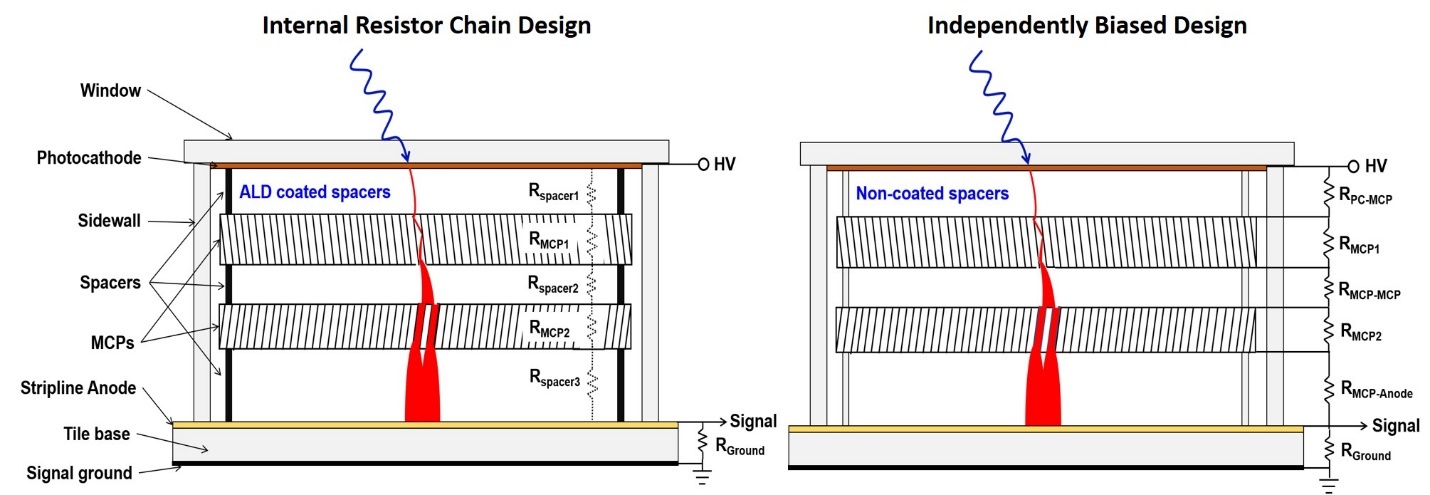
The internal resistor chain MCP-PMT design is adapted from the original LAPPDTM design [17]. The left panel of Figure 1 shows a schematic of the internal resistor chain MCP-PMT design. The sealed vacuum package consists of a photocathode, two MCPs, three grid spacers and a stripline anode. An air-sensitive alkali antimonide photocathode is deposited on the inside surface of the top glass window, and the electronic connection is provided by a pre-coated nichrome layer at the edges of the top window to apply high voltage. Two MCPs with pores of 8∘ bias angles are placed in chevron geometry to prevent drift of positive ions to the photocathode and to ensure a well-defined first strike of the incoming photoelectrons. The MCPs used here are sliced from the same ALD coated 20 20 cm2 MCPs used for LAPPDTM production, featuring a pore size of 20 m, a length to diameter (L:d) ratio of 60:1 and an open to full area ratio of 65%. Glass spacers are used between the photocathode and the top MCP, between the MCPs, and between the bottom MCP and the anode to separate individual components and support the stack configuration. The stripline anode is made through silk-screening of silver strips onto the glass tile base, and each stripline is grounded through a resistor. It is important to note that the MCPs and glass spacers are all coated with resistive materials via the ALD method, making the whole detector stack an internal resistor chain, as indicated by the dashed line circuit in Figure 1. When a single high voltage (HV) is applied to the photocathode, the applied HV is distributed between the internal components, controlled by the resistances of the ALD coated MCPs and glass spacers. Signals generated by incident photons are picked up from the stripline anodes and routed to an oscilloscope or an electronic waveform digitizer.
The internal resistor chain design only requires one HV connection from the outside to the inside of the vacuum as provided by the pre-coated nichrome mask on the top window. This simple design offers the advantage of ease of implementation and potentially low production cost. However, processing and testing of the fabricated MCP-PMTs reveal several drawbacks: (a) the HV distribution relies on the resistance ratios between the spacers and MCPs, where it is challenging to identify precisely matched resistances for the MCPs and spacers; (b) the fabrication of MCP-PMT requires thorough baking and scrubbing of the MCPs under vacuum for outgassing, while it has been shown that the resistances of ALD coated MCPs and spacers are reduced unevenly during this process, possibly resulting in mismatched resistances of MCPs and spacers; (c) once the detector is sealed, there is no way to individually optimize the MCP’s performance as the bias voltage on each MCP cannot be adjusted individually; (d) the absolute quantum efficiency (QE) of the photocathode cannot be measured using the traditional method as the photocurrent (nA level) generated from incident photons is dwarfed by the continuous bias current (A level) of the resistor chain.
2.2 Independently biased MCP-PMT design
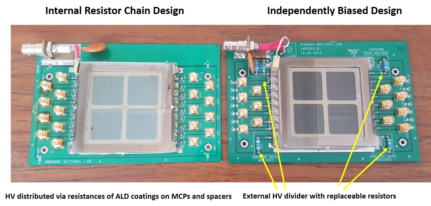
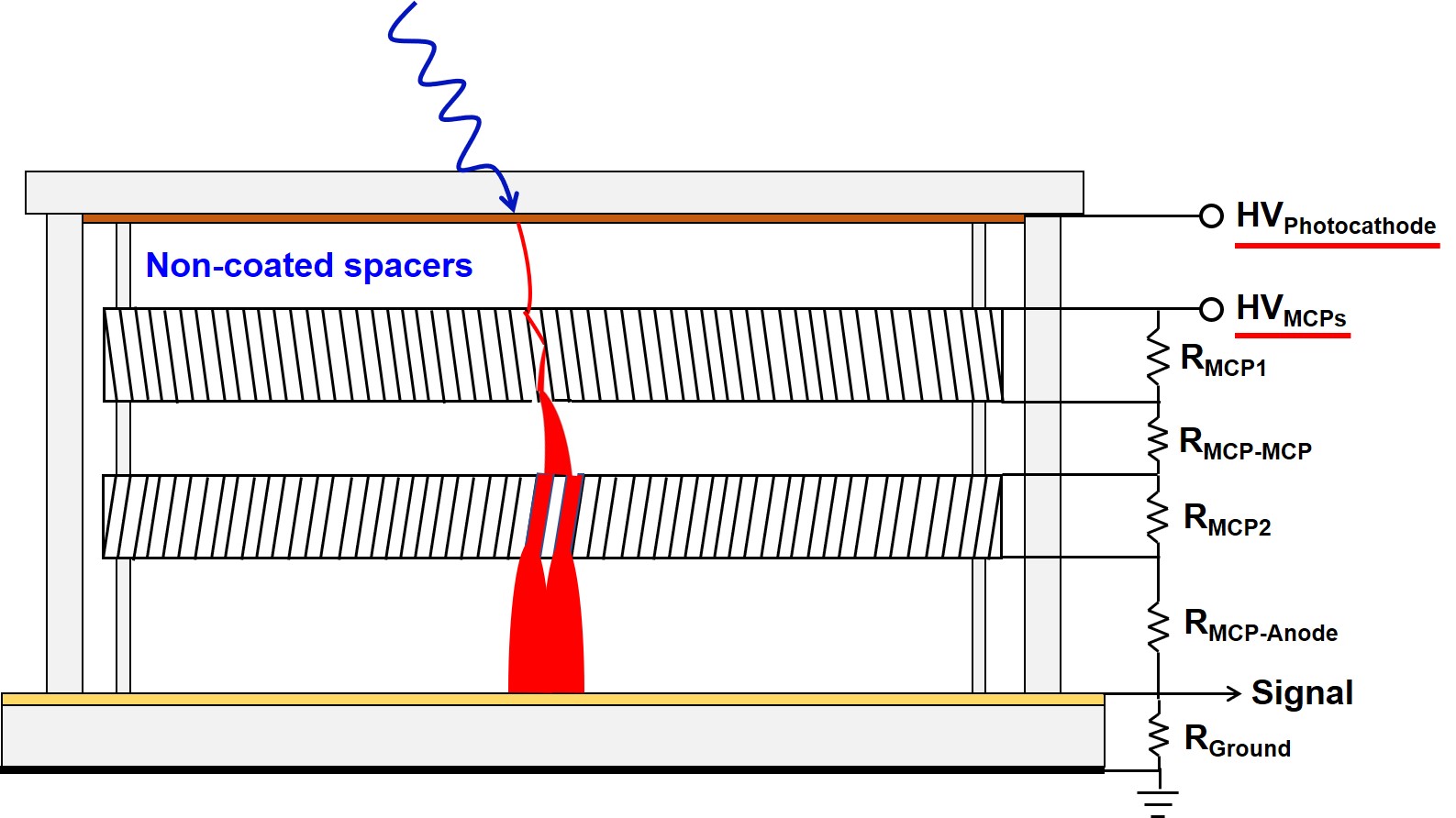
The independently biased MCP-PMT design (IBD) offers the option to optimize the performance of each MCP individually. A schematic of the new IBD configuration is shown in the right panel of Figure 1. The major differences compared to the previously described internal resistor design include: (1) the spacers are bare glass grids with no ALD coating on the surface, so the spacers can be treated as insulators; (2) ultra-thin stainless steel shims with the same pattern as grid spacers are attached between the spacers and the MCP surfaces to provide HV connections; (3) finger tabs are implemented on each shim, leading to the nearest silkscreen printed silver strip contact at one corner, which in turn provides the HV connection to the outside. Four shims are inserted between the upper and lower surfaces of the two MCPs. The new IBD design is based on a minimal modification of the internal resistor chain design, using shims and corner strip lines for the HV connection, while no pins are required to provide high voltage on the MCPs and in the gaps. Figure 2 shows a photograph of a sealed MCP-PMT based on the independently biased design (right). Simple readout circuit boards were designed and fabricated to hold the MCP-PMTs. An external resistor chain HV divider is integrated into the readout board of the independently biased MCP-PMT design so that only one HV source is necessary. The bias voltage of individual MCPs can be independently adjusted by altering the values of the corresponding resistors.
3 Magnetic field tolerance test facility
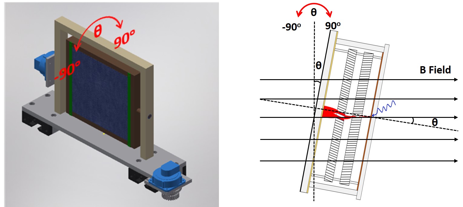
Argonne National Laboratory acquired a decommissioned superconducting magnet from a magnetic resonance imaging (MRI) scanner. The primary goal of this magnet is to perform the precise calibration of the various magnetic probes for the g-2 muon experiment [18]. The MRI magnet provides a large bore with a diameter of 68 cm and a very homogeneous field (7 ppb/cm), with a tunable magnetic field strength of up to 4 Tesla. We assembled a characterization system compatible with the solenoid magnet to test the performance of the 66 cm2 MCP-PMTs in strong magnetic fields of this magnet. A non-magnetic, light-tight dark box was built to contain the MCP-PMTs during their tests. The dark box was held on a platform with the detector surface normal to the direction of the magnetic field. The position of the dark box was adjusted so that the center of the MCP photodetector was aligned with the center of the solenoid magnet. A rotation mechanism was integrated into the system, able to rotate the MCP-PMTs by an angle (-90 90∘), as illustrated in Figure 3.
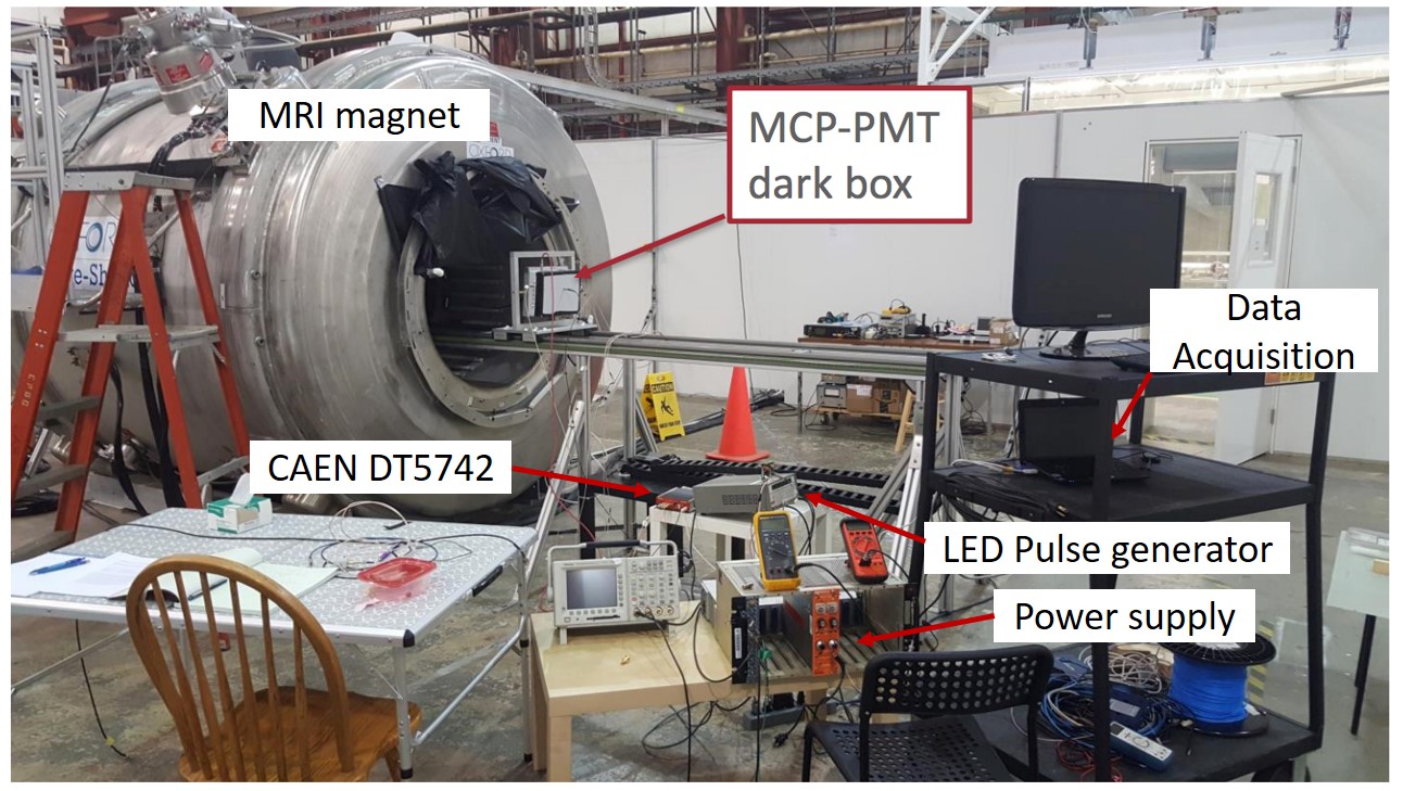
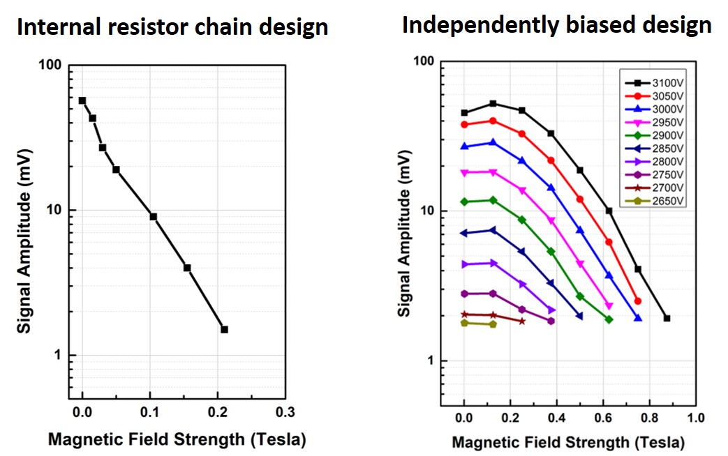
Figure 4 shows a picture of the entire magnetic field tolerance testing system. A 405 nm light-emitting diode (LED) driven by a pulse generator provided the light source. The light was guided into the dark box via an optical fiber. High voltage was applied to the MCP-PMTs from a power supply with continuous voltage control. Signals collected at the striplines were read out through a DT5742 desktop digitizer [19] with a sampling rate of 5 GS/s, as produced by CAEN (Costruzioni Apparecchiature Elettroniche Nucleari S.p.A.). The digitizer is based on a switched capacitor array of DRS4 (Domino Ring Sampler) chips [20] and features 16 analog input channels, and one additional analog input for a fast trigger.
A similar MRI magnet with tunable magnetic field up to 3 Tesla and a similar platform but without the rotation mechanism were available for MCP-PMT testing at the University of Virginia. The following measurements of the MCP-PMT based on the internal resistor chain design were performed at University of Virginia, while measurements of the MCP-PMT based on the independently biased design were performed at Argonne.
4 Results and discussion
The operational principle of MCP-PMTs relies on the electron multiplication process where the MCP pore walls are bombarded with secondary electrons. Each pore of the MCP has an internal diameter of 20 m with the inner wall processed with resistive and secondary emissive coating layers, which act as an independent electron multiplier. When the MCP-PMT is operated in a magnetic field, the trajectories of electrons during the electron multiplication process are affected by the Lorentz force due to the presence of both electric and magnetic fields. We studied the MCP-PMT performance as a function of magnetic field strength, rotation angle, and photocathode to MCP electric field strength.
4.1 Dependence on the magnetic field strength
The performance of MCP-PMTs based on the above two designs was tested in the magnetic field at a zero rotation angle , i.e., where the direction of the magnetic field is normal to the surface of the MCP photodetector. A 405 nm pulsed LED with a fixed light intensity corresponding to 10 photoelectrons was used as light source. The signal amplitude versus magnetic field strength is shown in Fig. 5.
The MCP-PMT based on the internal resistor chain design shows a poor magnetic field tolerance, the signal amplitude drops by a factor of 6 when the magnetic field increases from 0 to 0.1 Tesla, and another factor of 6 when the field increases to 0.2 Tesla. This rapid decrease is mainly due to the resistances of the MCPs and spacers having been significantly changed during the baking and scrubbing process, resulting in a bias voltage mismatch of the two MCPs. These results indicate that the MCP-PMT based on the resistor chain design is not suitable for applications in magnetic fields over 0.1 T.
On the other hand, the MCP-PMT based on the independently biased design shows a significantly improved tolerance to magnetic fields. The performance was measured at various magnetic field strengths and applying various bias high voltages. At a fixed magnetic field strength, the signal amplitude increases with increasing bias high voltage. This behavior confirms our previous measurements of MCP-PMTs in a negligible magnetic field [21]. At a fixed bias voltage of 3100 V, the signal amplitude of the MCP-PMT increases slightly as the magnetic field strength increases to 0.2 T, and then is seen to decrease as the magnetic field strength continues to increase, and eventually is reduced below 5 mV at a magnetic field strength of 0.7 T. With lower bias voltages, the signal amplitudes are seen to be reduced already at lower field strength. As these results show, the decrease in signal strength can to some extend be compensated by increased bias voltages.
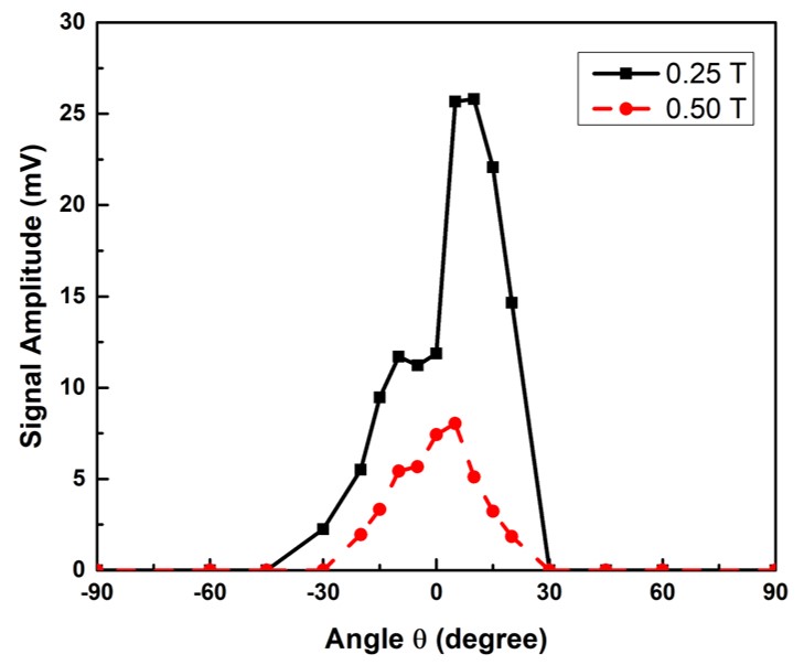
4.2 Dependence on the tilt angle
The signal strength as function of tilt angle between the normal to the MCP-PMT window and the direction of the magnetic field, as shown in Figure 3, was investigated using the MCP-PMT based on the independently biased design. We applied a fixed high voltage of 3000 V and rotated the tilt angles from -90∘ to 90∘. Figure 6 shows the signal amplitude as a function of the tilt angle for two magnetic field strengths of 0.25 and 0.5 Tesla, respectively. The signal amplitude shows a strong angle dependence with vanishing signals outside the range of -3030∘ and two maxima at 8∘. The latter are related to the 8∘ bias angle of the MCP pores and their chevron configuration. When the direction of one MCP pore is aligned with the direction of the magnetic field, the MCP-PMT shows an enhanced magnetic field tolerance. The signal maximum at +(-)8∘ corresponds to the position where the direction of the pores of the top (bottom) MCP is aligned with the direction of the magnetic field.
4.3 Dependence on the gap high voltage
The MCP-PMTsignal amplitude as a function of applied HV to the gap between the photocathode and the top MCP was studied at different magnetic field strengths. Figure 7 shows the circuit diagram which allowed to vary the applied gap voltage. While the HVMCPs was kept at a fixed value, the HVPhotocathode was varied to adjust the gap voltage.
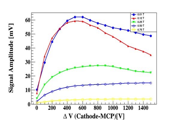
Figure 8 shows the signal amplitude versus gap voltage for a selection of magnetic field strengths. With low magnetic fields, the signal amplitude increases as the gap voltage increases and reaches a maximum at a gap voltage of 500 V. Further increasing the gap voltage beyond 500 V results in a decreasing signal amplitude. This effect is related to the energy of the primary electrons, as studied previously [22]. As these studies showed, the yield of secondary emissions of ALD coated materials is highest when the primary electron energy is around 300 – 500 eV, corresponding to a gap HV at 500 V. With higher primary electron energies, the electrons penetrate deeper into the coating, thus again reducing the yield of secondary emission electrons. At high magnetic fields, the magnetic field strength becomes the main parameter affecting the secondary emission process. The secondary yield is not seen to decrease anymore with primary electron energy over 500 eV, resulting in a continuously increasing signal amplitude with increasing gap voltages.
5 Conclusions
Two 66 cm2 MCP-PMTs based on the internal resistor chain design and the independently biased design were fabricated at Argonne National Laboratory and characterized in magnetic fields. The behavior of the MCP-PMT signal amplitude was investigated as a function of the magnetic field strength, the distribution of bias voltage, the tilt angle, and the gap voltage. It was found that the MCP-PMT based on the internal resistor chain design shows a magnetic field tolerance only up to 0.1 T. With the independently biased voltage design, the magnetic field tolerance of the MCP-PMT is significantly improved, up to 0.7 T. These findings indicate the importance of ensuring that both MCPs are operated at their optimal bias voltages when operated in high magnetic fields. As the magnetic field strength increases, the signal amplitude of the MCP-PMT decreases while being operated at a constant bias voltage. However, the reduction of signal amplitude can be compensated by increasing the operation voltage, extending the range of operability in high magnetic fields. Due to the original MCP bias angle of 8∘ and the chevron configuration, the pores of both MCPs can not be aligned simultaneously with the direction of the magnetic field. The MCP-PMT shows higher signal amplitudes when either MCP pores is aligned with the direction of the magnetic field, where the direction of the top MCP pores exhibits a stronger impact on the signal amplitude. Increasing the bias voltage applied on the gap between the photocathode and the top MCP results in a maximum signal amplitude with gap voltage around 500 V at low magnetic fields, while a continuously increasing signal amplitude is observed at high magnetic fields.
6 Acknowledgments
The authors thank Frank Skrzecz (Engineer at ANL) for his mechanical engineering support; Joe Gregar (Scientific Glass Blower at ANL) for his talented work on glass parts; Mark Williams and Wilson Miller (Professors at University of Virginia) for their arrangement of the University of Virginia MRI magnet usage; Peter Winter (Physicist at ANL) for his arrangement of the Argonne 4-Tesla magnetic facility usage; and many people from the LAPPD collaboration for their advice and assistance. This material is based upon work supported by the U.S. Department of Energy, Office of Science, Office of High Energy Physics, Office of Nuclear Physics, under contract number DE-AC02-06CH11357. Work at Thomas Jefferson National Accelerator Facility was supported by the U. S. Department of Energy, Office of Science under contract No. DE-AC05-06OR23177. Work at Brookhaven National Laboratory was supported by the U. S. Department of Energy, Office of Science under contract No. DE-SC0012704. This work was also partially supported by the EIC R&D funding from the Office of Nuclear Physics and Office of Science of the U.S. Department of Energy.
References
- [1] A. Accardi, et al., Electron ion collider: The next QCD frontier, Eur. Phys. J. A 52 (2016) 268.
- [2] A. Aprahamian, et al., Reaching for the horizon: The 2015 long range plan for nuclear science (2015).
- [3] A. Kiselev, BeAST Detector (Brookhaven eA Solenoidal Tracker), presentation on Electron Ion Collider User Group Meeting, Berkeley, CA (2016).
- [4] PHENIX Collaboration, Concept for an Electron Ion Collider (EIC) detector built around the BaBar solenoid, arXiv:1402.1209.
- [5] G. Wei, et al., Integration of the full-acceptance detector into the JLEIC, Proceedings of IPAC2017, THPAB084, Copenhagen, Denmark (2017).
- [6] J. Repond, TOPSiDE – Concept of an EIC Detector, Workshop on Streaming Readout, Boston, MA (2018).
- [7] J. L. Wiza, Microchannel plate detectors, Nucl. Instr. and Meth. A 162 (1979) 587.
- [8] B. Adams, et al., A brief technical history of the Large-Area Picosecond Photodetector (LAPPD) Collaboration, (2016) arXiv:1603.01843.
- [9] M. Minot, et al., Pilot production & commercialization of LAPPD, Nucl. Instr. and Meth. A 787 (2015) 78.
- [10] A. U. Mane, et al., An atomic layer deposition method to fabricate economical and robust large area microchannel plates for photodetectors, Physics Procedia, 37 (2012) 722.
- [11] M. Popecki et al., Microchannel plate fabrication using glass capillary arrays with atomic layer deposition films for resistance and gain, J. Geophys. Res. Space Phys., 121 (2016) 7449.
- [12] A. O’Mahony et al., Atomic layer deposition of alternative glass microchannel plates, J. Vac. Sci. Tech., 34 (2016) 01A128.
- [13] T. M. Conneely, J. S. Milnes, and J. Howorth, Extended lifetime MCP-PMTs: Characterisation and lifetime measurements of ALD coated microchannel plates, in a sealed photomultiplier tube, Nucl. Instr. and Meth. A 732 (2013) 388.
- [14] O. H. W. Siegmund, et al., Performance characteristics of atomic layer functionalized microchannel plates, Proc. SPIE 8859, (2013) 88590Y.
- [15] J. Xie, et al., Development of a small form-factor 6 x 6 cm2 picosecond photodetector as a path towards the commercialization of large area devices, Proceeding of The Technology and Instrumentation in Particle Physics 2014, PoS (2014).
- [16] Incom, Inc.: http://www.incomusa.com/
- [17] B. Adams, et al., Measurements of the gain, time resolution, and spatial resolution of a large 20 x 20 cm2 MCP-based picosecond photo-detector, Nucl. Instr. and Meth. A 732 (2013) 392.
- [18] 4 Tesla Magnet Facility: https://www.anl.gov/hep/group/4-tesla-magnet-facility
- [19] DT5742 desktop digitizer: http://www.caen.it
- [20] DRS chip developed at Paul Scherrer Institute, Switzerland: https://www.psi.ch/drs
- [21] J. Wang et al., Development and testing of cost-effective, 6 x 6 cm2 MCP-based photodetectors for fast timing applications, Nucl. Instr. and Meth. A 804 (2015) 84.
- [22] S. Jokela et al., Secondary electron yield of emissive materials for large-area micro-channel plate detectors: surface composition and film thickness dependencies, Physics Procedia 37 (2012) 740.