Exchange interaction of magnetic impurities in biased bilayer phosphorene nanoribbon
Abstract
We study Ruderman-Kittel-Kasuya-Yosida (RKKY) interaction, in zigzag bilayer phosphorene nanoribbons (ZBLPNRs) under a perpendicular electric field. We evaluate the spatial and electric field dependency of static spin susceptibility in real space in various configurations of magnetic impurities at zero temperature. The electronic properties of ZBLPNR in the presence of a gate voltage is also obtained. In comparison to the other two-dimensional (2D) materials such as graphene, silicene and etc, ZBLPNR has two nearly degenerated quasiflat edge modes at the Fermi level, isolated from the bulk states. The band gap modulation of ZBLPNRs by the ribbon width and perpendicular electric field is investigated. Due to the existence of these quasiflat bands at the Fermi level, in the absence of the electric field, a sharp peak in the RKKY interaction is seen. As shown, the signatures of these unique quasiflat edge modes in ZBLPNRs could be explored by using the RKKY interaction. In the presence of a large bias potential a beating pattern of the RKKY oscillations occurs for when two magnetic impurities located inside the ZBLPNR. The electrically tunable RKKY interaction of ZBLPNRs is expected to have important consequences on the spintronic application of biased ZBLPNR.
I Introduction
Black phosphorus (BP) monolayer, called phosphorene, has emerged as a promising material in the field of optoelectronics and magnetoelectronics of 2D systems Li14 ; Liu14 ; andre ; Xia14 ; Moslem-bp ; Carvalho16 ; Batmunkh . Phosphorene has a puckered honeycomb structure due to the hybridization Liu15 ; Das14 ; Kamalakar15 ; Lu14 ; Fei14 ; Wang1 ; Moslem-bp . Its conventional unit cell, consists of atoms with the lattice constants Å and Å in (zigzag) and (armchair) directions, respectively. Structural anisotropy of phosphorene makes its thermal, electrical and optical properties zare-bp ; Liu14 ; Fei14 ; Tran14 , a high degree of anisotropy. Charge carriers in phosphorene exhibit exceptionally high carrier mobilities at room temperature cm2 V-1 s-1 Li14 ; Liu14 which exhibits a strongly anisotropic behavior in the phosphorene-based field effect transistor with a high on/off ratio, Liu14 . Moreover, by changing the number of layers and applying strain and external field, the direct bandgap of BP multilayer systems can be varied, spanning the losing gap between graphene and other 2D materials Liu14 ; Du10 ; Tran14 ; cakir14 ; Liang14 ; Rodin14 . As the layer number strongly affects the physical properties of 2D black phosphorus multilayers, it is of both fundamental and practical interest to study the effect of the interlayer coupling on these physical properties. In this regard, bilayer phosphorene (BLP) is an appropriate candidate that can provide basic information on this coupling effect.
In the last decade, dilute semiconductors have emerged as a research hotspot due to their unique and new functionalities. In this regard, utilizing phosphorene may be lead to next generation of spintronic devices based on the spin degrees of freedom fabian ; Babar .
Nonmagnetic nature of the pristine semiconductor phosphorene limits its applications in the field of magnetoelectronics and spintronics. Phosphorene can be magnetized in several ways such as doping with non-magnetic adatoms Zheng15 ; Yang16 ; khan15 , edge cutting Zhu14 ; Du15 ; Farooq15 ; Farooq16 ; Xu16 , and inserting atomic defects and vacancies on phosphoreneSrivastava15 ; Suvansinpan16 ; Babar . Phosphorene nanoribbons with bare zigzag edges are antiferromagnetic semiconductors Du15 . This magnetization also opens a significant direct band gap (about 0.7 eV), which transforms the metallic PNRs into semiconductors ones.
Most effective approach to induce magnetization with large Curie temperature is the adsorption or substitutional doping of transition-metal atoms on phosphorene Zhai17 ; Khan16 ; Kulish ; Seixas15 ; Sui15 . As the transition-metal atoms interact much stronger with phosphorene, compared to the other two dimensional materials such as graphene, it becomes more probable to turn the pristine phosphorene into a ferromagnetic or antiferromagnetic material Kulish . Strength of these created magnetic moments depends on the metal species and the result can be tuned by the applied strain Hu15 ; Sui15 ; Seixas15 ; Yu16 ; Cai17 .
Ruderman-Kittel-Kasuya-Yosida (RKKY) exchange interaction Ruderman ; Kasuya ; Yosida , a fundamental interaction for spintronic applications, is mediated by a background of conduction electrons of the host material. It is the most important mechanism of the coupling between magnetic impurity dopants in metals and semiconductors. As an applied point of view, this interaction can lead a magnetically doped system to interesting phases such as ferromagnetic Vozmediano ; Brey ; Priour ; Matsukura ; Ko ; Ohno-science , antiferromagnetic Minamitani ; Loss15 , spiral moslem-si ; Mahroo-RKKY and spin-glass pesin ; Eggenkamp ; Liu87 . Besides the practical importance of the RKKY interaction in the possible magnetic phases of semiconductor, it can provide information about the intrinsic properties of the material since this coupling is proportional to the spin susceptibility of the host system. While this interaction falls off by , where is the dimension of the system fariborz-blg ; fariborz-mos2 , it oscillates with the Fermi wavevector originates from the Friedel oscillations. In systems with multiband structure fariborz-mos2 or with spin polarization fariborz-sp , these oscillations become more complicated than a monotonic oscillation with behavior, where is the wave vector of the electrons (holes) at the Fermi level and is the distance of two magnetic impurities. Moreover, it has been shown that the magnitude of the RKKY interaction can be severely affected by the density of states (DOS) at the Fermi energy fariborz-blg ; Mahroo-RKKY . In addition, it can be sensitive to the direction of the distance vector between impurities in materials such as graphene sherafati-g ; fariborz-blg owing to the bipartite nature of the honeycomb sublattice. In materials with Rashba spin-orbit coupling, the spin response of the system to the magnetic impurity depends on the direction of the magnetic moment Mahroo-single and as the result the RKKY interaction becomes anisotropic Mahroo-RKKY .
RKKY interactions in nanoribbon of two dimensional lattices has attracted strong attention in condensed matter physics moslem-si ; Klinovaja13 ; Moslem18 ; Duan17 . Recently, in a detailed study it has shown that the topological phase transition in the zigzag silicene nanoribbon can be probed by using the RKKY interaction moslem-si . In another work, it has concluded that the RKKY interaction in the bulk phosphorene monolayer is highly anisotropic and the magnetic ground-state of two magnetic adatoms can be tuned by changing the spatial configuration of impurities as well as the chemical potential varying Moslem18 . Duan et.al also study the effect of strain on the magnetic impurity interactions in phosphorene Duan17 . Very recently, the effect of tensile strain on the RKKY interaction in the biased monolayer phosphorene nanoribbon is studied, numerically Moldovan . They showed how one could isolate the edge state from that of the bulk contribution using the RKKY interaction, by tuning the external gate potential. In this paper, we present the Green’s function technique for derivation of RKKY interaction in a biased bilayer phosphorene nanoribbon. Also, we show that by changing the perpendicular electric field due to the band structure changing one can drastically change the interaction between impurities, which can be a great way to control magnetic properties by electric field.
This paper is organized as follows. In Sec. II, we introduce a tight-binding model Hamiltonian for biased bilayer phosphorene and then calculate the band spectrum of ZBLPNR under the vertical electric field. Here we introduce the theoretical framework which will be used in calculating the RKKY interaction from the real space Green’s function. In Sec. III, we discuss our numerical results for the proposed magnetic doped ZBLPNR in the presence of a perpendicular electric field. Finally, our conclusions are summarized in Sec. IV.
II Theory and model
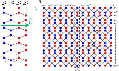
As the Bernal stacking configuration of two phosphorene layers, coupled via the van der Waals interaction, is energetically most stable form of the bilayer phosphorene Peeters15 ; Jhun17 , we consider an AB stacked ZBLPNR as shown in Fig. 1. In the presence of an uniform perpendicular electric field, low-energy carriers in BLP are described by the following tight-binding(TB) Hamiltonian Moldovan ; Rudenko2016 ; Dolui16 :
| (1) |
where the summation runs over all lattice sites of the system. () is the creation (annihilation) operator of an electron at site (), is the on-site energy at site and () is the intralayer (interlayer) hopping energy between sites and . The relevant hopping parameters considered by Li et.al Moldovan , are two in-plane hopping terms () and a interlayer term. In the presence of a perpendicular electric field, the four atomic sublayers in BLP will earn different on-site electrostatic potentials in the form of , , , and , where is the electrostatic potential energy difference between the top and bottom phosphorene layers, with the elementary charge, the electric field strength, the interlayer separation, and is a linear scaling factor that accounts for the sublayer dependence of the on-site electrostatic potential Yuan16 .
The geometry of a ZBLPNR with zigzag edges is illustrated in Fig.1. Its conventional unit cell, consists of atoms with the lattice constants and in (zigzag) and (armchair) directions, respectively exactly equal to the monolayer phosphorene lattice constants. Here, the unit cell used in the tight-binding calculations of the ZBLPNR (dashed rectangle), containing atoms, is also indicated. The respective unit cell width is . For simplicity, as shown in this figure each atom labeled with a set , which represent the and coordinates of the lattice points. In our analysis, we consider the two magnetic impurities located at and sites of the nanoribbon (following the notations of Fig.1). In this ribbon geometry, it is easy to find the energy dispersion with the periodic boundary condition along the ribbon’s zigzag edge in the direction. Owing to the translational invariant along the ribbon edges , the momentum in the direction is a good quantum number. To study the band structure properties provided by our tight-binding model, we find its space forms as . Applying Bloch’s theorem, performing the Fourier transformation along the direction, the Hamiltonian in space can be written as
| (2) |
in which is the lattice constant along the zigzag direction. Moreover, and describe coupling matrix within the principal unit cells (intralayer), with odd and even indices , respectively and denotes the effective coupling between two adjacent unit cells (interlayer), based on the tight-binding model given by Eq. (1).
The energy dispersion and the wavefunctions can also be obtained by diagonalizing the Hamiltonian for the nearest-neighbor tight-binding model. In order to calculate the site-resolved local density of states (LDOS) for the ribbon as , for -th site. In order to do so, corresponding wave function for a given energy and wave vector might be first obtained.
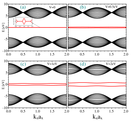
The calculated band structures of ZPNRs are shown in Figs.2. In similarity with ZPNR, ZBLPNRs have two nearly degenerated quasiflat edge modes at the Fermi level Ajanta16 ; Ezawa14 ; Taghizadeh15 ; Ma16 ; Ostahie16 that are entirely detached from the bulk band. By applying the electric field the band degeneracy breaks. The properties of edge states in ZBLPNRs are essentially different from the other 2D zigzag nanoribbons. In comparison with ZBLPNR and ZPNR, in 2D Dirac materials such as graphene and silicene, the edge modes merge into the bulk band at the two Dirac points. Degeneracy of these two quasi flat bands is broken by applying a perpendicular electric field. As recently addressed by Ezawa Ezawa14 , the origin of this decoupled matter of the flat edge modes is the presence of two out-of plane zigzag chains, coupled by a relatively strong hopping parameter.
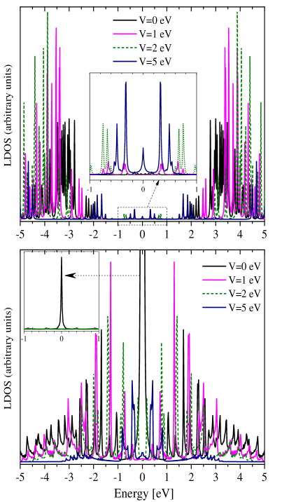
Figure 3 displays the LDOS of phosphorus atoms in either sublattice at the edge or in the bulk. The top panel presents the LDOS of the bulk configuration at the site , and the bottom one presents the edge configuration at the site . Similar to the ZPNR Firoz18 , when the applied gate voltage is zero the LDOS shows a sharp peak around the zero energy corresponding to edge states, in comparison to the bulk.
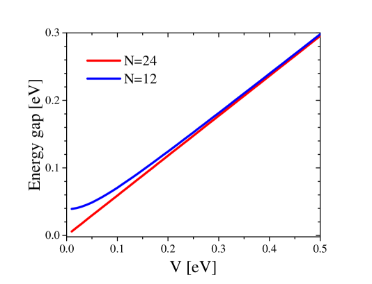
Moreover, figure 4 shows the energy gap of the ZBLPNR as a function of the applied electric field. As previously obtained, the energy gap increases linearly as the applied electric field is increased Yang16 . The zero biased gap decreases with increasing ribbon width and tends to zero in the limit of very large . The carrier-mediated exchange coupling between the spin of itinerant electrons and two magnetic impurities with magnetic moments and , located respectively at and , is given by
| (3) |
where are the conduction electron spin densities at positions and and is the coupling between the impurity spins and the itinerant carriers.
In the linear response regime, the interaction energy between the two localized magnetic moments may be written as a Heisenberg form Ruderman ; Kasuya ; Yosida ; Imamura
| (4) |
The RKKY interaction is explained using the susceptibility, the response of the charge density to a perturbing potential ,
| (5) |
where is the charge susceptibility for a crystal, is a spin-independent perturbing potential and is the induced charge density.
The static spin susceptibility can be written in terms of the integral over the unperturbed Green’s function
| (6) |
where is the Fermi energy. The expression for the susceptibility may be obtained by using the spectral representation of the Green’s function
| (7) |
where is the sublattice component of the unperturbed eigenfunction with the corresponding energy . For a crystalline structure, denotes the band index and spin. In other words, it just denotes a complete set of quantum states. Substituting Eq. (7) into Eq. (6), we get the result
| (8) |
After exchanging the dummy variables and , the imaginary part of the product of the four wave functions appearing in the equation above is odd, while its real part is even, and at the same time, both the imaginary and the real parts of the product of the energy-space Green’s function are even. By applying this property the second expression becomes zero. Finally, the reads as
| (9) |
in which
| (10) |
To prove the above equality we use the relationship . The integration over energy can be carried out next, leading to our desired result
| (11) | |||||
where, , is the Fermi function. This is a well-known formula in the linear response theory that is the main equation in this work. It is worth mentioning that under the interchange of , and , the summand in Eq. (11) converts to its complex conjugate, so that only the real part survives.
III numerical results
In this section, we present our main results for the RKKY exchange coupling in the zigzag bilayer phosphorene nanoribbons presence of perpendicular electric field. In order to do so, we evaluate static spin susceptibility Eq. (11), in real space in various configurations of magnetic impurities at various bias voltages.
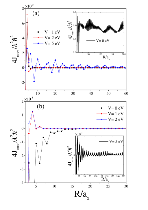
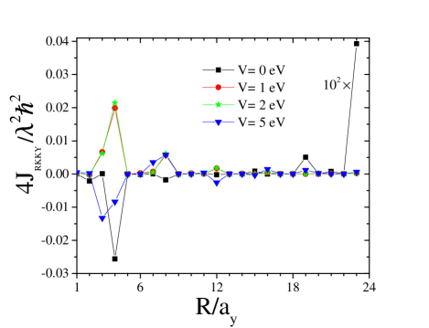
Figure 5 shows the spatial behavior of the RKKY interaction for two impurities, (a) both sitting on the same edge along the line (b) both located inside the zigzag nanoribbon (away from the edges) along the line for different bias voltages for a ZBLPNR with . As indicated, in the case of both impurities located at an edge, in the moderate fields, the RKKY interaction displays an oscillatory behavior in and decays fast with a short-ranged behavior. More interestingly, by applying the electric field the RKKY interaction strength dramatically quenched (in the zero field regime (), the RKKY interaction is about five orders of magnitude greater). The reason for that is related to the existence of nearly-zero-energy states at the edge of the ZBLPNR. In the high field regime (), the RKKY interaction shows a long-range oscillatory behavior in , because the Fermi energy crosses the bulk bands. Similar to the ZPNR Firoz18 , the RKKY coupling attains its maximum strength when the applied gate voltage is zero. The contribution of the bulk states are nearly zero as the impurities are located at the edge of the ZBLPNR.
Otherwise, when both the impurities are sited in the interior region of the ZBLPNR, no difference in the order of magnitude appears for different bias voltages (see figure 5(b)). In similarly with the edge configuration of the impurities (both located on the same edge), RKKY shows a few oscillations in , then it decays fast with a short-ranged behavior. More interestingly, in the presence of a large bias potential (), a beating pattern of oscillations of the RKKY interaction occurs for when two magnetic impurities located inside the ZBLPNR. The beating feature originated from the crossing the Fermi energy and the bulk bands for the bulk impurities (both moments located inside the ZBLPNR).
Figure 6 shows the spatial behavior of the RKKY interaction for when the first impurity is fixed at the edge at sublattice and the second one is moved along the line with coordinates , where . As in the absence of the applied bias, () the exchange coupling is approximately two orders of magnitude greater than the case with potential (), for the better clarity we multiply the values related to the zero bias by . In the case of zero bias, for both impurities located at an armchair chain (both located in the same ZBLPNR unit cell), the largest coupling appear when both moments is located at two counterpart edge sublattices.
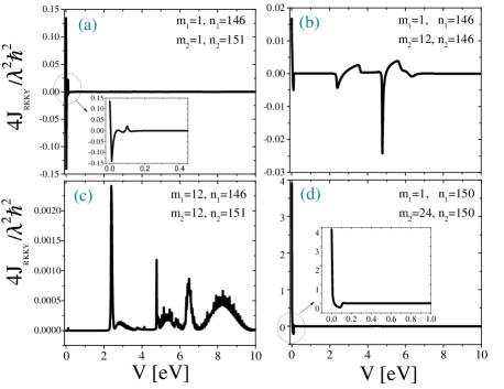
Figures 7(a-d) show the numerical results for the RKKY coupling as a function of bias voltage for different configurations of magnetic impurities. (a) when two impurities are fixed at the same zigzag edge at and lattice points. Turning on the electric field, a sudden fall off in the RKKY interaction strength occurs, because the zero-energy state at the edge of the ZBLPNR is suddenly dropped. This behavior is also seen for when both moments are located at two counterpart edge sublattices (figure 7(d)) because by turning on the electric field, the edge modes in ZBLPNR become fully separated from the bulk. This unique nature of the edge states in ZBLPNR allows us to probe them separately from the bulk. Numerical results for when the first impurity is fixed at the zigzag edge at and the second one located inside the ZBLPNR at lattice point, is shown in figure 7(b). Figure 7(c) shows the RKKY coupling for two impurities fixed inside the ZBLPNR at and lattice points.
IV summary
.
We study Ruderman-Kittel-Kasuya-Yosida interaction, in zigzag bilayer phosphorene nanoribbons (ZBLPNRs) under a perpendicular electric field. For this, we evaluate the spatial and electric field dependency of static spin susceptibility in real space in various configurations of magnetic impurities at zero temperature. We evaluate this interaction from the Green’s function approach based on the tight-binding model Hamiltonian. The electrically tunable RKKY interaction of ZBPNRs is expected to have important consequences on the spintronic application of biased ZBLPNRs. The electronic property of ZBLPNR in the presence of gate voltage is also obtained. In comparison to the other 2D materials such as graphene, silicene and etc, ZBLPNRs have two nearly degenerated quasiflat edge modes at the Fermi level in a ZBLPNR, isolated from the bulk states. A gap occurs by applying a perpendicular electric field. As shown, the signatures of these unique quasiflat edge modes in ZBLPNRs could be explored by using the RKKY interaction. Due to the existence of the quasiflat bands at the Fermi level, in the absence of the electric field, a sharp peak in the RKKY interaction is seen. By varying the width of the phosphorene ribbons, we find that the size effect is crucial for determining the relative importance of the edge state.Moreover, figure 4 shows the energy gap of the ZBLPNR as a function of the applied electric field. As previously obtained, the energy gap increases linearly as the applied electric field is increased Yang16 . The zero bias gap decreases with increasing ribbon width and tends to zero in the limit of very large . In the presence of a large bias potential a beating pattern of oscillations of the RKKY interaction occurs for when two magnetic impurities located inside the ZBLPNR.
ACKNOWLEDGMENT
This work is partially supported by Iran Science Elites Federation.
References
References
- (1) L. Li, Y. Yu, G. J. Ye, Q. Ge, X. Ou, H. Wu, D. Feng, X. H. Chen and Y. Zhang, Nat. Nanotechnol. 9, 372 (2014).
- (2) H. Liu, A. T. Neal, Z. Zhu, Z. Luo, X. Xu, D. Tomanek, and P. D. Ye, ACS Nano 8, 4033 (2014).
- (3) A. Castellanos-Gomez, Nat. Photonics 10 202 (2016).
- (4) F. Xia, H. Wang, D. Xiao, M. Dubey, and A. Ramasubramaniam, ibid, 8, 899 (2014).
- (5) M. Zare, L. Majidi and R. Asgari, Phys. Rev. B 96, 115426 (2017).
- (6) X. Z. A. R. H. S. A. Carvalho, M. Wang and A. C. Neto, Nature Reviews Materials 1, 16061 (2016).
- (7) M. B.-E. M. Batmunkh and J. Shapter, Advanced Mate- rials 28, 8586 (2016).
- (8) H. Liu, Y. Du, Y. Deng, P. D. Ye, Chem. Soc. Rev. 44, 2732 (2015).
- (9) S. Das, M. Demarteau, A. Roelofs, ACS Nano 8, 11730 (2014).
- (10) M. V. Kamalakar, B. N. Madhushankar, A. Dankert, S. P. Dash, Small 11, 2209 (2015).
- (11) W. Lu, H. Nan, J. Hong, Y. Chen, C. Zhu, Z. Liang, X. Ma, Z. Ni, C. Jin, and Z. Zhang, Nano Res. 7, 853 (2014).
- (12) X. Wang, A. M. Jones, K. L. Seyler, V. Tran, Y. Jia, H. Zhao, H. Wang, L. Yang, X. Xu, and F. Xia, Nat. Nanotechnol. 10, 517 (2015).
- (13) R. Fei and L. Yang, Nano Lett. 14, 2884 (2014).
- (14) M. Zare, B. Z. Rameshti, F. G. Ghamsari, and R. Asgari, Phys. Rev. B 95 045422 (2017).
- (15) V. Tran, R. Soklaski, Y. Liang, and L. Yang, Phys. Rev. B 89, 235319 (2014).
- (16) Y. Du, C. Ouyang, S. Shi, and M. Lei, J. Appl. Phys. 107, 093718 (2010).
- (17) D. Çakir, H. Sahin, and F. M. Peeters, Phys. Rev. B 90, 205421 (2014).
- (18) L. Liang, J. Wang, W. Lin, B. G. Sumpter, V. Meunier, and M. Pan, Nano Lett. 14, 6400 6406 (2014).
- (19) A. S. Rodin, A. Carvalho, and A. H. Castro Neto, Phys. Rev. Lett. 112, 176801 (2014).
- (20) I. Zutić, J. Fabian, and S. Das Sarma, Rev. Mod. Phys. 76, 323 (2004).
- (21) R. Babar and M. Kabir, J. Phys. Chem. C 120, 27 (2016).
- (22) H. Zheng, J. Zhang, B. Yang, X. Du, and Y. Yan, Phys. Chem. Chem. Phys. 17, 16341 (2015).
- (23) L. Yang, W. Mi, and X. Wang, J. Alloys Compd. 662, 528 (2016).
- (24) I. Khan and J. Hong, New J. Phys. 17, 023056 (2015).
- (25) Z. Zhu, Ch. Li, W. Yu, D. Chang, Q. Sun, and Y. Jia, Appl. Phys. Lett. 105, 113105 (2014).
- (26) Y. Du, H. Liu, B. Xu, L. Sheng, J. Yin, C.-G. Duan, and X. Wan, Sci. Rep. 5, 8921 (2015).
- (27) M. U. Farooq, A. Hashmi, and J. Hong, ACS Appl. Mater. Interfaces 7, 14423 (2015).
- (28) M. U. Farooq, A. Hashmi, and J. Hong, Sci. Rep. 6, 26300 (2016).
- (29) G. Yang, S. Xu, W. Zhang, T. Ma, and C. Wu, Phys. Rev. B 94, 075106 (2016).
- (30) P. Srivastava, K. Hembram, H. Mizuseki, K. Lee, S. Han, and S. Kim, J. Phys. Chem. C 119, 6530 (2015).
- (31) N. Suvansinpan, F. Hussain, G. Zhang, C. Chiu, Y. Cai, and Y.-W. Zhang, Nanotechnology 27, 065708 (2016).
- (32) C. Zhai, X. Dai, W. Li, Y. Ma, T. Wang, and Y. Tang, Superlattices Microstruct. 49, 101 (2017).
- (33) I. Khan and J. Hong, Nanotechnology 27, 385701 (2016).
- (34) V. V. Kulish, O. I. M. andC. Persson, and P. Wu, Phys. Chem. Chem. Phys. 17, 9921000 (2014).
- (35) L. Seixas, A. Carvalho, and A. H. Castro Neto, Phys. Rev. B 91, 155138 (2015).
- (36) X. Sui, C. Si, B. Shao, X. Zou, J. Wu, B.-L. Gu, and W. Duan, J. Phys. Chem. C 119, 10059 (2015).
- (37) T. Hu and J. Hong, J. Phys. Chem. C 119, 8199 (2015).
- (38) W. Yu, Z. Zhu, C. Niu, C. Li, J. Cho, and Y. Jia, Nanoscale Res. Lett. 11, 77 (2016).
- (39) X. Cai, C. Niu, J. Wang, W. Yu, X. Ren, and Z. Zhu, Phys. Lett. A 381, 14 (2017).
- (40) M. A. Ruderman and C. Kittel, Phys. Rev. 96, 99 (1954).
- (41) T. Kasuya, Prog. Theor. Phys. 16, 45 (1956);
- (42) K. Yosida, Phys. Rev. 106, 893 (1957).
- (43) M. A. H. Vozmediano, M. P. Lopez-Sancho, T. Stauber, and F. Guinea, Phys. Rev. B 72, 155121 (2005).
- (44) L. Brey, H.A. Fertig, and S. Das Sarma, Phys. Rev. Lett. 99, 116802 (2007).
- (45) D. J. Priour, Jr., E. H. Hwang and S. Das Sarma, Phys. Rev. Lett. 92, 117201 (2004).
- (46) F. Matsukura, H. Ohno, A. Shen and Y. Sugawara, Phys. Rev. B 57, 2037(R) (1998).
- (47) K. T. Ko, Kyoo Kim, Sung Baek Kim, H. D. Kim, J. Y. Kim, B. I. Min, J. H. Park, F. H. Chang, H. J. Lin, A. Tanaka, and S. W. Cheong, Phys. Rev. Lett. 107, 247201 (2011)
- (48) H. Ohno, Science 281, 951 (1998).
- (49) E. Minamitani, W. A. Dino, H. Nakanishi, and H. Kasai, Phys. Rev. B 82, 153203 (2010).
- (50) C.-H. Hsu, P. Stano, J. Klinovaja, and D. Loss, Phys. Rev. B 92, 235435 (2015).
- (51) M. Zare, F. Parhizgar, and R. Asgari, Physical Review B 94, 045443 (2016).
- (52) M. Shiranzaei, H. Cheraghchi, and F. Parhizgar, Phys. Rev. B 96, 024413 (2017).
- (53) D. A. Abanin and D. A. Pesin, Phys. Rev. Lett. 106, 136802 (2011).
- (54) P. J. T. Eggenkamp, et al., Phys. Rev. B 51, 15250 (1995).
- (55) Fu-sui Liu, W. A. Roshen and J. Ruvalds, Phys. Rev. B 36, 492 (1987).
- (56) F. Parhizgar, M. Sherafati, R. Asgari, and S. Satpathy, Physical Review B 87, (16) 165429 (2013).
- (57) F. Parhizgar, H. Rostami, and R. Asgari, Physical Review B 87, (12) 125401 (2013).
- (58) F. Parhizgar, R. Asgari, S.H. Abedinpour, and M. Zareyan, Physical Review B 87 (12), 125402 (2013).
- (59) M. Sherafati and S. Satpathy, Phys. Rev. B 83 165425 (2011).
- (60) M. Shiranzaei, F. Parhizgar, J. Fransson, and H. Cheraghchi, Phys. Rev. B 95, 235429 (2017).
- (61) J. Klinovaja and D. Loss, Phys. Rev. B 87, 045422 (2013).
- (62) R. A. Moslem Zare, Fariborz Parhizgar, J. Magn. Magn. Mater. 456, 307 (2018).
- (63) S.-H. Z. Z. S. M. Y. H. Duan, S. Li and R.-Q.Wang, New J. Phys. 19, 103010 (2017).
- (64) W. X. L. L. Li, D. Moldovan and F. M. Peeters, Phys. Rev. B 96, 155425 (2017).
- (65) S. Y. A. N. Rudenko and M. I. Katsnelson, Phys. Rev. B 92, 085419 (2016).
- (66) K.Dolui and S. Quek, Sci. Rep. 5, 11699 (2015).
- (67) M. I. K. S. Yuan, E. van Veen and R. Roldan, Phys. Rev. B 93, 245433 (2016).
- (68) C. S. D. akir and F. M. Peeters, Phys. Rev. B 92, 165406 (2015).
- (69) B. Jhun and C.-H. Park, Phys. Rev. B 96, 085412 (2017).
- (70) P. S. A. K. A. K. Ajanta Maity, Akansha Singh and D. G. Kanhere, Phys. Rev. B 94, 075422 (2016).
- (71) M. Ezawa, New Journal of Physics 16, 115004 (2014).
- (72) M. H. Z. Esmaeil Taghizadeh Sisakht and F. Fazileh, Phys. Rev. B 91, 085409 (2015).
- (73) W. Y. D. M. N. C. L. S. R. Ma, H. Geng and D. Y. Xing, Phys. Rev. B 94, 125410 (2016).
- (74) B. Ostahie and A. Aldea, Phys. Rev. B 93, 075408 (2015).
- (75) H. Imamura, P. Bruno, and Y. Utsumi, Phys. Rev. B 69, 121303(R) (2004).
- (76) A. M. J. SK Firoz Islam, Paramita Dutta and A. Saha, Phys. Rev. B 97, 235424 (2018).