Gate-tunable infrared plasmons in electron-doped single-layer antimony
Abstract
We report on a theoretical study of collective electronic excitations in single-layer antimony crystals (antimonene), a novel two-dimensional semiconductor with strong spin-orbit coupling. Based on a tight-binding model, we consider electron-doped antimonene and demonstrate that the combination of spin-orbit effects with external bias gives rise to peculiar plasmon excitations in the mid-infrared spectral range. These excitations are characterized by low losses and negative dispersion at frequencies effectively tunable by doping and bias voltage. The observed behavior is attributed to the spin-splitting of the conduction band, which induces interband resonances, affecting the collective excitations. Our findings open up the possibility to develop plasmonic and optoelectronic devices with high tunability, operating in a technologically relevant spectral range.
The growing field of plasmonics continues to gather attention from the material science community. Collective oscillations of electron density provide a way to couple indecent electromagnetic radiation to matter, which enables one to confine and enhance local field inside the material, essentially turning optical signal to electrical. Their practical use is diverse and depends on the desirable frequency region. The related fields include biosensing, light harvesting, optical thermal heating, lasers, photodetection and others [1, 2, 3, 4, 5, 6, 7]. Mid-infrared (IR) wavelengths is especially attractive spectral range as it offers a large set of unique and technologically relevant applications [8].
Among the diversity of plasmonic materials two-dimensional (2D) structures stand out as especially appealing candidates for plasmonics [9, 10, 11, 12]. For example, graphene, the most known 2D material, exhibits in many ways unique optoelectronic properties, showing high energy confinement and large tunability [13, 14, 15, 16, 17, 18, 19, 20, 21, 22, 23]. Intensive research has also been focused on other two-dimensional materials. Among them are transition-metal dichalcogenides and black phosphorus [24, 25, 26, 27, 28, 29]. The former exhibits plasmon resonances in the visible and near ultraviolet ranges, while the latter demonstrates strongly anisotropic optical properties, which makes it suitable for hosting hyperbolic plasmons [30]. On the other hand, emerging 2D materials with magnetic degrees of freedom [31, 32] open up another exciting direction in the field of nanoplasmonics [33].
In this work, we study plasmon excitations in electron-doped single-layer antimony (SL-Sb), a recently fabricated 2D semiconductor with remarkable environmental stability [34, 35], and presumably high carrier mobility [36]. Electronic structure of SL-Sb is strongly influenced by the spin-orbit interaction (SOI) [37, 38], which presumes additional functionalities and control. We find that under application of the gate voltage, electron-doped SL-Sb demonstrates unusual low-loss plasmonic excitations in the mid-IR region. The observed excitations are characterized by negative dispersion at small wavevectors, and turn out to be highly tunable by either bias potential or charge doping. The effect mainly originates from the SOI-induced spin-splitting of the conduction band, resulting in the interband resonances, significantly affecting the dielectric response.
Antimonene has a hexagonal A7-type crystal structure (space group ) with the lattice parameter =4.12 Å and two sublattices displaced vertically by =1.65 Å [38]. SL-Sb is predicted to be an indirect gap semiconductor with the gap in the near-IR range [39]. The electronic structure of SL-Sb can be accurately described over a wide energy range using a tight-binding (TB) model proposed in Ref. 38. The model is defined in the basis of orbitals and explicitly takes into account SOI. In the presence of a vertical bias the corresponding Hamiltonian has the following form:
| (1) |
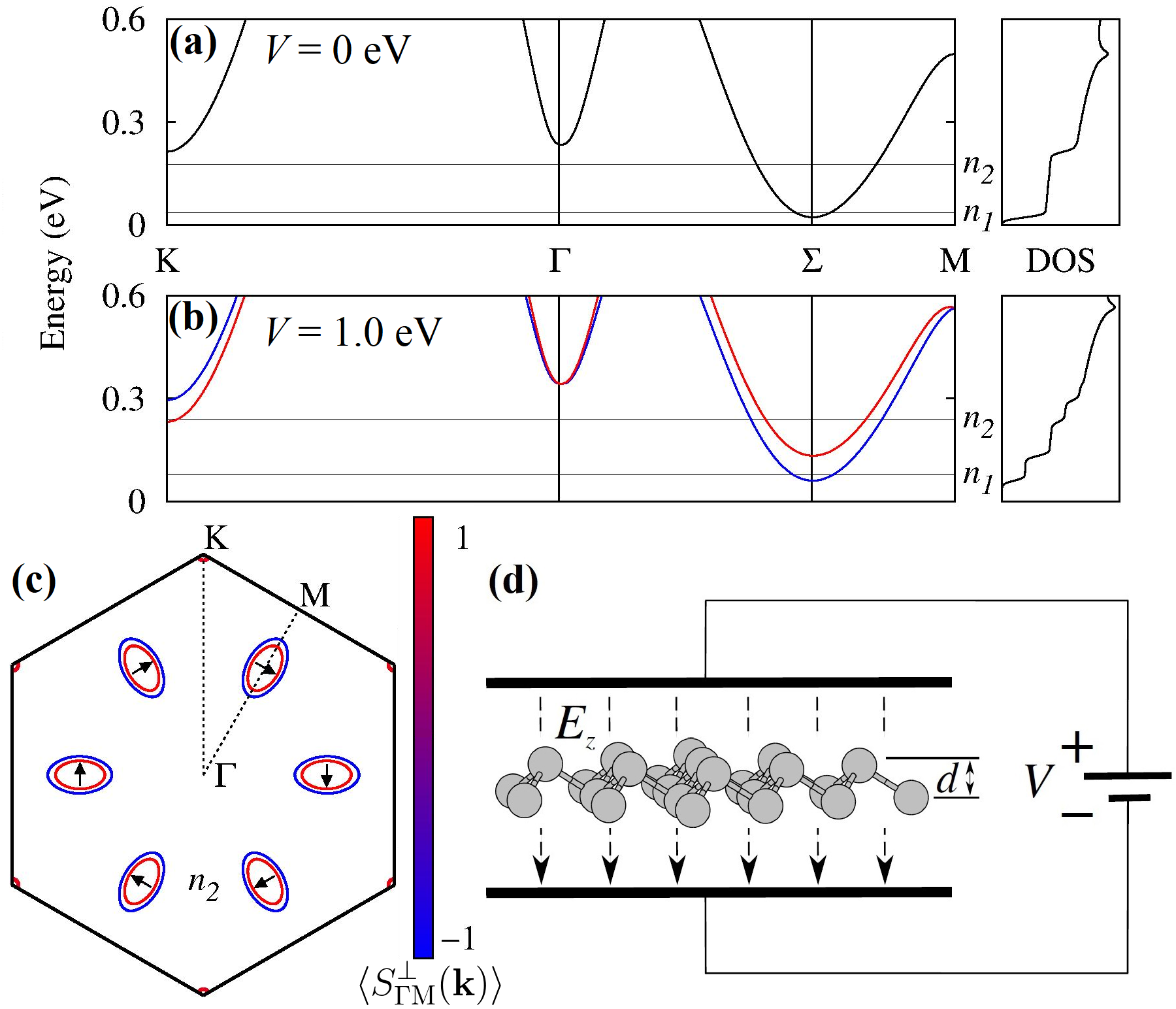
where () is the creation (annihilation) operator of electrons with spin () at orbital (), is the -component of the position operator of the orbital , is the spin-dependent matrix of hopping integrals, is bias voltage applied to the upper and lower planes of the system, and is the vertical displacement between the sublattices [Fig. 1(d)].
Fig. 1(a) shows energy dispersion and density of states (DOS) of the conduction states of SL-Sb. The conduction band minimum corresponds to a low-symmetry -point ( point group), which is located at 0.56 Å-1 from the -point along the –M direction of the Brillouin zone. Low energy dispersion at the band edge can be described by two effective masses, and , corresponding to the direction along and perpendicular to –M, respectively. This gives rise to six ellipsoidal valleys formed around the zone center. In the presence of a vertical bias (or perpendicular static electric field), the spin degeneracy is lifted as a result of inversion symmetry breaking [40]. The resulting spin splitting is shown in Fig. 1(b), which reaches 0.1 eV at the bias voltage eV. In this situation, the effective masses enhance to and for both bands. The corresponding Fermi energy contours are shown in Fig. 1(c), where projections on the opposite spin directions is shown by color. The splitting of electron states in SL-Sb is different from the Rashba splitting typical to narrow gap 2D electron gas, but rather resembles exchange splitting in the ferromagnets [41]. Indeed, the expectation value of the spin operator projected to the direction perpendicular to –M, , shows that the two states within each valley correspond to the opposite () spin projections [see Fig. 1(c)]. In contrast to ferromagnets, time reversal symmetry is preserved in biased SL-Sb, leading to zero net magnetization.
The combination of a gate-controlled band splitting and finite DOS at the Fermi energy achievable by doping opens up the possibility to tune plasmonic resonances in SL-Sb, which is of interest for practical applications. Here, we restrict ourselves to the case of electron doping only, as it represents the most interesting case. We only note that the properties of hole-doped SL-Sb can be with high accuracy described by the well-studied Rashba model [42].
To investigate optical properties of SL-Sb, we first calculate frequency-dependent dielectric matrix . To this end, we use the random phase approximation assuming no dielectric background (free-standing sample):
| (2) |
where is the long-wavelength approximation of the bare Coulomb interaction density in 2D, and is the polarizability matrix. For the purpose of our study it is sufficient to ignore local field effects related to the orbital degrees of freedom, while the effects of the spin subsystem turn out to be important. Using the definition given above, the spectrum of plasma excitations is determined by the equation , where is the damping factor, and is the plasma frequency. In the spinor basis, the polarizability can be defined as [43]:
| (3) |
where is the contribution of the th orbital with spin to the Hamiltonian eigenstate with energy , , is Fermi-Dirac occupation factor, is the chemical potential determined by the carrier concentration , and is a broadening term. In our calculations, we used K, meV, and two representative values of electron doping, and cm-2. Brillouin zone integration has been performed on a grid of 106 k-points.
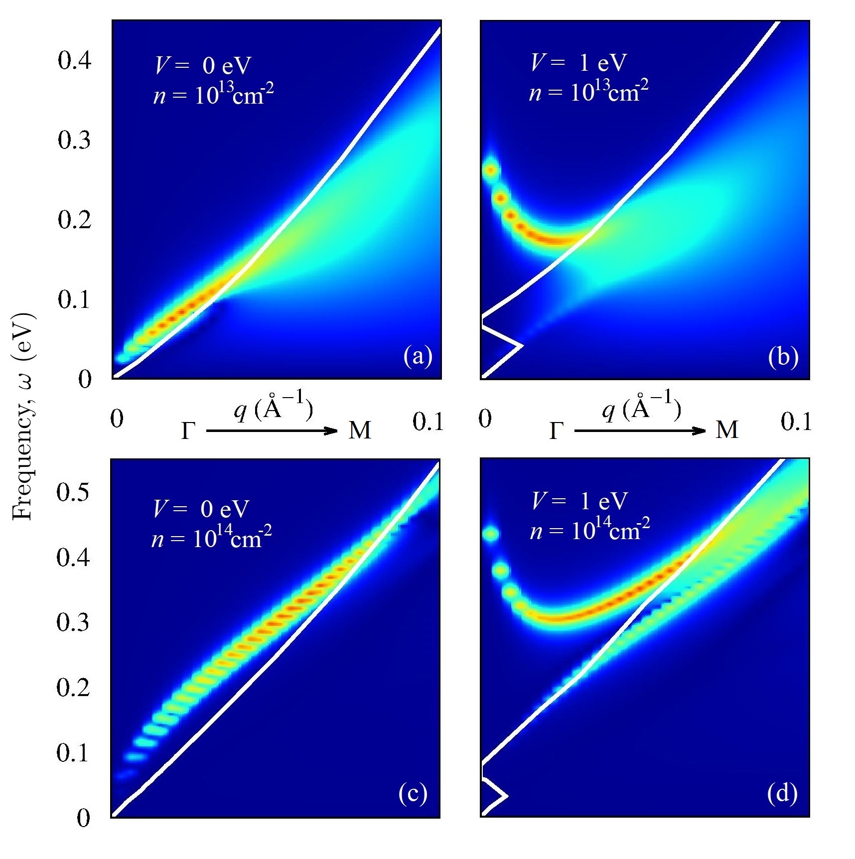
To understand the extent to which one can tune the optical properties of SL-Sb, we calculate the plasmon loss function , and study its behavior with respect to the carrier doping and external potential strength. The results are presented in Fig. 2, which also shows boundaries of the particle-hole continuum, . In the absence of external potential electron occupy the bottom of a single parabolic band with no interband transition allowed [see Fig. 1(a)]. In this situation, optical response is determined by the plasma oscillations of nonrelativistic 2D electron gas, for which one has , where and are constants, and is the Fermi energy [44]. The corresponding loss function for and cm-2 is shown in Figs. 2(a) and (c), from which one can see a “classical” plasmon dispersion at low frequencies. At the plasmon dispersion enters single-particle excitation continuum and decays into electron-hole pairs. The energy scale of phonon excitations in SL-Sb lies in the far-IR region [40], meaning the absence of phonon-plasmon resonances [45] in the relevant spectral range.
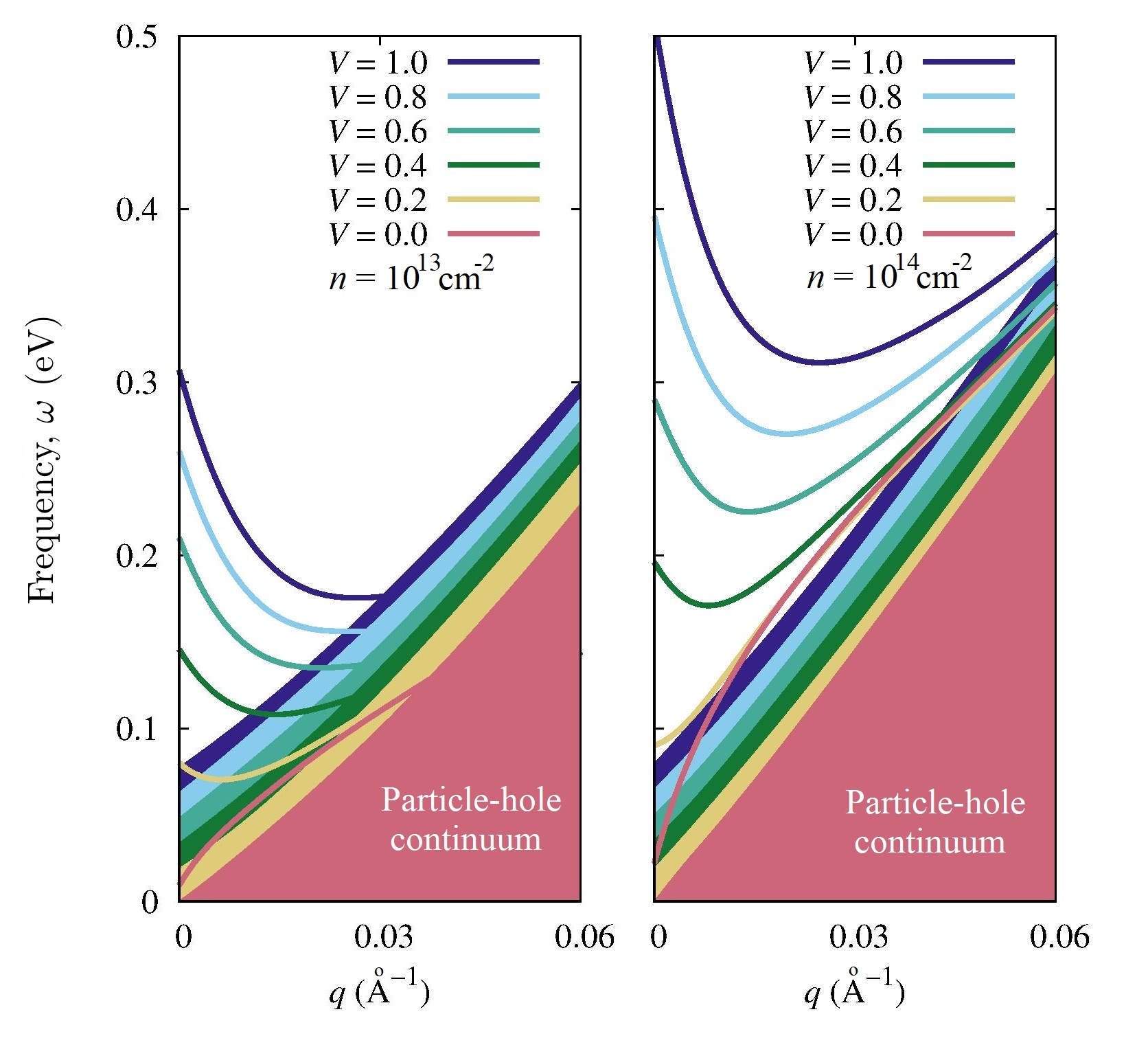
The plasmon spectrum changes drastically when we introduce external bias potential with magnitude 1 eV, see Figs. 2(b) and (d). In this case, a second (“optical”) plasmon branch appears. The new branch has large spectral weight and lies in the mid-IR region, independently of the electron concentrations considered. These excitations have a peculiar parabolic-like negative dispersion at small . Their origin is related to the SOI-mediated splitting of the conduction band [Fig. 1(b)] allowing for the interband transitions, reminiscent to that in bilayer graphene [45, 46]. The frequency of the excitations at small can be effectively tuned by gate voltage, as it is shown in Fig. 3. Depending on the level of electron doping (1013 or 1014 cm-2), one can smoothly tune from 0 to 0.3 (or 0.5) eV by applying bias voltage in the range up to 1 eV. In all cases relevant excitations lie above the Landau damping region (), indicating fully coherent plasmon modes. On the contrary, “classical” plasmon mode in biased SL-Sb falls inside the particle-hole continuum, and turns out to be essentially damped. As a consequence of the Kramers-Kronig sum rule [47], the entire spectral weight at long wavelengths is transferred to the “optical” mode. We note that further tunability toward lower frequencies can be achieved by the dielectric substrate (not considered here).
To gain further insights into the origin of plasma excitations in SL-Sb, we analyze effective dielectric functions , shown in Fig. 4 for cm-2. Without bias potential [Fig. 4(a)] one has typical behavior at large enough frequencies with . At there is another solution of the equation with . This solution is known as the “acoustic” plasmon mode corresponding to out-of-phase charge density oscillations observed in 2D materials with finite thickness, including bilayer graphene [48], transition metal dichalcogenides [49], and phosphorene [50]. Similar to the other systems, this mode is strongly damped as it lies in the particle-hole continuum. If we introduce bias potential [Fig. 4(b)], exhibits a discontinuity at , and has the characteristic shape typical to a conductor with resonant scatterers [51],
| (4) |
where denotes different scattering channels, which in our case can be associated with intraband and interband transitions. Eq. (4) allows for the existence of plasmons with negative dispersion if there is for which . As can be seen from Figs. 2(b) and (d), this condition is fulfilled in biased SL-Sb at Å-1, which coincides with the region of negative plasmon dispersion. Apart from this prominent solution, there is an overdamped plasmon mode at frequencies close to the interband resonance [Fig. 4(b)], while the “acoustic” branch turns out to be fully suppressed at large enough .
Plasmon excitations with negative dispersion is uncommon but not unique phenomenon. It was first appeared in the context of bulk Cs crystal [52], but was further observed in other materials [53, 54]. A recent study reports similar behavior in electron-doped monolayer MoS2 [55]. Negative dispersion is associated with negative group velocity, indicating negative energy flux. This phenomenon gives rise to an intriguing subfield of nanoplasmonics with a number of exotic optical effects including negative refraction index [56, 57, 58]. The fact that the corresponding frequencies in SL-Sb fall in the technologically relevant spectral range make this system prospective for further experimental studies. Plasmons in 2D systems can be accessed by a variety of methods, including electron energy-loss spectroscopy [13], IR optical measurements [15], and scanning probe microscopy [17], performed earlier for graphene. High tunability of plasmon excitations in SL-Sb offered by the strong SOI is another appealing aspect to be explored in the context of nanoplasmonic applications. To experimentally observe the peculiar character of plasmons in SL-Sb, strong electric fields on the order of 0.1–0.5 eV/Å may be required. This can be achieved, for example, by the encapsulation of SL-Sb in polar semiconductors [59], or by means of heavy alkali metal doping [60].
To conclude, we theoretically studied optoelectronic properties of SL-Sb at realistic electron concentrations by varying the applied gate voltage. In addition to the classical 2D plasmon, we find that SOI-induced spin splitting gives rise to a new lossless plasmon branch in the mid-IR region at frequencies highly sensitive to the bias voltage. Remarkably, the new excitations exhibit negative dispersion in a wide range of wavevectors. This behavior is attributed to the strong SOI and inversion symmetry breaking, as well as indicates an important role of the local field effects in the spin channel. Our findings suggest SL-Sb to be an appealing nanoplasmonic material with great gate-tunability, which paves the way for further experimental and theoretical studies in this field.
Acknowledgements.
This work was supported by the Russian Science Foundation, Grant No. 17-72-20041. Part of the research was carried out using high performance computing resources at Moscow State University [61].References
- Maier [2007] S. A. Maier, Plasmonics: Fundamentals and Applications (Springer, New York, 2007).
- Murray and Barnes [2007] W. A. Murray and W. L. Barnes, “Plasmonic Materials”, Adv. Mater. 19, 3771 (2007).
- Boriskina et al. [2013] S. V. Boriskina, H. Ghasemi, and G. Chen, “Plasmonic materials for energy: From physics to applications”, Mater. Today 16, 375 (2013).
- Kneipp et al. [1997] K. Kneipp, Y. Wang, H. Kneipp, L. T. Perelman, I. Itzkan, R. R. Dasari, and M. S. Feld, “Single molecule detection using surface-enhanced raman scattering (SERS)”, Phys. Rev. Lett. 78, 1667 (1997).
- Mayer and Hafner [2011] K. M. Mayer and J. H. Hafner, “Localized surface plasmon resonance sensors”, Chem. Rev. 111, 3828 (2011).
- Rodrigo et al. [2015] D. Rodrigo, O. Limaj, D. Janner, D. Etezadi, F. J. García de Abajo, V. Pruneri, and H. Altug, “Mid-infrared plasmonic biosensing with graphene”, Science 349, 165 (2015).
- Sorger et al. [2012] V. J. Sorger, R. F. Oulton, R.-M. Ma, and X. Zhang, “Toward integrated plasmonic circuits”, MRS Bull. 37, 728 (2012).
- Zhong et al. [2015] Y. Zhong, S. D. Malagari, T. Hamilton, and D. M. Wasserman, “Review of mid-infrared plasmonic materials”, J. Nanophotonics 9, 093791 (2015).
- Low et al. [2016] T. Low, A. Chaves, J. D. Caldwell, A. Kumar, N. X. Fang, P. Avouris, T. F. Heinz, F. Guinea, L. Martin-Moreno, and F. Koppens, “Polaritons in layered two-dimensional materials”, Nat. Mater. 16, 182 (2016).
- Li et al. [2018] Y. Li, Z. Li, C. Chi, H. Shan, L. Zhen, and Z. Fang, “Plasmonics of 2D nanomaterials: Properties and applications”, Adv. Sci. 4, 1600430 (2018).
- Pfnür et al. [2017] H. Pfnür, C. Tegenkamp, and L. Vattuone, “Plasmons in one and two dimensions”, arXiv:1701.05049 (2017).
- Agarwal et al. [2018] A. Agarwal, M. S. Vitiello, L. Viti, A. Cupolillo, and A. Politano, “Plasmonics with two-dimensional semiconductors: from basic research to technological applications”, Nanoscale 10, 8938 (2018).
- Gass et al. [2008] M. H. Gass, U. Bangert, A. L. Bleloch, P. Wang, R. R. Nair, and A. K. Geim, “Free-standing graphene at atomic resolution”, Nat. Nanotech. 3, 676 (2008).
- Koppens et al. [2011] F. H. L. Koppens, D. E. Chang, and F. J. G. de Abajo, “Graphene plasmonics: A platform for strong light–matter interactions”, Nano Lett. 11, 3370 (2011).
- Fei et al. [2011] Z. Fei, G. O. Andreev, W. Bao, L. M. Zhang, A. S. McLeod, C. Wang, Z. Zhao, G. Dominguez, M. Thiemens, M. M. Fogler, M. Tauber, A. Castro-Neto, C. N. Lau, F. Keilmann, and D. N. Basov, “Infrared Nanoscopy of Dirac Plasmons at the Graphene-SiO2 Interface”, Nano Lett. 11, 4701 (2011).
- Chen et al. [2012] J. Chen, M. Badioli, P. Alonso-González, S. Thongrattanasiri, F. Huth, J. Osmond, M. Spasenovic, A. Centeno, A. Pesquera, P. Godignon, A. Zurutuza Elorza, N. Camara, F. J. G. de Abajo, R. Hillenbrand, and F. H. L. Koppens, “Optical nano-imaging of gate-tunable graphene plasmons”, Nature 487, 77 (2012).
- Fei et al. [2012] Z. Fei, A. S. Rodin, G. O. Andreev, W. Bao, A. S. McLeod, M. Wagner, L. M. Zhang, Z. Zhao, M. Thiemens, G. Dominguez, M. M. Fogler, A. H. C. Neto, C. N. Lau, F. Keilmann, and D. N. Basov, “Gate-tuning of graphene plasmons revealed by infrared nano-imaging”, Nature 487, 82 (2012).
- Grigorenko et al. [2012] A. N. Grigorenko, M. Polini, and K. S. Novoselov, “Graphene plasmonics”, Nat. Photonics 6, 749 (2012).
- Kim et al. [2012] J. Kim, H. Son, D. J. Cho, B. Geng, W. Regan, S. Shi, K. Kim, A. Zettl, Y.-R. Shen, and F. Wang, “Electrical control of optical plasmon resonance with graphene”, Nano Lett. 12, 5598 (2012).
- Brar et al. [2013] V. W. Brar, M. S. Jang, M. Sherrott, J. J. Lopez, and H. A. Atwater, “Highly confined tunable mid-infrared plasmonics in graphene nanoresonators”, Nano Lett. 13, 2541 (2013).
- Stauber [2014] T. Stauber, “Plasmonics in Dirac systems: from graphene to topological insulators”, J. Phys.: Cond. Matter 26, 123201 (2014).
- Rodrigo et al. [2017] D. Rodrigo, A. Tittl, O. Limaj, F. J. G. d. Abajo, V. Pruneri, and H. Altug, “Double-layer graphene for enhanced tunable infrared plasmonics”, Light Sci. Appl. 6, 16277 (2017).
- Yao et al. [2018] B. Yao, Y. Liu, S.-W. Huang, C. Choi, Z. Xie, J. Flor Flores, Y. Wu, M. Yu, D.-L. Kwong, Y. Huang, Y. Rao, X. Duan, and C. W. Wong, “Broadband gate-tunable terahertz plasmons in graphene heterostructures”, Nat. Photonics 12, 22 (2018).
- Scholz et al. [2013] A. Scholz, T. Stauber, and J. Schliemann, “Plasmons and screening in a monolayer of MoS2”, Phys. Rev. B 88, 035135 (2013).
- Wang et al. [2015] Y. Wang, J. Z. Ou, A. F. Chrimes, B. J. Carey, T. Daeneke, M. M. Y. A. Alsaif, M. Mortazavi, S. Zhuiykov, N. Medhekar, M. Bhaskaran, J. R. Friend, M. S. Strano, and K. Kalantar-Zadeh, “Plasmon resonances of highly doped two-dimensional MoS2”, Nano Lett. 15, 883 (2015).
- Mishra et al. [2016] A. K. Mishra, S. K. Mishra, and R. K. Verma, “Graphene and beyond graphene MoS2: A new window in surface-plasmon-resonance-based fiber optic sensing”, J. Phys. Chem. C 120, 2893 (2016).
- Low et al. [2014a] T. Low, R. Roldán, H. Wang, F. Xia, P. Avouris, L. M. Moreno, and F. Guinea, “Plasmons and screening in monolayer and multilayer black phosphorus”, Phys. Rev. Lett. 113, 106802 (2014a).
- Correas-Serrano et al. [2016] D. Correas-Serrano, J. S. Gomez-Diaz, A. A. Melcon, and A. Alù, “Black phosphorus plasmonics: anisotropic elliptical propagation and nonlocality-induced canalization”, J. Opt. 18, 104006 (2016).
- Liu and Aydin [2016] Z. Liu and K. Aydin, “Localized Surface Plasmons in Nanostructured Monolayer Black Phosphorus”, Nano Lett. 16, 3457 (2016).
- Nemilentsau et al. [2016] A. Nemilentsau, T. Low, and G. Hanson, “Anisotropic 2D materials for tunable hyperbolic plasmonics”, Phys. Rev. Lett. 116, 066804 (2016).
- Gong et al. [2017] C. Gong, L. Li, Z. Li, H. Ji, A. Stern, Y. Xia, T. Cao, W. Bao, C. Wang, Y. Wang, Z. Q. Qiu, R. J. Cava, S. G. Louie, J. Xia, and X. Zhang, “Discovery of intrinsic ferromagnetism in two-dimensional van der Waals crystals”, Nature 546, 265 (2017).
- Huang et al. [2017] B. Huang, G. Clark, E. Navarro-Moratalla, D. R. Klein, R. Cheng, K. L. Seyler, D. Zhong, E. Schmidgall, M. A. McGuire, D. H. Cobden, W. Yao, D. Xiao, P. Jarillo-Herrero, and X. Xu, “Layer-dependent ferromagnetism in a van der Waals crystal down to the monolayer limit”, Nature 546, 270 (2017).
- Armelles et al. [2013] G. Armelles, A. Cebollada, A. García-Martín, and M. U. González, “Magnetoplasmonics: Combining Magnetic and Plasmonic Functionalities”, Adv. Opt. Mater. 1, 10 (2013).
- Ares et al. [2016] P. Ares, F. Aguilar-Galindo, D. Rodríguez-San-Miguel, D. A. Aldave, S. Díaz-Tendero, M. Alcamí, F. Martín, J. Gómez-Herrero, and F. Zamora, “Mechanical isolation of highly stable antimonene under ambient conditions”, Adv. Mater. 28, 6332 (2016).
- Wu et al. [2017] X. Wu, Y. Shao, H. Liu, Z. Feng, Y. L. Wang, J. T. Sun, C. Liu, J. O. Wang, Z. L. Liu, S. Y. Zhu, Y. Q. Wang, S. X. Du, Y. G. Shi, K. Ibrahim, and H. J. Gao, “Epitaxial Growth and Air-Stability of Monolayer Antimonene on PdTe2”, Adv. Mater. 29, 1605407 (2017).
- Pizzi et al. [2016] G. Pizzi, M. Gibertini, E. Dib, N. Marzari, G. Iannaccone, and G. Fiori, “Performance of arsenene and antimonene double-gate mosfets from first principles”, Nat. Commun. 7, 12585 (2016).
- Zhao et al. [2015] M. Zhao, X. Zhang, and L. Li, “Strain-driven band inversion and topological aspects in antimonene”, Sci. Rep. 5, 16108 (2015).
- Rudenko et al. [2017] A. N. Rudenko, M. I. Katsnelson, and R. Roldán, “Electronic properties of single-layer antimony: Tight-binding model, spin-orbit coupling, and the strength of effective coulomb interactions”, Phys. Rev. B 95, 081407 (2017).
- Ares et al. [2017] P. Ares, J. J. Palacios, G. Abellán, J. Gómez-Herrero, and F. Zamora, “Recent progress on antimonene: A new bidimensional material”, Adv. Mater. 30, 1703771 (2017).
- Lugovskoi et al. [2018] A. V. Lugovskoi, M. I. Katsnelson, and A. N. Rudenko, “Electron-phonon properties and superconductivity of doped antimonene”, arXiv:1806.08203 (2018).
- Molenkamp et al. [2001] L. W. Molenkamp, G. Schmidt, and G. E. W. Bauer, “Rashba hamiltonian and electron transport”, Phys. Rev. B 64, 121202 (2001).
- Wang [2017] X. F. Wang, “Plasmon spectrum of two-dimensional electron systems with Rashba spin-orbit interaction”, Phys. Rev. B 72, 085317 (2017).
- Graf and Vogl [1995] M. Graf and P. Vogl, “Electromagnetic fields and dielectric response in empirical tight-binding theory”, Phys. Rev. B 51, 4940 (1995).
- Stern [1967] F. Stern, “Polarizability of a two-dimensional electron gas”, Phys. Rev. Lett. 18, 546 (1967).
- Low et al. [2014b] T. Low, F. Guinea, H. Yan, F. Xia, and P. Avouris, “Novel midinfrared plasmonic properties of bilayer graphene”, Phys. Rev. Lett. 112, 116801 (2014b).
- Gamayun [2011] O. V. Gamayun, “Dynamical screening in bilayer graphene”, Phys. Rev. B 84, 085112 (2011).
- Tanuma et al. [1993] S. Tanuma, C. J. Powell, and D. R. Penn, “Use of sum rules on the energy-loss function for the evaluation of experimental optical data”, J. Electron. Spectrosc. Relat. Phenom. 62, 95 (1993).
- Hwang and Das Sarma [2007] E. H. Hwang and S. Das Sarma, “Dielectric function, screening, and plasmons in two-dimensional graphene”, Phys. Rev. B 75, 205418 (2007).
- Andersen and Thygesen [2013] K. Andersen and K. S. Thygesen, “Plasmons in metallic monolayer and bilayer transition metal dichalcogenides”, Phys. Rev. B 88, 155128 (2013).
- Prishchenko et al. [2017] D. A. Prishchenko, V. G. Mazurenko, M. I. Katsnelson, and A. N. Rudenko, “Coulomb interactions and screening effects in few-layer black phosphorus: a tight-binding consideration beyond the long-wavelength limit”, 2D Mater. 4, 025064 (2017).
- Marder [2010] M. P. Marder, Condensed Matter Physics, 2nd ed. (John Wiley & Sons, Hoboken, New Jersey, 2010).
- vom Felde et al. [1989] A. vom Felde, J. Sprösser-Prou, and J. Fink, “Valence-electron excitations in the alkali metals”, Phys. Rev. B 40, 10181 (1989).
- Schuster et al. [2009] R. Schuster, R. Kraus, M. Knupfer, H. Berger, and B. Büchner, “Negative plasmon dispersion in the transition-metal dichalcogenide 2H-TaSe2”, Phys. Rev. B 79, 045134 (2009).
- van Wezel et al. [2011] J. van Wezel, R. Schuster, A. König, M. Knupfer, J. van den Brink, H. Berger, and B. Büchner, “Effect of charge order on the plasmon dispersion in transition-metal dichalcogenides”, Phys. Rev. Lett. 107, 176404 (2011).
- Tao et al. [2018] Z. H. Tao, H. M. Dong, Y. F. Duan, and F. Huang, “Novel Plasmonic Modes of Monolayer MoS2 in the Presence of Spin-Orbit Interactions”, Preprints , 2018070234 (2018).
- Agranovich and Gartstein [2006] V. M. Agranovich and Y. N. Gartstein, “Spatial dispersion and negative refraction of light”, Phys.-Usp. 49, 1029 (2006).
- Feigenbaum et al. [2009] E. Feigenbaum, N. Kaminski, and M. Orenstein, “Negative dispersion: a backward wave or fast light? Nanoplasmonic examples”, Opt. Express 17, 18934 (2009).
- Compaijen et al. [2015] P. J. Compaijen, V. A. Malyshev, and J. Knoester, “Engineering plasmon dispersion relations: hybrid nanoparticle chain-substrate plasmon polaritons”, Opt. Express 23, 2280 (2015).
- Zhang et al. [2013] D. Zhang, W. Lou, M. Miao, S.-C. Zhang, and K. Chang, “Interface-Induced Topological Insulator Transition in GaAs/Ge/GaAs Quantum Wells”, Phys. Rev. Lett. 111, 156402 (2013).
- Kim et al. [2015] J. Kim, S. S. Baik, S. H. Ryu, Y. Sohn, S. Park, B.-G. Park, J. Denlinger, Y. Yi, H. J. Choi, and K. S. Kim, “Observation of tunable band gap and anisotropic Dirac semimetal state in black phosphorus”, Science 349, 723 (2015).
- Sadovnichy et al. [2013] V. Sadovnichy, A. Tikhonravov, V. Voevodin, and V. Opanasenko, “Lomonosov: Supercomputing at Moscow State University”, in Contemporary High Performance Computing: From Petascale toward Exascale, edited by J. S. Vetter (CRC Press, Boca Raton, 2013) pp. 283–307.