Effect of multiband transport on charge carrier density fluctuations at the LaAlO3/SrTiO3 interface
Abstract
Multiband transport in superconductors is interesting both from an academic as well as an application point of view. It has been postulated that interband scattering can significantly affect the carrier dynamics in these materials. In this article we present a detailed study of the electrical transport properties of the high-mobility two-dimensional electron gas residing at the interface of LaAlO3/SrTiO3, a prototypical multi-band superconductor. We show, through careful measurements of the gate dependence of the magnetoresistance and resistance fluctuations at ultra-low temperatures, that transport in the superconducting regime of this system has contributions from two bands which host carriers of very different characters. We identify a gate-voltage tunable Lifshitz transition in the system and show that the resistance fluctuations have strikingly different features on either side of it. At low carrier densities, resistance noise is dominated by number-density fluctuations arising from trapping-detrapping of charge carriers from defects in the underlying SrTiO3 substrate, characteristic of a single-band semiconductor. Above the Lifshitz transition, the noise presumably originates from inter-band scattering. Our work highlights the importance of inter-band scattering processes in determining the transport properties of low-dimensional systems and projects resistance fluctuation spectroscopy as a viable technique for probing the charge carrier dynamics across a Lifshitz transition.
Multiband transport in superconductors is a very active field of research. It is believed that the enhancement of the superconducting transition temperature seen in many superconductors such as MgB2 Iavarone et al. (2002), H3S Jarlborg and Bianconi (2016) and FeSe Lin et al. (2016) is intricately related to a multiband Lifshitz transition. Multiple condensates in these superconducting material can interfere leading to effects not seen in single-band superconductors. It has been postulated that inter-band scattering can significantly affect the carrier dynamics in these materials. Deconvoluting the contributions of the Cooper pairs residing in different bands to electrical transport properties has proven to be quite difficult. In the case of theoretical investigations, the complication arises partly from the fact that these superconductors cannot be described by the phenomenological Ginzburg-Landau picture - rather by the Usadel equations which are theoretically more intractable. Thus, despite research for over a decade, there exists many open questions regarding the effect of the presence of multiple types of carriers and their interactions on superconductivity.
We approach this problem by studying the carrier dynamics in a well known two-dimensional superconductor at temperatures slightly above the superconducting . Oxide heterostructure as for example, the interface between (001) oriented SrTiO3 and LaAlO3 [hereafter referred to as LaAlO3/SrTiO3] has emerged as one of the most interesting material in condensed matter physics Ohtomo and Hwang (2004). Beyond a certain critical thickness of the LaAlO3 layer, a conducting quasi-two dimensional electron gas (q-2DEG) appears at the interface Thiel et al. (2006). Depending on the temperature and charge carrier density , this q-2DEG can show a broad range of phenomena including superconductivity, ferromagnetism and Rashba spin-orbit coupling Sulpizio et al. (2014); Hwang et al. (2012) (SOC). Despite intense research over the past decade Sulpizio et al. (2014), the origin of the charge carriers at the interface remains an open question. It is widely believed that the charge carriers appear at the polar/non-polar interface due to electron transfer from the topmost LaAlO3 layer to the levels of -orbitals of Ti at the interface Mannhart et al. (2008). The three-fold degeneracy of levels found in bulk SrTiO3 is lifted in the case of LaAlO3/SrTiO3 by quantum confinement induced in the z-direction. This causes the orbital to have a lower energy (by about 50 meV) than the orbital Joshua et al. (2012). Thus, beyond a certain value of the sheet charge carrier density the system can undergo a Lifshitz transition from a single band occupancy to a multiple band occupancy. Across the Lifshitz transition, the electrical transport characteristics of the q-2DEG changes quite significantly: the Hall coefficient becomes a non-linear function of the magnetic field Joshua et al. (2012); Smink et al. (2017), a novel transient superconducting state appears Daptary et al. (2017) and the longitudinal Hall resistance becomes anomalous Joshua et al. (2013). The value of has been experimentally found to lie in the range of 1013cm-2 Joshua et al. (2012); Eerkes et al. (2013); Hurand et al. (2015); Smink et al. (2017). Evidence of multiband transport has been seen in other experiments as well as, e.g., in optical transmission spectroscopy Seo et al. (2009) and thermal transport measurements Lerer et al. (2011).
Resistance fluctuation measurements are a well established technique for studying charge carrier dynamics in condensed matter systems. In a previous publication we have reported the existence of large non-Gaussian resistance fluctuations around the superconducting transition temperature in LaAlO3/SrTiO3 Daptary et al. (2016). These fluctuations were found to arise from the percolative transition of a Josephson-coupled superconducting networks. In this article, we concentrate on a temperature range slightly above the superconducting . Previous studies have shown that at around , superconductivity is a hidden order which manifested itself as a transient phase under a large perpendicular time varying magnetic field at charge carrier densities Daptary et al. (2017). There have also been previous reports of the observation of pseudogap Richter et al. (2013) over this temperature range implying the presence of superconducting fluctuations without global phase coherence. These observations have been attributed to the fact that multiple bands might contribute to the transport in this system. This prompted us to study electrical transport and noise over this temperature regime and to look for possible signatures of effect of multiband transport. In this article, we present results of the measurements of resistance fluctuations (noise) at as the chemical potential is tuned across the Lifshitz transition. We observe a drastic change in the electrical transport properties as the system undergoes the transition. We attribute these changes to the difference between the nature of scattering of the charge carriers in the different bands.
.
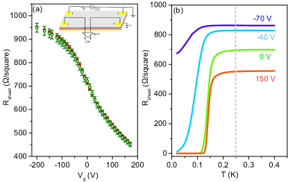
Our measurements were performed on samples with ten unit cells (u.c.) of LaAlO3 grown by pulsed laser deposition on TiO2 terminated (001) SrTiO3 single crystal substrates of thickness 0.5 mm (for details of sample preparation see Ref. Kumar et al. (2015)). The charge carrier density at the interface was controlled by a back-gate voltage with the SrTiO3 acting as the dielectric material. Electrical contact pads were prepared on top of the LaAlO3 substrate by thermal evaporation of 5 nm Cr followed by 70 nm of Au. These contact pads were ultrasonically wire bonded to the measurement chip-carrier - a process which is known to breakdown the 10 uc. of LaAlO3 and give Ohmic contacts to the underlying electron gas Caviglia et al. (2008); Joshua et al. (2012); Shalom et al. (2010). The carrier density at the interface was modulated using back gate voltage . A schematic of the device structure is shown in the inset of Fig. 1(a) along with the electrical connections. The temperature dependence of the resistance was measured in a cryo-free dilution refrigerator equipped with a 16 T magnetic field and the noise measurements were performed at 245 mK in a He-3 refrigerator (base temperature of the refrigerator) with a temperature stability of better than 0.5 mK. Measurements were performed on two different devices. In this article we concentrate on the data from one particular device, and the data from the other device was qualitatively similar.
In Fig. 1(a) we plot the sheet resistance as a function of back gate voltages at 245 mK. The data have been taken for decreasing gate voltages. We found that upon initial cool down, the resistance versus curves were always hysteretic and non-reproducible. Repeated sweeps between the maximum and the minimum values of at the lowest temperature stabilized the resistance values and the curves became reproducible while still remaining hysteretic. This is a common feature of this system and has been reported by several groups Biscaras et al. (2014); Rössle et al. (2013). We have taken care to always perform the noise and magnetoresistance measurements only for decreasing gate voltages, going only in one direction of sweep – from +200 V to -200 V. The monotonic decrease in with increasing seen in the plot has been reported previously by several groups Caviglia et al. (2008); Dikin et al. (2011); Daptary et al. (2017) and confirms that the charge carriers are electrons. In Fig. 1(b) we plot the sheet resistance as a function of at few representative values of . With changing , both the superconducting transition temperature and normal state resistance change. The subsequent measurements reported in this article were all performed at =245 mK ( 1.8, being the mean field superconducting transition temperature at =0 V), marked by a vertical dashed line in Fig. 1(b).
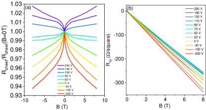
In Fig. 2(b), we plot the Hall resistance at a few representative values of . We notice that above a characteristic value of the gate voltage, which we denote as [100 V for this particular device], both the Hall resistance and the magnetoresistance change in character. Below , is linear in magnetic field , and its slope decreases with increasing signifying an increase in electron doping of the system. over this field range shows a negative magnetoresistance (see Fig. 2(a)). Above , becomes non-linear in developing a distinct kink whereas has a positive magnetoresistance. This change from a negative magnetoresistance to a positive magnetoresistance around a certain value of has been observed before in LaAlO3/SrTiO3 heterostructures and has been interpreted to be due to a transition from weak localization to weak anti-localization mediated by the large Rashba SOC present in this system Caviglia et al. (2010a). At low values of (single-band regime), quantum corrections to the Drude magnetoconductivity is ascribable to weak localization. At the single- to multiband crossover, the large enhancement in the density of states at the Fermi energy leads to an increase in the strength of the Rashba spin-orbit coupling. This causes the spin relaxation time to become much smaller than the inelastic scattering time leading to the appearance of weak anti-localization and consequently positive magnetoresistance.
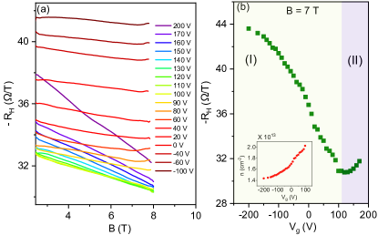
In Fig. 3(a) we plot the Hall coefficient (=) as a function of the magnetic field at different values of . We find that for V, is almost independent of and decreases monotonically with an increase in . For V, depends on magnetic field and increases with an increase in . This value of V, where there is a quantitative change in the character of Hall resistance, we refer to as . The non-linear Hall resistance observed for can have multiple possible origins – the ones most relevant to this system being Shubnikov-de Haas oscillations (SdH), anomalous Hall effect (AHE) due to magnetization induced by the external magnetic field Shalom et al. (2010); Seri and Klein (2009) or the AHE due to conduction through multiple bands Kim et al. (2010). We do not observe SdH oscillations in our devices, presumably due to the low mobility of our samples Caviglia et al. (2010b). The main signature of the AHE due to B-field induced magnetization is saturation of the Hall resistance at high fields Lee et al. (2011). The fact that we do not see such saturation at high fields rules out this scenario. We can also rule out the AHE due to magnetic moments by noting that the effect of ferromagnetism in this system is strongest at low doping levels whereas the observed non-linearity appears at high doping levels. This leaves us to consider the AHE induced by multiband transport as the most plausible origin of the non-linear Hall observed by us Joshua et al. (2012); Bell et al. (2009); Kim et al. (2010).
In Fig. 3(b) we plot as a function of . In the plot we define two regions: (I) (light yellow shaded region) where decreases monotonically with increasing and (II) (light gray shaded region) where increases with increasing . In region I () the hall resistance is linear in and consequently the charge carrier density can be extracted using the form . The value of (shown in the inset of Fig. 3(b)) increases monotonically with increasing over this range of gate voltages and matches well with that estimated by taking into account the dielectric constant of SrTiO3 Daptary et al. (2017). These observations affirm that over this doping range, transport is dominated by a single-type of carrier. Above , where the non-linearity in Hall resistance sets in, it becomes essential to consider the contributions of multiple-types of charge carriers.
Given the fact that the q-2DEG is spread over multiple layers of Ti atoms, each presumably having different band configuration, it is difficult to develop a model that can describe quantitatively the observed Hall signal for . Nevertheless, as a first approximation, we analyze our Hall data using the two-carrier model following the formalism developed in Ref. Joshua et al. (2012); Bansal et al. (2012); Lerer et al. (2011); Kim et al. (2010):
| (1) |
with the constraint (). This model effectively considers the contribution from only one Ti layer or alternatively assumes that the electronic band structure and the band occupation in all the layers are the same. Here (, ) are the carrier density and the mobility of electrons whereas (, ) are the corresponding quantities for the electrons. In Fig. 1(a) we show a plot of the dependence of calculated using the extracted values of , , and . We find that the calculated resistance values match with the measured resistance to within 2%.
The critical carrier density (corresponding to ), at which the system undergoes a transition from a single-band-type to multiple-bands-type transport is 1013cm-2 for this device - close to the number density range where the system is postulated to undergo a Lifsitz transition Joshua et al. (2012); Smink et al. (2017). The Hall measurements thus indicate that, as discussed earlier, at low charge carrier densities, the itinerant electrons occupy a single orbital. With increasing charge carrier density, the system undergoes a Lifstitz transition and the higher energy bands (predicted to be a mixture of bare bands modified by atomic spin-energy coupling Joshua et al. (2012)) begin to be occupied.
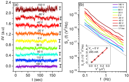
To probe the dynamics of charge carriers across this transition, we measured the resistance fluctuations in the sample at different . The measurements were performed using a digital signal processing based ac technique Ghosh et al. (2004) which allows simultaneous measurement of the background noise (Nyquist noise+instrumentation noise) as well as the bias-dependent noise originating due to resistance fluctuations of the sample. A low noise pre-amplifier (SR552) was used to couple the sample to a lock-in-amplifier (LIA). The carrier frequency of the LIA (we used = 228 Hz) was chosen lie in a region where the noise from the detection electronics was a minimum. The demodulated output signal of the LIA is digitized by a high-speed 16-bit analog-to-digital card and forms the time series of voltage fluctuations . The voltage time series, consisting of 5 106 data points for each , was digitally decimated and filtered to eliminate the 50 Hz line frequency. The power spectral density (PSD) of voltage fluctuations, was obtained from this filtered time-series of voltage fluctuations by fast Fourier-transform over the spectral range of 90 mHz–8 Hz. The measurement system was calibrated down to spectral power V2/Hz by measuring the Johnson-Nyquist noise of a standard resistor. Typical time series of voltage fluctuations at several different values of are shown in Fig. 4(a). The corresponding are plotted in Fig. 4(b). At all gate voltages, with . depended quadratically on the voltage across the sample (see Fig. 4(b) inset) indicating that the noise was generated from the resistance fluctuations of the sample.
To compare the noise level of LaAlO3/SrTiO3 with other low-dimensional disordered superconductors, we calculated the Hooge parameter defined as ; being the total number of charge carriers in the system. The value of extracted at V and =245 mK is . This value is significantly lower than what is typically seen in other low-dimensional disordered superconductors, e.g. NbN thin films () Koushik et al. (2013).
.
A quantitative estimate of the dependence of the resistance fluctuations on can be obtained by evaluating the relative variance of resistance fluctuations defined as:
| (2) |
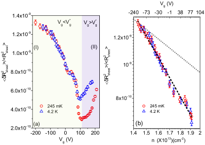
where is the variance of the sheet resistance. In Fig. 5(a), we plot as a function of at 245 mK and 4.2 K. In region I (), the noise decreases monotonically with increasing until . On the other hand, for , we find that the noise increased with increasing .
What can cause this dependence of the measured noise on , or equivalently, on the charge carrier density? Resistance noise in a system can arise either due to fluctuations in the mobility or in the charge-carrier number density:
| (3) |
where and are variance in mobility and carrier density respectively. In a metallic system, the predominant contribution to noise comes from mobility fluctuations, in which case the noise scales as Hooge (1994). In semiconductors, on the other hand the dominant source of noise is fluctuation in the charge carrier number density which leads to Jayaraman and Sodini (1989). In Fig. 5(b), we show a plot of noise as a function of for . We find that the data are well fitted with , with establishing that the resistance fluctuations over this range of doping is dominated by carrier density fluctuations. A physical mechanism of this process was proposed by McWhorter Jayaraman and Sodini (1989), who showed that a major contribution to the resistance noise in semiconductors is from the modulation of carrier density in the conducting channel due to trapping-detrapping from defect states. This requires the presence of an activated random process that can promote carriers from defect states in substrates or the bulk of the material to the conducting channel. The trap density extracted from the noise data using the McWhorter model Jayaraman and Sodini (1989) is cm-2eV-1 which matches well with prior reports of trap-densities measured in SrTiO3 Yadav and Ghosh (2016). A condition for the validity of the inverse square scaling of the noise with is that the charge carrier density must be higher than the density of traps Vandamme and Hooge (2005), a condition that is satisfied in our system.
The noise for has an upturn with increasing carrier density. Such an increase in noise with increase in is rarely seen. There have been reports of increase in resistance noise in superconducting systems as multiple bands become accessible to the system with varying temperature or bias Barone et al. (2011, 2014, 2013). It has been proposed that a possible reason for this can be an increase in the available number of scattering channels at the transition from single-band to multiband transport. In the absence of a theoretical model which quantitatively explains this behaviour, we leave a detailed explanation of the origin of the excess noise in this regime to future endeavors.
To summarize, we have studied in detail the carrier density dependence of resistance fluctuations in high quality LaAlO3/SrTiO3 heterostructures at temperatures slightly above the superconducting transition temperature. From magnetoreistance measurements we identify the critical number density at which the system undergoes Lifshitz transition from a single-band to a multiband transport. For , the measured noise arises due to fluctuations in the charge carrier density in the 2DEG. For , we propose that the observed increase in noise with carrier density could be a manifestation of scattering of carriers between different available transport channels. Our results emphasize the importance of inter-band scattering processes in systems which support carriers in multiple bands.
The authors thank R. C. Budhani for providing the samples. A.B. acknowledges funding from SERB, DST, Government of India.
References
- Iavarone et al. (2002) M. Iavarone, G. Karapetrov, A. Koshelev, W. Kwok, G. Crabtree, D. Hinks, W. Kang, E.-M. Choi, H. J. Kim, H.-J. Kim, et al., Physical review letters 89, 187002 (2002).
- Jarlborg and Bianconi (2016) T. Jarlborg and A. Bianconi, Scientific reports 6 (2016).
- Lin et al. (2016) H. Lin, Y. Li, Q. Deng, J. Xing, J. Liu, X. Zhu, H. Yang, and H.-H. Wen, Physical Review B 93, 144505 (2016).
- Ohtomo and Hwang (2004) A. Ohtomo and H. Hwang, Nature 427, 423 (2004).
- Thiel et al. (2006) S. Thiel, G. Hammerl, A. Schmehl, C. Schneider, and J. Mannhart, Science 313, 1942 (2006).
- Sulpizio et al. (2014) J. A. Sulpizio, S. Ilani, P. Irvin, and J. Levy, Annual Review of Materials Research 44, 117 (2014).
- Hwang et al. (2012) H. Y. Hwang, Y. Iwasa, M. Kawasaki, B. Keimer, N. Nagaosa, and Y. Tokura, Nature materials 11, 103 (2012).
- Mannhart et al. (2008) J. Mannhart, D. H. Blank, H. Hwang, A. Millis, and J.-M. Triscone, MRS bulletin 33, 1027 (2008).
- Joshua et al. (2012) A. Joshua, S. Pecker, J. Ruhman, E. Altman, and S. Ilani, Nature communications 3, 1129 (2012).
- Smink et al. (2017) A. Smink, J. de Boer, M. Stehno, A. Brinkman, W. van der Wiel, and H. Hilgenkamp, Physical Review Letters 118, 106401 (2017).
- Daptary et al. (2017) G. N. Daptary, S. Kumar, A. Bid, P. Kumar, A. Dogra, R. Budhani, D. Kumar, N. Mohanta, and A. Taraphder, Physical Review B 95, 174502 (2017).
- Joshua et al. (2013) A. Joshua, J. Ruhman, S. Pecker, E. Altman, and S. Ilani, Proceedings of the National Academy of Sciences 110, 9633 (2013).
- Eerkes et al. (2013) P. Eerkes, W. G. van der Wiel, and H. Hilgenkamp, Applied physics letters 103, 201603 (2013).
- Hurand et al. (2015) S. Hurand, A. Jouan, C. Feuillet-Palma, G. Singh, J. Biscaras, E. Lesne, N. Reyren, A. Barthélémy, M. Bibes, J. Villegas, et al., Scientific reports 5, 12751 (2015).
- Seo et al. (2009) S. S. A. Seo, Z. Marton, W. Choi, G. Hassink, D. H. Blank, H. Y. Hwang, T. W. Noh, T. Egami, and H. N. Lee, Applied physics letters 95, 082107 (2009).
- Lerer et al. (2011) S. Lerer, M. B. Shalom, G. Deutscher, and Y. Dagan, Physical Review B 84, 075423 (2011).
- Daptary et al. (2016) G. N. Daptary, S. Kumar, P. Kumar, A. Dogra, N. Mohanta, A. Taraphder, and A. Bid, Physical Review B 94, 085104 (2016).
- Richter et al. (2013) C. Richter, H. Boschker, W. Dietsche, E. Fillis-Tsirakis, R. Jany, F. Loder, L. Kourkoutis, D. Muller, J. Kirtley, C. Schneider, et al., Nature 502, 528 (2013).
- Kumar et al. (2015) P. Kumar, A. Dogra, P. Bhadauria, A. Gupta, K. Maurya, and R. Budhani, Journal of Physics: Condensed Matter 27, 125007 (2015).
- Caviglia et al. (2008) A. Caviglia, S. Gariglio, N. Reyren, D. Jaccard, T. Schneider, M. Gabay, S. Thiel, G. Hammerl, J. Mannhart, and J.-M. Triscone, Nature 456, 624 (2008).
- Shalom et al. (2010) M. B. Shalom, M. Sachs, D. Rakhmilevitch, A. Palevski, and Y. Dagan, Physical review letters 104, 126802 (2010).
- Biscaras et al. (2014) J. Biscaras, S. Hurand, C. Feuillet-Palma, A. Rastogi, R. Budhani, N. Reyren, E. Lesne, J. Lesueur, and N. Bergeal, Scientific reports 4, 6788 (2014).
- Rössle et al. (2013) M. Rössle, K. W. Kim, A. Dubroka, P. Marsik, C. N. Wang, R. Jany, C. Richter, J. Mannhart, C. Schneider, A. Frano, et al., Physical review letters 110, 136805 (2013).
- Dikin et al. (2011) D. Dikin, M. Mehta, C. Bark, C. Folkman, C. Eom, and V. Chandrasekhar, Physical Review Letters 107, 056802 (2011).
- Caviglia et al. (2010a) A. Caviglia, M. Gabay, S. Gariglio, N. Reyren, C. Cancellieri, and J.-M. Triscone, Physical review letters 104, 126803 (2010a).
- Seri and Klein (2009) S. Seri and L. Klein, Phys. Rev. B 80, 180410 (2009).
- Kim et al. (2010) J. S. Kim, S. S. A. Seo, M. F. Chisholm, R. K. Kremer, H.-U. Habermeier, B. Keimer, and H. N. Lee, Phys. Rev. B 82, 201407 (2010).
- Caviglia et al. (2010b) A. Caviglia, S. Gariglio, C. Cancellieri, B. Sacepe, A. Fete, N. Reyren, M. Gabay, A. Morpurgo, and J.-M. Triscone, Physical review letters 105, 236802 (2010b).
- Lee et al. (2011) Y. Lee, C. Clement, J. Hellerstedt, J. Kinney, L. Kinnischtzke, X. Leng, S. Snyder, and A. Goldman, Physical Review Letters 106, 136809 (2011).
- Bell et al. (2009) C. Bell, S. Harashima, Y. Kozuka, M. Kim, B. G. Kim, Y. Hikita, and H. Y. Hwang, Phys. Rev. Lett. 103, 226802 (2009).
- Bansal et al. (2012) N. Bansal, Y. S. Kim, M. Brahlek, E. Edrey, and S. Oh, Physical review letters 109, 116804 (2012).
- Ghosh et al. (2004) A. Ghosh, S. Kar, A. Bid, and A. Raychaudhuri, arXiv preprint cond-mat/0402130 (2004).
- Koushik et al. (2013) R. Koushik, S. Kumar, K. R. Amin, M. Mondal, J. Jesudasan, A. Bid, P. Raychaudhuri, and A. Ghosh, Physical review letters 111, 197001 (2013).
- Hooge (1994) F. Hooge, IEEE Transactions on Electron Devices 41, 1926 (1994).
- Jayaraman and Sodini (1989) R. Jayaraman and C. G. Sodini, IEEE Transactions on Electron Devices 36, 1773 (1989).
- Yadav and Ghosh (2016) S. Yadav and S. Ghosh, ACS applied materials & interfaces 8, 10436 (2016).
- Vandamme and Hooge (2005) L. Vandamme and F. Hooge, Physica B: Condensed Matter 357, 507 (2005).
- Barone et al. (2011) C. Barone, S. Pagano, I. Pallecchi, E. Bellingeri, M. Putti, and C. Ferdeghini, Physical Review B 83, 134523 (2011).
- Barone et al. (2014) C. Barone, F. Romeo, S. Pagano, M. Adamo, C. Nappi, E. Sarnelli, F. Kurth, and K. Iida, Scientific reports 4 (2014).
- Barone et al. (2013) C. Barone, E. Bellingeri, M. Adamo, E. Sarnelli, C. Ferdeghini, and S. Pagano, Superconductor Science and Technology 26, 075006 (2013).