Polarization discontinuity driven two dimensional electron gas at A2Mo3O8/B2Mo3O8 (A, B : Zn,Mg,Cd) interfaces
Abstract
We prospose a novel heterostructure system consisting of compounds with chemical formula A2Mo3O8 (A, B : Zn,Mg,Cd) that can host a two dimensional electron/hole gas (2DEG/2DHG). We study spontaneous polarization and piezoelectric properties of these compounds using first principles methods and Berry phase approach. We show that these kind of heterostructures are very stable due to extreamly low interfacial strain. The formation of a 2DEG/2DHG has been investigated in case of Zn2Mo3O8/Mg2Mo3O8 and polarization discontinuity has been found to be driving mechanism. The sheet carrier densities and charge localization in these kind of heterostrcutures have been found to be of the same order of magnitude in other well known system that hosts 2DEG through similar mechanism, such as AlN/Al(Ga)N or ZnO/Zn(Mg)O. In addition to conventional applications of a 2DEG, these materials hold promise to exciting pioneering technolgy such as piezo-phototronics using solar radiation, as they are also capable of absorbing a significant fraction of it due to low optical gap of 2 eV.
Transition metal oxides (TMOs) have stimulated a large amount of theoretical and experimental research over the last few decades. These oxides simultaneously possess spin, charge and orbital degrees of freedom originating from their strongly-correlated open -shell electrons. As a result, they exhibit a variety of interesting properties such as Mott insulators, various charge, spin and orbital orderings, metal-insulator transitions, multiferroics and even superconductivityImada et al. (1998); Rao (1989). The interfaces in TMOs can offer even more versatile and unique emergent many-body phenomenon. This is primarily due to broken spatial inversion symmetry and enhanced electron correlation in two dimensions Chakhalian et al. (2012, 2014); Hwang et al. (2012). In the past, experimental studies of TMO interfaces were hindered by difficulties in growing defect-free single crystal of these materials as well as fabricating clean interfaces at atomic scale. Recent advances in the angstrom-scale layer-by-layer synthesis of multi-element compounds and improved expertise in molecular beam epitaxy, metal-organic vapor deposition techniques has enabled the exploration of a wide variety of TMO interfaces Schlom et al. (2008); Chakhalian et al. (2014).
Two dimensional electron gas (2DEG) formation at TMO interfaces is an interesting phenomenon that can serve as a testbed for understanding electron correlations in low dimensions Abrahams et al. (2001). Moreover, this phenomenon has promising technological implications. Owing to it’s unique transport properties, 2DEGs can be used in power electronics, high mobility electron transistor (HEMT), spintronics, optoelectronics and other future nano-electronics devices Hwang et al. (2012); Chakhalian et al. (2014). There are three general mechanisms that can create a two dimensional electron gas at oxide interfaces. The first one involves a wide-band-gap/narrow-band-gap heterostructure and modulation dopingAnderson (1960); Delagebeaudeuf and Linh (1982). AlGaAs/GaAs interface is an example of this mechanism. The second one is driven by the polar catastrophe, which originates from the divergence of electric potential. This mechanism can be observed for example at the LaAlO3/SrTiO3 interfaces Bristowe et al. (2014); Ohtomo and Hwang (2004); Nakagawa et al. (2006); Thiel et al. (2006); Park et al. (2010). The third mechanism originates as a result of polarization discontinuity at the interface of two materials having different spontaneous (or strain induced) polarization. The two most studied examples of this mechanism are at the Al1-xGaxN/GaN and the Zn1-xMgxO/ZnO interface. In this case uncompensated bound charge at the interface creates an internal electric field which confines any free carrier close to the interface resulting in a 2DEG Heikman et al. (2003); Tampo et al. (2008); Betancourt et al. (2013).
In this work we propose a new heterostructure system of TMOs where a polarization discontinuity driven 2DEG can be formed at the interface. The group of TMOs we propose have a chemical formula A2Mo3O8. This group of materials have been synthesized using non-magnetic (Zn, Mg, Cd) as well as magnetic (Fe, Ni, Co, Mn) McCarroll et al. (1957) divalent cation, A. In this study we focus on the materials that have non-magnetic cations – Zn2Mo3O8 (ZMO), Mg2Mo3O8 (MMO) and Cd2Mo3O8 (CMO). We find that by changing the divalent cation we can significantly change the piezoelectric properties as well as spontaneous polarization of these materials. We show that a heterostructure which consists of two of these compounds can form a 2DEG at there interface due to polarization discontinuity. We also show that the interfacial strain due to lattice mismatch in this materials are extremely small, so one can expect to make a very clean interfaces. We use first-principles calculations based on density functional theory (DFT) to calculate the piezoelectric constants and spontaneous polarization of these materials as well as explore the formation of of a 2DEG or two dimensional hole gas (2DHG) when they form a heterostructure. We calculate the interfacial charge density and the electric fields in the heterostructure and show that they are consistent with the polarization discontinuity hypothesis. We find that the sheet carrier density in these heterostructure systems to be similar to the conventional example systems like Al1-xGaxN/GaN or Zn1-xMgxO/ZnO Heikman et al. (2003); Tampo et al. (2008). Moreover, A2Mo3O8 class of compounds has been also studied in the literature Paranthaman et al. (1988); Biswas et al. (2017) as a potential photoabsorber. The optical gaps of these materials ( 2.0 eV) are suitable for absorbing significant fraction of solar radiation. In principle, one may be able to combine the piezoelectric properties of these materials with their photo-electrochemical properties making them a potential choice for exotic opto-electronics applications such as piezo-phototronics Wang (2012) using solar radiation.
A2Mo3O8 compounds crystallize in a hexagonal unit cell with space group P63mc McCarroll et al. (1957). As this space group does not have inversion symmetry, these materials can have a non-zero spontaneous polarization. Fig. 1(a, b) shows the crystal structure of these materials from two different directions. The crystal structure of these materials consists of alternate layers of divalent cation (A) and Mo. A occupies both tetrahedral (Atetra) and octahedral (Aocta) sites whereas Mo occupies only octahedral sites. The O atoms form layers between each A and Mo layers in a distorted hexagonal closed pack structure. The stacking of O atoms in [] direction is in sequence. These materials have been also categorized as metal oxide cluster compounds as the three nearest in-plane Mo atoms form a strong bonds between them and make a cluster. The existence of this strong bonds is manifested as a smaller Mo-Mo distance ( 2.53 ) than Molybdenum metal ( 2.7 ).
We use the first-principles plane-wave pseudopotential method as implemented is Quantum Espresso package Giannozzi et al. (2009) to calculate the properties of these materials and their heterostructures. We have used the recently developed Optimized Norm-Conserving Vanderbilt (ONCV) pseudopotentials Schlipf and Gygi (2015) and the local density approximation (LDA) Perdew and Zunger (1981) for exchange-correlation potential in all our calculations. The wavefunctions in these calculations is expanded in terms of plane-waves of energy upto 100 Ry. We chose 442 k-grid for sampling the Brillouin zone in case of unit cell with 26 atoms. To obtain the equilibrium lattice constants as well as structural parameters we use DFT to compute the Hellmann-Feynman forces on the atoms and pressure on the boundaries of the periodic cell. We find that the equilibrium structure when the forces on atoms are less than and the pressure is less than . We have used the Berry phase approach King-Smith and Vanderbilt (1993); Bernardini et al. (1997); Ederer and Spaldin (2005); Dal Corso et al. (1994) to study the spontaneous polarization as well as piezoelectric properties of A2Mo3O8 compounds in this work (See supplementary materials for details).For the Berry phase calculation, we find that a 446 k-grid is sufficient to converge our results.
The lattice parameters obtained from our calculation is in good agreement with experimental results McCarroll et al. (1957) (Table. S1). Both in-plane and out-of-plane lattice parameters follow a similar trend, MMOZMOCMO. Furthermore, the in-plane lattice parameters for ZMO and MMO are very close. This suggests that an epitaxial heterostructure of ZMO/MMO will have negligible strain due to lattice mismatch (0.1). The lattice mismatch between ZMO-CMO or MMO-CMO while not as small as ZMO-MMO, is still quite low (1) suggesting low epitaxial strains for these heterostructures as well.
In Fig. 1(c) we show the orbital-resolved density of states (DOS) for A2Mo3O8 compounds. It shows that both valence and conduction band edges of these materials are formed as a result of hybridization between Mo() and O(,) states. It has been shown in the literature Biswas et al. (2017) that in case of ZMO, by hybridizing Mo() and O(,) states one can construct the bands near valence and conduction band edge. Fig. 1(c) shows that in all these compounds, the A2+ cation does not contribute significantly to the states near the Fermi level. Moreover experimental observations also suggest that the photo-electrochemical properties of these materials are very similar Paranthaman et al. (1988). Our results of orbital-resolved DOS are consistent with experimental observations. The band-gap of A2Mo3O8 compounds have also been found to be very similar (Table. S1).
Table. 1 shows the calculated piezoelectric constants and spontaneous polarizations of A2Mo3O8 compounds. Spontaneous polarizations of these materials are larger than Group III nitrides Bernardini et al. (1997) and close to some of the perovskites such as BaTiO3 Shieh et al. (2009) () and KNbO3 Günter (1977) (). The piezoelectric constants have an electronic and an ionic contribution. Electronic or clamped-ion contributions Bernardini et al. (1997) (e/e) have been computed by calculating the piezoelectric response of an applied strain, keeping the atoms fixed at their equilibrium positions and shown in Table. 1. The rest of the piezoelectric response comes from the displacement of atoms in response to applied strain and also depends on the Born effective charges of those atoms Bernardini et al. (1997); Dal Corso et al. (1994). As we can see from Table. 1 the calculated piezoelectric constants of A2Mo3O8 compounds are consistently smaller when compared with other known piezoelectric materials Bernardini et al. (1997); Dal Corso et al. (1994); Ederer and Spaldin (2005). This is primarily due to small ionic contribution, resulting from the cancellation of piezoelectric response coming from different atoms. Such a cancellation is absent in wurtzite or perovskite crystal structure as there is only one structural parameter.
| Material | e33 | e | e31 | e | (C m-2) |
|---|---|---|---|---|---|
| ZMO | -0.10 | -0.15 | -0.15 | 0.07 | -0.195 |
| MMO | 0.01 | -0.12 | -0.12 | 0.06 | -0.223 |
| CMO | -0.20 | -0.09 | -0.22 | 0.02 | -0.141 |
To compute the properties A2Mo3O8/B2Mo3O8 interface and to show the formation of 2DEG, we construct a heterostructure consisting of 113 supercell of A2Mo3O8 and 113 supercell of B2Mo3O8, stacked along direction Betancourt et al. (2013). We fix the in-plane lattice parameter to the A2Mo3O8 equilibrium value. We used a 441 k-grid for calculation of all the heterostructure properties. All other computational details are the same as those for the bulk calculations. The macroscopic average electrostatic potential Colombo et al. (1991) (), the average electric field inside the materials () and the average charge () Betancourt et al. (2013) were computed from the total electrostatic potential of the supercell.
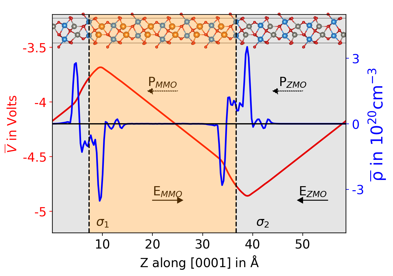
In Fig. 2 we show the calculated macroscopic averaged total charge density and electrostatic potential profile along the [] direction obtained directly from ZMO/MMO heterostructure calculation. The procedure of macroscopic averaging is to wash out unwanted periodic oscillations Colombo et al. (1991) coming from lattice periodicities of each constituent materials. The macroscopic averaged electrostatic potential shows the linear behaviour in the bulk of the material, indicating constant electric field. From the slope of in the linear region, we calculate the electric field inside the material (Table. S2). Moreover, the total charge density , shows charges only close to the interface but not in the bulk regions. The surface charge densities at heterostructure interface have been calculated by integrating (Table. S2).
We then proceed to validate our polarization discontinuity hypothesis, by calculating the electric field and surface charges from electrostatic model. The charges at the heterostructure interface and the field inside the material can be computed from polarization discontinuity hypothesis using the electrostatic boundary conditions Betancourt et al. (2013). Consider a heterostructure with two materials of length and having dielectric constants and and zero field polarization and , respectively. Using periodic boundary condition, which ensures the net potential difference across the supercell is zero, the bound charges at the interface, , and the field inside the bulk of the materials, and , are given as Betancourt et al. (2013),
| (1) |
where,
| (2) |
We calculate the electronic dielectric constant by applying a small static homogeneous electric field () along [] direction and studying the response of the system using modern theory of polarization Umari and Pasquarello (2002); Souza et al. (2002)(Table. S2). The polarization discontinuity () is sum of piezoelectric () contribution developed in the MMO layer due to lattice mismatch strain and the spontaneous polarization () difference between ZMO and MMO. As the in-plane lattice parameters of ZMO and MMO are very close and the e31 value of MMO is quite small (), the piezoelectric effect is negligible. Using Eq. 1, we find the surface charge density to be which agrees perfectly with the value we find from heterostructure calculation earlier. Moreover, we find the electric fields inside each slab (EZMO = , EMMO = ) are also in very good agreement. See supplementary material for these comparisons (Table. S2).
The agreement between results obtained from heterostructure calculation and from Eq. 1 which is derived assuming polarization discontinuity hypothesis proves that the surface charge density in this heterostructure is indeed due to polarization discontinuity at the interface. The electric field created by these bound surface charges bring any free carriers created inside the bulk of the material to the interface making a 2DEG (or 2DHG). It is important to note that in a real material the formation of 2DEG (or 2DHG) in some cases may be hindered by formation of defects such as Oxygen vacancies Zhong et al. (2010). In Fig. 3(a) we show the layer-resolved Mo(4d) DOS. We have also performed the same calculation with increasing the thickness of both ZMO as well MMO layers (Fig. S3). We choose Mo(4d) states because both the valence and conduction band edge of all A2Mo3O8 compounds are mostly of Mo(4d) character (Fig. 1(c)). The layer-resolved Mo (4d) DOS clearly shows the shift in the valence and conduction bands due to the in-built electrostatic field inside the heterostructure as we go along [] direction. From Fig. 3(a) (also from layer dependent band structure in Fig. S2) it is evident that conduction and valence band edge of the heterostructure is composed of states localized near one of the two interfaces in the heterostructure. It should be noted that the linear nature of the potential inside the bulk region is the consequence of the absence of free carriers in our calculation. In real materials free carriers will screen the bound surface charges at the interface. As a results one will not see a linear region inside the material as in Fig. 2. Instead the potential will saturate as one goes away from the interface Betancourt et al. (2013) such that the field far from the interface becomes zero. Nevertheless, free carriers will be localized at the interface by the electric field of polarization induced bound charges. In principle, free carriers in real materials can be generated both spontaneously or as a result of modulation doping. In GaAs/Al(Ga)As heterostructure, the free carriers are provided by the modulation doping. In case of GaN/Al(Ga)N heterostructure it has been observed that donor states at the surface can provide free carriers in the system Heikman et al. (2003). The origin of free carriers, while interesting, is outside the scope of the present study.
To study the localization of the 2DEG (or 2DHG) in the ZMO/MMO heterostructure, we simulate the addition of free carriers in the system by moving the Fermi level upwards into the conduction band (-doping) or downwards into the valence band (-doping). We move the Fermi level of the system such that we add (remove) 0.003 to (from) the heterostructure supercell. This corresponds to a surface charge density of . In Fig. 3(b) we plot where s are the occupied (emptied) states as a result of doping. Blue and red lines have been used to show the electron density in case of -doping and hole density is case of -doping respectively. As one can see from Fig. 3(b), both the 2DEG as well as 2DHG is well localized to within from the interface. The strong localization at the interface is a consequence of the fact that the excess carriers due to doping occupy interfacial Mo(4d) states which are localized in the [0001] direction.
| Interface | in | in |
|---|---|---|
| ZMO/MMO | 0.028 | 0.403 |
| ZMO/CMO | 0.053 | 0.647 |
| MMO/CMO | 0.082 | 1.088 |
In Table. 2 we list the surface charge densities for different possible A2Mo3O8/B2Mo3O8 interface. The values are calculated using Eq. 1, as we expect polarization discontinuity driven 2DEG (or 2DHG) to form in case of other heterostructure like ZMO/CMO and MMO/CMO as well. We can see the value of surface charge density is highest for MMO/CMO interface due to largest polarization discontinuity. These values are comparable to other well known heterostructure systems that has been found to host 2DEG such as GaN/Al(Ga)N or ZnO/Zn(Mg)O Heikman et al. (2003); Tampo et al. (2008), in which the surface charge densities were found to be of the order of . This suggests that the A2Mo3O8/B2Mo3O8 interface can be a strong candidate for hosting 2DEG/2DHG in an all oxide system.
In this work we explore the possibility of 2DEG formation in a novel heterostructure system. The materials forming these heterostructure has the chemical formula A2Mo3O8 where A can be Zn, Mg or Cd. All these materials have been synthesized before and found to be very stable. We calculate the piezoelectric properties of these materials by applying an external strain and studying the response of the system. We also compute the value of spontaneous polarization of these materials using Berry phase method. We then proceed with DFT calculation of slab based heterostructure system consists of ZMO and MMO. We show that there are localized surface charges at the interface and electrostatic field inside the material. We show that these bound charges are due to polarization discontinuity at the interface. We show excellent agreement of surface charge density and electric field values between heterostructure calculation and polarization discontinuity model. We then simulate doping of the system by moving the fermi level of the system and show that the additional charges are localized within from the interface. We also report the values of surface charge densities for other possible heterostructure system of these materials such as ZMO/CMO or MMO/CMO. We show that the surface charge densities in these systems are comparable to other well known heterostructure system that forms 2DEG, such as AlN/Al(Ga)N or ZnO/Zn(Mg)O.
I Acknowledgment
The authors thank Prof. Rajeev Ranjan, Prof. Srimanta Middey, Prof. Sumilan Banarjee, Prof. S. Raghavan and Prof. S. Avasthi for useful discussions. This work is supported under the US-India Partnership to Advance Clean Energy-Research (PACE-R) for the Solar Energy Research Institute for India and the United States (SERIIUS), funded jointly by the U.S. Department of Energy (Office of Science, Office of Basic Energy Sciences, and Energy Efficiency and Renewable Energy, Solar Energy Technology Program, under Subcontract DE-AC36-08GO28308 to the National Renewable Energy Laboratory, Golden, Colorado) and the Government of India, through the Department of Science and Technology under Subcontract IUSSTF/JCERDC-SERIIUS/2012 dated 22nd Nov. 2012. We thank Super Computer Research and Education Centre (SERC) at IISc for the computational facilities.
References
- Imada et al. (1998) M. Imada, A. Fujimori, and Y. Tokura, Reviews of Modern Physics 70, 1039 (1998).
- Rao (1989) C. Rao, Annual Review of Physical Chemistry 40, 291 (1989).
- Chakhalian et al. (2012) J. Chakhalian, A. Millis, and J. Rondinelli, Nature Materials 11, 92 (2012).
- Chakhalian et al. (2014) J. Chakhalian, J. W. Freeland, A. J. Millis, C. Panagopoulos, and J. M. Rondinelli, Reviews of Modern Physics 86, 1189 (2014).
- Hwang et al. (2012) H. Y. Hwang, Y. Iwasa, M. Kawasaki, B. Keimer, N. Nagaosa, and Y. Tokura, Nature Materials 11, 103 (2012).
- Schlom et al. (2008) D. G. Schlom, L.-Q. Chen, X. Pan, A. Schmehl, and M. A. Zurbuchen, Journal of the American Ceramic Society 91, 2429 (2008).
- Abrahams et al. (2001) E. Abrahams, S. V. Kravchenko, and M. P. Sarachik, Reviews of Modern Physics 73, 251 (2001).
- Anderson (1960) R. Anderson, IBM Journal of Research and Development 4, 283 (1960).
- Delagebeaudeuf and Linh (1982) D. Delagebeaudeuf and N. T. Linh, IEEE Transactions on Electron Devices 29, 955 (1982).
- Bristowe et al. (2014) N. Bristowe, P. Ghosez, P. B. Littlewood, and E. Artacho, Journal of Physics: Condensed Matter 26, 143201 (2014).
- Ohtomo and Hwang (2004) A. Ohtomo and H. Hwang, Nature 427, 423 (2004).
- Nakagawa et al. (2006) N. Nakagawa, H. Y. Hwang, and D. A. Muller, Nature Materials 5, 204 (2006).
- Thiel et al. (2006) S. Thiel, G. Hammerl, A. Schmehl, C. Schneider, and J. Mannhart, Science 313, 1942 (2006).
- Park et al. (2010) J. Park, D. Bogorin, C. Cen, D. Felker, Y. Zhang, C. Nelson, C. Bark, C. Folkman, X. Pan, M. Rzchowski, et al., Nature Communications 1, 94 (2010).
- Heikman et al. (2003) S. Heikman, S. Keller, Y. Wu, J. S. Speck, S. P. DenBaars, and U. K. Mishra, Journal of Applied Physics 93, 10114 (2003).
- Tampo et al. (2008) H. Tampo, H. Shibata, K. Maejima, A. Yamada, K. Matsubara, P. Fons, S. Kashiwaya, S. Niki, Y. Chiba, T. Wakamatsu, et al., Applied Physics Letters 93, 202104 (2008).
- Betancourt et al. (2013) J. Betancourt, J. Saavedra-Arias, J. D. Burton, Y. Ishikawa, E. Y. Tsymbal, and J. P. Velev, Physical Review B 88, 085418 (2013).
- McCarroll et al. (1957) W. H. McCarroll, L. Katz, and R. Ward, Journal of American Chemical Society 79, 5410 (1957).
- Paranthaman et al. (1988) M. Paranthaman, G. Aravamudan, and G. S. Rao, Bulletin of Materials Science 10, 313 (1988).
- Biswas et al. (2017) T. Biswas, P. Ravindra, E. Athresh, R. Ranjan, S. Avasthi, and M. Jain, The Journal of Physical Chemistry C 121, 24766 (2017).
- Wang (2012) Z. L. Wang, Advanced Materials 24, 4632 (2012).
- Giannozzi et al. (2009) P. Giannozzi, S. Baroni, N. Bonini, M. Calandra, R. Car, C. Cavazzoni, D. Ceresoli, G. L. Chiarotti, M. Cococcioni, I. Dabo, et al., Journal of Physics: Condensed Matter 21, 395502 (2009).
- Schlipf and Gygi (2015) M. Schlipf and F. Gygi, Computer Physics Communications 196, 36 (2015).
- Perdew and Zunger (1981) J. P. Perdew and A. Zunger, Physical Review B 23, 5048 (1981).
- King-Smith and Vanderbilt (1993) R. King-Smith and D. Vanderbilt, Physical Review B 47, 1651 (1993).
- Bernardini et al. (1997) F. Bernardini, V. Fiorentini, and D. Vanderbilt, Physical Review B 56, R10024 (1997).
- Ederer and Spaldin (2005) C. Ederer and N. A. Spaldin, Physical Review Letters 95, 257601 (2005).
- Dal Corso et al. (1994) A. Dal Corso, M. Posternak, R. Resta, and A. Baldereschi, Physical Review B 50, 10715 (1994).
- Shieh et al. (2009) J. Shieh, J. Yeh, Y. Shu, and J. Yen, Materials Science and Engineering: B 161, 50 (2009).
- Günter (1977) P. Günter, Journal of Applied Physics 48, 3475 (1977).
- Colombo et al. (1991) L. Colombo, R. Resta, and S. Baroni, Physical Review B 44, 5572 (1991).
- Umari and Pasquarello (2002) P. Umari and A. Pasquarello, Physical Review Letters 89, 157602 (2002).
- Souza et al. (2002) I. Souza, J. Íniguez, and D. Vanderbilt, Physical Review Letters 89, 117602 (2002).
- Zhong et al. (2010) Z. Zhong, P. Xu, and P. J. Kelly, Physical Review B 82, 165127 (2010).