Type-II Dirac line node in strained Na3N
Abstract
Dirac line node (DLN) semimetals are a class of topological semimetals that feature band-crossing lines in momentum space. We study the type-I and type-II classification of DLN semimetals by developing a criterion that determines the type using band velocities. Using first-principles calculations, we also predict that Na3N under an epitaxial tensile strain realizes a type-II DLN semimetal with vanishing spin-orbit coupling (SOC), characterized by the Berry phase that is -quantized in the presence of inversion and time-reversal symmetries. The surface energy spectrum is calculated to demonstrate the topological phase, and the type-II nature is demonstrated by calculating the band velocities. We also develop a tight-binding model and a low-energy effective Hamiltonian that describe the low-energy electronic structure of strained Na3N. The occurrence of a DLN in Na3N under strain is captured in the optical conductivity, which we propose as a means to experimentally confirm the type-II class of the DLN semimetal.
I Introduction
During the past decade, topological semimetals have been an active subject of condensed matter physics and quantum materials, providing a unique venue for exotic phenomena originated from band topology Arnold et al. (2016); Zhang et al. (2016); Li et al. (2016a); He et al. (2014). Since the discovery of Weyl semimetals Burkov et al. (2011); Wan et al. (2011); Yang et al. (2011); Xu et al. (2011a); Singh et al. (2012); Huang et al. (2015); Xu et al. (2015a, b); Weng et al. (2015a); Lv et al. (2015); Xu et al. (2016, 2015c); Jia et al. (2016), various classes of topological semimetals have been found theoretically and experimentally, including Dirac semimetals Xu et al. (2011b); Liu et al. (2014a); Wang et al. (2012); Young et al. (2012); Borisenko et al. (2014); Wang et al. (2013); Liu et al. (2014b); Kim et al. (2015); Yu et al. (2015), nodal line semimetals Burkov et al. (2011); Yu et al. (2016a); Fang et al. (2016); Weng et al. (2016a); Chiu et al. (2016); Fang et al. (2015); Kim et al. (2015); Yu et al. (2015); Xu et al. (2017); Huang et al. (2016a); Young et al. (2017); Zhao et al. (2016); Du et al. (2017); Weng et al. (2015b); Chen et al. (2015); Wang et al. (2016a); Cheng et al. (2016); Ezawa (2016); Hirayama et al. (2017); Li et al. (2016b); Gan et al. ; Weng et al. (2016b); Zhu et al. (2016); Lu et al. ; Xie et al. (2015), and their diverse variations such as multi-Weyl semimetals and double Dirac semimetals Fang et al. (2012); Wieder et al. (2016); Huang et al. (2016b); Bradlyn et al. (2016); Chang et al. (2017).
More recently, the classification of topological semimetals is further specified into the type-I and type-II classes based on the geometric structure of the Fermi surface Soluyanov et al. (2015); Wang et al. (2016b); Deng et al. (2016); Autès et al. (2016); Kim et al. (2017); Yan et al. (2017); Huang et al. (2016c); Chang et al. (2017). The type-I material features a closed Fermi surface enclosing the nodes; in contrast, type-II material features open Fermi surface composed of electron and hole pockets that linearly touch at the nodes. First proposed in Weyl semimetals, the type-I/II classification has been extended to Dirac semimetals Zhang et al. (2017); Noh et al. (2017); Fei et al. (2017); Kim et al. (2017); Guo et al. (2017); Chang et al. (2017) and nodal line semimetals Li et al. (2017); Chang et al. ; He et al. . In the case of Weyl semimetals, such classification provides an important insight for understanding unique phenomena present only in the type-II materials, such as the squeezing or collapse of the Landau levels, the Klein tunneling, and magnetic breakdown in momentum space when magnetic fields are applied to over-tilted Weyl nodes O’Brien et al. (2016); Yu et al. (2016b); Tchoumakov et al. (2016); Alexandradinata and Glazman (2017). Some papers have already proposed type-II DLNs and reported relevant materials hosting such kinds of DLNs Li et al. (2017); Chang et al. ; He et al. . Contrasting features of type-I and type-II DLNs have been identified in terms of their dispersion and Fermi surface geometry Li et al. (2017).
In this paper we go beyond the well-known characterization of type-II DLNs and identify a more fundamental way to understand and identify the type-II class of DLN semimetals. Based on geometric argument, a concrete connection is established between the sign inversion of band velocities around a type-II DLN and the occurrence of open Fermi surface in type-II DLN semimetals, which leads to a rigorous criterion to determine the types of DLNs. We use this criterion and first-principles calculations to predict that epitaxially strained Na3N realizes a type-II DLN semimetal phase. The nontrivial band topology and type-II nature of the DLN semimetal are explored. We also construct a tight-binding model and a low-energy effective theory, and use them to rationalize the low-energy electronic structure and to calculate the optical conductivity of Na3N. The optical response significantly changes upon straining due to the occurrence of a type-II DLN semimetal, which can be experimental evidence of the type-II DLN semimetal phase hosted in strained Na3N.
This paper is structured as follows. First, we begin with the background in Sec. II, which provides simple and intuitive ways to understand the type-I versus type-II nature of DLNs. Following that, we contrast in Sec. III the electronic band structures of pristine and strained Na3N. This clarifies the electronic structure of Na3N that is responsible for the occurrence of a DLN under strain. Next, in Sec. IV, topological characterization of strained Na3N is discussed in terms of topological indices and surface energy spectrum. Also, the type-II nature is demonstrated via the band velocities evaluated in the vicinity of the DLN. Then, in Sec. V, we construct a tight-binding model for Na3N, reproducing main features of the DFT calculations. Physical manifestations of the type-II DLN nature are predicted to occur as unique features in the surface spectrum and the optical conductivity, as demonstrated in Sec. VI. Finally, we conclude the paper with a summary and perspective in Sec. VII.
II Backgrounds
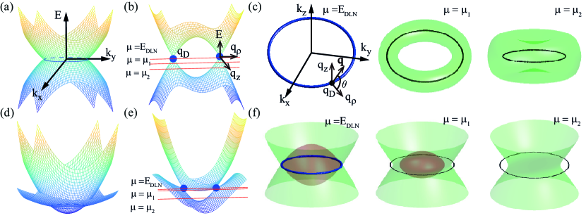
We start with a brief review of the mathematical foundation for the type-II DLN semimetals. Similar to the Weyl semimetal case Soluyanov et al. (2015), distinguishing aspects of type-II DLNs lie in their dispersion and the Fermi surface geometry: the existence of over-tilted Dirac cone and the open (or extended) Fermi surface Li et al. (2017). Figure 1(a) and (d) illustrate the contrasting shape of energy bands of type-I and type-II DLNs on the plane where the line node lies. Also, Fig. 1(b) and (e) show contrasting energy bands of type-I and type-II DLNs featured on the plane for a fixed value of in-plane angle , where is the radial momentum. The plane intersects with the DLN at two points of the DLN. The intersecting points of the DLN and the plane are indicated by blue dots in Figs. 1(b) and (e). These intersecting points appear as Dirac points with linear dispersions away from the points on this normal plane. Hereafter, we refer to them as Dirac points.
While the energy dispersions are linear in both type-I and type-II DLNs in the vicinity of the nodal line, the difference between them is clear in the band velocities at the DLN. Recall that two independent directions exist in moving away from a given point on the DLN, which define a plane locally normal to the tangent direction of the DLN. If the band velocities are opposite for the conduction and the valence bands regardless of the direction away from the Dirac point in this normal plane, we refer to this as a conventional type-I DLN. In contrast, if the band velocities of the conduction and valence band have the same sign for some direction away from the DLN in the normal plane, we refer to it as an unconventional type-II DLN. These different types give rise to the second distinguishing characteristic, manifested in the Fermi surface geometry. As illustrated in Fig. 1(c) and (f), as one varies the chemical potential [red lines in Fig. 1(b) and (e)], hole (electron) pocket appears as a green (red) surface. Irrespective of the chemical potential , the Fermi surface (equally, constant energy surface at ) of a type-I (type-II) DLN exists in a closed (open) surface, in line with the previous study in Li et al. (2017).
Instead of inspecting the band velocities, the classification is also possible by the Fermi surface geometry, similar to the case of Weyl points Soluyanov et al. (2015). To specify this, we first introduce two coordinate systems used in the discussion throughout the paper. The first one is the coordinates in the Brillouin zone (BZ) describing the global structure of a DLN. The second set of coordinates is a relative coordinate system with the origin at a Dirac point of the DLN [Fig. 1(c)], which describes the local behavior of the energy bands. The two coordinate systems are related by , where refers to a point on the DLN.
In general, the nodal structure of two bands can be described by Hamiltonian
| (1) |
with the Pauli matrices ’s. When the Hamiltonian is linear in , one can find a linear map from to , where , , and
| (2) |
Band gap clossing points generically occur at the -points that satisfy for all ’s. Depending on the dimensions of the null space (or kernel space) of the linear map , which can be either 0, 1, or 2, the gap closing points constitute points, lines, or planes, respectively. The kernel dimensions determine the dimensions of the quotient space and also the dimensions of the image space of the linear mapping imA as . We can rewrite the low-energy Hamiltonian using the new linear mapping from to imA with reduced dimensions (, and ). Now this new linear mapping describes only the linear dispersion in the two directions that are locally orthogonal to the nodal line direction. As a result, in the case of nodal line [Dim kerA=1], the local behavior of electrons is described by the low-energy Hamiltonian with the reduced dimensions. [Dim =2]
| (3) |
Here “local” means that the wave vector is expanded from a particular point on the nodal line [See Fig. 1(c)]. Representing the position of a point constituting the DLN as , wave vectors in the BZ are expanded up to the linear order of , leading to the low-energy Hamiltonian Eq. (3) that describes a Dirac cone in two dimensions. The second term in the Hamiltonian is introduced to describe the tilting of the Dirac cones, which plays a crucial role enabling the type-II DLNs. As in the case of the Weyl point (WP) Soluyanov et al. (2015), the Fermi surface equation, which is a conic section equation in the DLN case, gives either an open or a closed solution, which defines the type-I/type-II classifications.
In detail, two energy eigenvalues are obtained from Eq. (3) as
| (4) |
The Fermi surface equation that satisfy is obtained as
| (5) |
When det() 0 , Eq. (5) describes a conic section equation that gives an elliptic (a hyperbolic) curve. Thus, DLNs are classified into two types: type-I for the elliptic (closed) curve and type-II for parabolic (open) curve. It should be worthwhile to mention that, in general, the tilting coefficient can be a function of , although it is treated as a constant for simplicity in the above derivation. When the tilting coefficient varies, such that det() changes the sign along the DLN, which can happen in highly anisotropic systems that reside near the transition between this type-I and type-II, the sign change of the determinant identifies a novel-type hybrid DLN Chen et al. (2018). While this case shares the characteristic features of type-II DLNs hosting the electron and hole pockets that coexist with the DLN, it also allows for diverse possibilities in the Fermi surface geometry, which could be of a particular interest with respect to quantum oscillations and transport phenomena.
Another way of sorting out the types of DLNs is by looking at the sign inversion of band velocities. Since the matrix is Hermitian with non-negative eigenvalues (we assume the generic situation of non-zero eigenvalues), the energy dispersion after the rotation to the principal axis becomes
| (6) |
After the rescaling of variables , and introducing the polar coordinates one can further simplify the energy equation [Eq. (6) ] to
| (7) |
Here, measures the angle from one of the principal axes. The conventional type-I Dirac cone shown in Fig. 1(b) is realized if the radial velocity satisfies for all orientations , or equivalently, when
| (8) |
Otherwise, the unconventional type-II Dirac cone shown in Fig. 1(e) is realized with over some range of . After some unraveling of the algebra, one can prove that Eq. (8) is equivalent to the condition . This proves that the classification scheme in terms of the conic section is equivalent to the one in terms of the sign inversion of the band velocity.
The difference in the type-I and type-II band structures can be understood in the language of differential geometry as well. The band velocities along the principal axes are the well-known principal curvatures in differential geometry, and their product is the Gaussian curvature that indicates the shape of the surface. For either the conduction band or the valence band [ in Eq. (7)], coordinates along the principal axes are and the corresponding velocities (or principal curvatures) are given by , respectively. The Gaussian curvatures for each band follows from . In type-I (type-II) DLNs, the product of Gaussian curvatures
| (9) |
are positive (negative). The final expression on the right follows from Eq. (8). As a result, all three methods, i.e. conic section classification, sign inversion of band velocity, and band curvature analysis, yield the same conclusion in regard to the type-I/II classification of DLNs. In the type-II DLN, either the conduction band or the valence band has the saddle-shaped band structure in the space.
III Methods and
Electronic band structure
III.1 Calculation methods
Having identified the physical and mathematical conditions to distinguish the type-I and type-II DLNs, we now show that Na3N under strain realizes a type-II DLN. Before showing the first-principles results, we list the details of computational methods. Our first-principles calculations are based on density functional theory (DFT) in the Perdew–Zunger–type local density approximation (LDA) Perdew and Zunger (1981). The norm–conserving, optimized, designed nonlocal pseudopotentials are generated using opium Rappe et al. (1990). The wave functions are expanded in plane–wave basis as implemented in quantum espresso package Giannozzi et al. (2009). The energy cutoff for the basis is set to 680 eV. The atomic structure is fully relaxed within the force threshold of 0.005 eV/Å and the 888 Monkhorst-Pack grid Monkhorst and Pack (1976) is used for -points sampling. The surface spectra are obtained by calculating the surface Green’s function for a semi-infinite geometry Sancho et al. (1984, 1985), using the Wannier Hamiltonian, generated using Wannier90 Marzari et al. (2012); Marzari and Vanderbilt (1997); Mostofi et al. (2008); Souza et al. (2001). For the Wannierization, the conduction and valence states are initially projected to the orbitals of K and Na, and the orbitals of N, for the wannierization. The lattice constant of Na3N is calculated as = 4.67 Å. The lattice constants of strained Na3N is calculated by fixing and relaxing the other lattice parameter. In the case of 5 % of tensile strain, we fixed to 4.91 Å, and relaxed , resulting in 4.63 Å. The Poisson ratio for the epitaxial strain is calculated as 0.2. In order to show the robustness of our LDA results, the hybrid functional calculation for the electronic band structure is performed using vasp Kresse and Furthmüller (1996), employing the Heyd-Scuseria-Ernzerhof (HSE06) scheme for exchange-correlation potential Heyd et al. (2003). Although SOC is negligibly weak in Na3N, the effect of SOC is considered in the Appendix B for the sake of completeness of the study by using full-relativistic pseudopotentials based on non-collinear spin calculations.
III.2 Crystal structure and symmetries
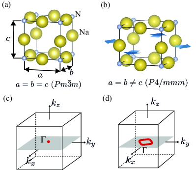
Figure 2(a) illustrates the primitive unit cell of Na3N in anti-ReO3 structure, which comprises one N atom at the corner and three Na atoms at the center of each edges. The crystalline symmetries belong to the cubic space group Pmm (#221), generated by inversion and three rotations. Under an epitaxial strain shown in Fig. 2(b), the cubic crystalline symmetry is broken into the P4/mmm (#123) tetragonal space group symmetry. The P4/mmm space group is generated by inversion , reflection , and the four-fold rotation . Together with these crystalline symmetries, time-reversal symmetry plays an important role to provide topological protection of the DLN. Here is the complex conjugation operator. Figure 2(c) and (d) show the BZ of pristine Na3N and strained Na3N, respectively. We find that the point in pristine Na3N host a triply-degenerate state (not counting the spin degeneracy), which evolves into a DLN encircling lying on the plane under the strain. The evolution of the triply degenerate point to a DLN is detailed in subsection IV.1.
III.3 Electronic band structure
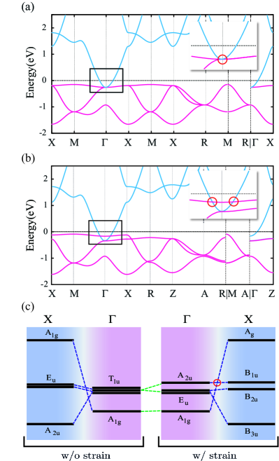
Figure 3(a) and (b) show the electronic band structures of pristine and 5 % epitaxially tensile strained Na3N obtained from our first-principles calculations without spin-orbit coupling. It is clear that the band structures of both cases are semimetallic, with the electron and hole pockets forming near the and points, respectively. As it is well known that LDA tends to underestimate the band gap (equally, overestimate the band inversion), we also calculated the HSE06 band structure and find that the semimetallic feature is reproduced 111See Appendix A for the HSE06 results.. Nonetheless, it is worth mentioning that, depending on the exchange-correlation functionals, the band structure of Na3N could be semiconducting. Indeed, some literature Vajenine (2008); Sommer et al. (2012) claims that Na3N is a semiconductor when a different exchange-correlation energy functional is used. We discuss this further in Sec. VII. We point out that the remainder of the discussion is based on our LDA and HSE06 results.
IV Type-II DLN in strained Na3N
As illustrated in Fig. 2(d), an epitaxial tensile strain applied to Na3N engenders a DLN of the type-II class. In this section, we first show that strained Na3N hosts a DLN in momentum space. The crossing points that we found off the high symmetry point in the band structure indicate the presence of a DLN. From this indication, we identify the states forming the DLN and clarify the geometry of the DLN in the BZ. Next, we discuss the topological protection by calculating topological invariants that dictate the presence of DLNs Kim et al. (2015). Finally, we show the type-II nature of the DLN. For this purpose, we construct a Hamiltonian and an explicit tight-binding model that reproduce the DFT band structure, and apply the type-I/type-II criterion derived in II, which confirms the type-II class. For further demonstration of the type-II nature, we present the unconventional linear dispersion occurring along principal axes from our DFT calculations. We also calculate the numerical value of the principal curvatures, resulting in the Gaussian curvatures with opposite sign, which reaffirms the type-II nature.
IV.1 DLN
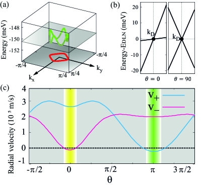
The low-energy electronic structure near the Fermi energy governs the topological property of Na3N. At , we find that the valence band top and the conduction band bottom are fused to form a triply-degenerate state right below the Fermi level, indicated by a red circle in the inset of Fig. 3(a). In addition, a single state resides 0.67 eV below the state at . An epitaxial strain gives rise to a tetragonal crystal field, which splits the triply-degenerate state into a doubly-degenerate state and a single state. Tensile (compressive) strain raises (lowers) the energy of the state with respect to the doubly-degenerate state at . The energy-lowering of under a tensile strain enables the crossing between and bands. Notably, the crossing does not happen when applying the compressive strain that raises the energy of state. The inversion of the and states is responsible for the occurrence of a DLN in strained Na3N, which occurs along the high-symmetry lines or . This results in band-crossing points indicated by red circles in Fig. 3(b) and (c). Careful inspection of the band structure in the entire BZ allows us to find a single DLN encircling that lies on the plane as shown in Fig. 4(a). The DLN is located at eV below the Fermi energy, with dispersion in the energy range of eV.
IV.2 Topological protection
The protection of the DLN is two-fold. First, lying on the mirror-invariant plane, the DLN is protected by with the conduction and valence bands having different mirror eigenvalues . In addition, the DLN is also topologically protected by inversion and time-reversal symmetries Kim et al. (2015); Yu et al. (2015). Judging from the group representation of the Bloch states forming the DLN, we find the band inversion at between and states, which are odd and even parity eigenstates of inversion , respectively. These two states are also mirror eigenstates having opposite parities, leading to the mirror-protected band crossing on the mirror-invariant plane . The presence and geometric shape of a DLN in momentum space is dictated from the topological indices as discussed in Ref. Kim et al. (2015). We find for strained Na3N from parity analysis at the time-reversal invariant momenta (TRIMs) , which agree with the existence and shape of the DLN. In detail, enforces an odd number of DLNs to thread the half -invariant plane containing . This is fulfilled by the DLN encircling the lying on the plane.
IV.3 analysis and type-II nature
In this section, we construct the Hamiltonian that describes the DLN, and confirm its type-II nature. The Hamiltonian near can be constructed such that it respects the little group symmetries of on the basis and
| (10) | |||||
Here , and ’s are the Pauli matrices in (A2u, A1g) basis, and , , , and are constants. The DLN forms along a circle on the plane. The first term of Eq. (10) induces tilting that enables the type-II nature of the DLN. The best match to the DFT band structure in the vicinity of the point for pristine and 5 %-strained Na3N is found when using the parameters listed in Table 1 222See Appendix C more parameter sets for 1%, 2%, 3%, and 4%-strained cases.. In the pristine case, where , , , and , the energy state are degenerate at [], exhibiting isotropic band structure originated from the cubic symmetry. The tensile strain reduces the cubic symmetry to tetragonal symmetry, described by non-zero values for the velocity and the radius of the DLN , as well as the difference between the values of and .
| Parameters | Pristine | 5 %-strained |
|---|---|---|
| 5.00 | 5.00 | |
| 4.60 | 4.60 | |
| 5.00 | 4.00 | |
| 4.60 | 3.80 | |
| 0.00 | 1.05 | |
| 0.00 | 0.14 |
As previously pointed out in Sec. II, the Hamiltonian can be expanded in in the vicinity of a point on the DLN
| (11) |
which is of the same form as Eq. (3) with the principal axes and . The type-II criterion previously worked out in Sec. II is simplified as
| (12) |
which is consistent with the previously proposed type-I/type-II classification of DLNs Li et al. (2017). As shown in Table 1, 5 %-strained Na3N indeed satisfies Eq. (12), thus confirming the type-II DLN semimetal phase.
The type-II nature is further illustrated from the shape of Dirac cones. Figure 4(b) illustrates the band structures drawn along the () and () directions, which are the principal axes of the Hamiltonian. We find that the unconventional (left panel) and conventional (right panel) linear dispersions coexist in the vicinity of the Dirac point, which is a characteristic of the unconventional type-II DLN. Figure 4(c) shows the radial band velocities around the DLN as a function of calculated from the DFT band structures. Conventional (unconventional) linear dispersion resides in grey (yellow and green) region, resulting in (), which proves the sign change in the band velocities. Additionally, it is manifested that either the conduction or the valence band is a saddle-shaped band undergoing the sign flip of the radial band velocity, resulting in . This is a characteristic of the radial band velocities only present in a type-II DLN semimetal. In a type-I DLN semimetal, should be positive for the entire range of , resulting in .
V Tight-binding model analysis
The tight-binding model is a useful way to develop the low-energy effective theory for the DLN. We construct it using the basis of -orbitals of the N atom and the -orbital of Na. The basis orbitals are thus (N , N , N , Na- , Na- , Na- ), where Na- is the Na atom at , Na- at , and Na- at , respectively. We arrive at the tight-binding Hamiltonian written as a block form
| (13) |
The submatrices , concern the three -orbitals of N and the three inequivalent -orbitals of Na, respectively. is their hybridization. In detail,
| (14) |
Here, the abbreviations are used for , , , , , . The on-site energies of N and Na orbitals are denoted as and , respectively, which are set to the same values both in pristine and strained cases.
We consider the hopping between the basis orbitals up to third nearest neighbors in the pristine and strained crystal structure. For the nearest neighbor hopping, the hopping integral between the orbital at the origin and the -orbital of the Na- atom is denoted as . In the pristine case, the cubic symmetry enforces . In the strained case, the lowered symmetry differentiate from . We denote the as and as , respectively. The second-nearest neighbor hopping takes place between Na- and Na-, or between equivalent Na atoms. The corresponding hopping integrals are denoted as for Na- to Na- , and for Na- to Na- , or Na- to Na- . One can expect only for the pristine cubic crystal of Na3N. The third-nearest neighbor hopping takes place between the orbitals of N atoms in the adjacent unit cells [distanced by ], parameterized by the hopping integrals . Considering and symmetry between orbitals, we obtain the constraints for the pristine and strained cases. In the pristine case, there is no difference among , , and -directions. Therefore, there are only two types of distinct hopping integral and . In contrast, there are four different third neighbor hopping integral , , , and in the strained case. In the tetragonal-symmetric case, represents and . On the other hand, represents The on-site energies and hopping integrals for pristine (strained) cases are listed in Table 2 (3). A negative value of the hopping parameter is responsible for the DLN belonging to the type-II class. A type-I DLN occurs for positive .
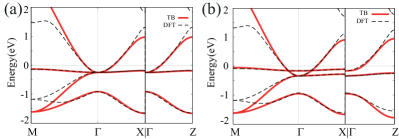
Close fits to both pristine and strained DFT bands are achieved in Fig. 5 using the tight-binding parameters in Table 2. Near the point, the DLN occurs. The tight-binding model corroborates the following DFT results. The line node is formed via the band inversion between the odd-parity eigenstate composed of N orbital, and the even-parity eigenstate composed of three -orbitals from Na-, Na-, and Na-. In both cases, the even parity state is below the odd parity eigenstate at , while the even parity state is above the odd parity eigenstates in other seven TRIM points. The strain opens the band gap between and states at the eight TRIM points, resulting in non-trivial topological invariant. Based on the tight-binding parameters of Table 3 we also reproduced the same topological invariants as the DFT results.
| On-site energy | Value (eV) |
|---|---|
| -2.45 | |
| +0.85 | |
| Hopping integral | |
| -1.00 | |
| -0.47 | |
| -0.13 | |
| -0.015 |
| On-site energy | Value (eV) |
|---|---|
| -2.45 | |
| +0.85 | |
| Hopping integral | |
| -0.95 | |
| -0.95 | |
| -0.46 | |
| -0.47 | |
| -0.13 | |
| -0.205 | |
| -0.014 | |
| -0.025 |
VI Physical manifestations
In this section, we discuss feasible ways to detect the type-II DNL character of strained Na3N. Two physical manifestations are suggested: topological surface states and optical conductivity that we discuss in the following subsections. We suggest that the two can help clarify the topological and type-II nature of the DLN hosted in strained Na3N, respectively.
VI.1 Topological surface states
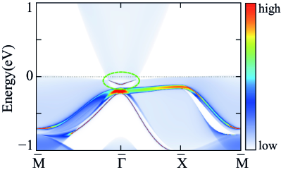
A topologically protected DLN features drumhead-like surface states Burkov et al. (2011); Kim et al. (2015); Yu et al. (2015); Weng et al. (2015b). We confirm this topological characteristic of the surface energy spectra using the surface Green’s function. Figure 6 shows the resultant surface band structure of the (001) surface for the semi-infinite slab of Na3N, drawn along projected high-symmetry lines following path of the square lattice. As the bulk DLN is parallel to the (001) surface, the interior region of the DLN is projected to a finite area of the surface BZ near . The region shaded by a bluish color in Fig. 6 shows the projected bulk states. The type-II nature is revealed in the unconventional (tilted) linear dispersion appearing on and , as shown in Fig. 6.
The high-intensity branch connecting the two crossing points is the topological surface states. They appear in the interior region of the projected DLN enclosing , indicated by the green circle. This explicitly proves the topological nature of strained Na3N. As discussed in the Ref. Kim et al. (2015), the curvature of the surface states is in part determined by the harmonic average of the curvatures of the conduction and valence bands. Our DFT calculations also feature this, yet due to the same sign of the curvature for the conduction and valence bands, the topological surface states appear more dispersive than nearly flat surface bands of a type-I DLN. This is another characteristic feature of a type-II DLN semimetal captured in the surface energy spectrum. We also note that there is high intensity contribution from the bulk states to the surface energy spectrum, originated from non-dispersive bulk bands along the direction, comprising mainly the N orbitals. We suggest that these non-topological states should be well-separated from the topological drumhead-like states when the strain is applied beyond the 4 % of tensile strain, making clear distinction between the topological surface states from the bulk trivial states.
VI.2 Optical conductivity
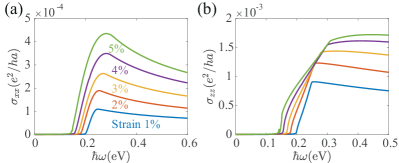
The optical conductivity of DLN semimetals has been studied in the previous literature and is known to exhibit a flat behavior at low frequencies below the nodal ring energy scale Ahn et al. (2017); Carbotte (2017). In this subsection, we investigate the optical responses of Na3N for both the pristine and strained cases. We demonstrate that the strain results in a qualitative change in the optical conductivity, suggesting that the optical signal of Na3N could serve as an experimental footprint for the ocurrence of the DLN under strain.
To obtain the optical conductivity, we evaluate the Kubo formula using the two-band effective model in Eq. (10). In the linear response and clean limit, the Kubo formula for the optical conductivity Mahan (2013) is written as
| (15) |
where , and are the eigenenergy and the Fermi distribution function for the band index and wave vector , respectively, is the chemical potential and with the velocity operator .
We first consider the pristine case. By applying the pristine parameters in Table 1 to Eq.(10), we obtain the effective Hamiltonian . The energy eigenstates and the velocity operator can be represented as the eigenstates of and , respectively. Using these, it is readily shown that the matrix element , and thus the interband transitions are forbidden in the pristine case. In contrast, in the strained case, the interband transitions are allowed, thus resulting in the non-zero optical response. The non-zero velocity term [ in Eq.(10)] makes the wavefunctions -dependent, leading to the non-vanishing matrix element for the interband transitions. We have calculated the interband optical conductivity as a function of strain; results for 1 % to 5 % are summarized in Fig 7 333See Appendix S1 for the parameters that we used to calculate the optical conductivities. Notably, both and exhibit a sudden increase at around for a given strain, which corresponds to the size of the optical gap arising from the Pauli blocking. Such a qualitative change upon straining the material, i.e., a sudden rise of the optical conductivity, is a key signature of the emergence of the Dirac line node induced by strain.
VII Discussion and Summary
In summary, we characterized a type-II topological DLN semimetal and proposed strained Na3N as its material realization. We showed that type-I/type-II DLNs can be classified in equivalent manner by the mathematical formalism governing any one of the three features: Fermi surface geometry, sign inversion of the band velocity, or the band curvature. We believe that these connections provide a fundamental and clear picture for the type-I/type-II classification of DLNs. In addition, the Type-II condition represented in terms of the band velocity should provide a computationally convenient way to determine the types of DLNs. Furthermore, our extensive DFT calculations predict that a type-II DLN semimetal should be realized in Na3N under epitaxial strain. We propose the drumhead surface states spectrum and optical conductivity as two key physical manifestations indicating the existence of a type-II DLN in strained Na3N. In particular, the optical response is expected to undergo a sudden jump under the strain due to a creation of a DLN, while the interband transition in pristine Na3N is suppressed by the selection rule. This feature should serve as an experimental evidence of the type-II DLN semimetal phase hosted in strained Na3N.
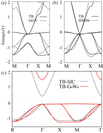
Encouragingly, the synthesis of pristine Na3N has been reported in the literature Dieter and Martin (2002); Niewa (2002); Vajenine (2007). However to the best of our knowledge, the literature disagrees with our DFT calculation. For example, an optical response of Na3N reported in Ref. Vajenine (2008) for visible light and near IR spectra results in a sizable optical band gap of 1.6 - 2.0 eV. Also, first-principles calculations based on self-interaction correction (SIC) and G0W0 methods support the experiment Sommer et al. (2012). Clearly, they stand in contrast with our calculation based on LDA and HSE. On the other hand, the band gap calculation based on the HSE06 hybrid functional, which reproduce experimental band gaps with a high degree of accuracy in some systems Lucero et al. (2011); Paier et al. (2009); Kim et al. (2010); Gillen et al. (2013); Moses et al. (2011), also shows the metallic behavior in line with the LDA and GGA calculations (see Appendix A).
As described in Sec. IV, the inversion of and bands at the point is a key ingredient for the formation of a DLN as well as the band gap. The band inversion is captured by the LDA or HSE06 calculation, but apparently not by the previous SIC or G0W0 calculations. To better understand the origin of this discrepancy, we made tight-binding fits to band structures of HSE06, SIC, and G0W0 as shown in the Appendix A. Compared to the estimation by the LDA results, other calculations gave an increase in the on-site energy of Na -orbitals given by +0.65, +1.10, and 2.25 eV, respectively. The dramatic increase in in the case of SIC and G0W0 is presumably responsible for the lack of band inversion at the point, as well as the consequent absence of a DLN. Tight-binding models deduced from fits of SIC and G0W0 bands gave the trivial topological number, as expected.
We believe that the metallicity of Na3N yet requires further confirmation via accurate band gap measurements, such as absorption spectra with low-energy photon energies or transport experiments. The previous experiment was performed using Na3N powders that could potentially contain excessive Na, as mentioned in the study Vajenine (2008). Therefore, existing discrepancy regarding the metallicity of Na3N is a source for pursing careful experimental verification of electronic properties of this material, given our finding of the topological nodal semi-metallic behavior with novel velocity dispersion under the strain.
Acknowledgements.
D. K. was supported by Samsung Science and Technology Foundation (SSTF-BA1701-07) and Basic Science Research Program through the National Research Foundation of Korea (NRF) funded by the Ministry of Education (NRF-2018R1A6A3A11044335). S.A. and H.M. were supported by the NRF grant funded by the Korea government (MSIT) (No. 2018R1A2B6007837) and Creative-Pioneering Researchers Program through Seoul National University. J. H. H. was supported by Samsung Science and Technology Foundation under Project Number SSTF-BA1701-07. Y.K. was supported from Institute for Basic Science (IBS-R011-D1) and the NRF grant funded by the Korea government (MSIP; Ministry of Science, ICT Future Planning) (No. S-2017-0661-000). The computational calculations were performed using the resource of Korea institute of Science and technology information (KISTI).References
- Arnold et al. (2016) F. Arnold, C. Shekhar, S.-C. Wu, Y. Sun, R. D. dos Reis, N. Kumar, M. Naumann, M. O. Ajeesh, M. Schmidt, A. G. Grushin, et al., Nat. Commun. 7, 11615 (2016).
- Zhang et al. (2016) C.-L. Zhang, S.-Y. Xu, I. Belopolski, Z. Yuan, Z. Lin, B. Tong, G. Bian, N. Alidoust, C.-C. Lee, S.-M. Huang, et al., Nat. Commun. 7, 10735 (2016).
- Li et al. (2016a) H. Li, H. He, H.-Z. Lu, H. Zhang, H. Liu, R. Ma, Z. Fan, S.-Q. Shen, and J. Wang, Nat. Commun. 7, 10301 (2016a).
- He et al. (2014) L. P. He, X. C. Hong, J. K. Dong, J. Pan, Z. Zhang, J. Zhang, and S. Y. Li, Phys. Rev. Lett. 113, 246402 (2014).
- Burkov et al. (2011) A. A. Burkov, M. D. Hook, and L. Balents, Phys. Rev. B 84, 235126 (2011).
- Wan et al. (2011) X. Wan, A. M. Turner, A. Vishwanath, and S. Y. Savrasov, Phys. Rev. B 83, 205101 (2011).
- Yang et al. (2011) K.-Y. Yang, Y.-M. Lu, and Y. Ran, Phys. Rev. B 84, 075129 (2011).
- Xu et al. (2011a) G. Xu, H. Weng, Z. Wang, X. Dai, and Z. Fang, Phys. Rev. Lett. 107, 186806 (2011a).
- Singh et al. (2012) B. Singh, A. Sharma, H. Lin, M. Z. Hasan, R. Prasad, and A. Bansil, Phys. Rev. B 86, 115208 (2012).
- Huang et al. (2015) S.-M. Huang, S.-Y. Xu, I. Belopolski, C.-C. Lee, G. Chang, B. Wang, N. Alidoust, G. Bian, M. Neupane, C. Zhang, et al., Nat. Commun. 6, 7373 (2015).
- Xu et al. (2015a) S.-Y. Xu, I. Belopolski, N. Alidoust, M. Neupane, G. Bian, C. Zhang, R. Sankar, G. Chang, Z. Yuan, C.-C. Lee, et al., Science 349, 613 (2015a).
- Xu et al. (2015b) S.-Y. Xu, C. Liu, S. K. Kushwaha, R. Sankar, J. W. Krizan, I. Belopolski, M. Neupane, G. Bian, N. Alidoust, T.-R. Chang, et al., Science 347, 294 (2015b).
- Weng et al. (2015a) H. Weng, C. Fang, Z. Fang, B. A. Bernevig, and X. Dai, Phys. Rev. X 5, 011029 (2015a).
- Lv et al. (2015) B. Lv, H. Weng, B. Fu, X. Wang, H. Miao, J. Ma, P. Richard, X. Huang, L. Zhao, G. Chen, et al., Phys. Rev. X 5, 031013 (2015).
- Xu et al. (2016) N. Xu, H. M. Weng, B. Q. Lv, C. E. Matt, J. Park, F. Bisti, V. N. Strocov, D. Gawryluk, E. Pomjakushina, K. Conder, et al., Nat. Commun. 7, 11006 (2016).
- Xu et al. (2015c) S.-Y. Xu, N. Alidoust, I. Belopolski, Z. Yuan, G. Bian, T.-R. Chang, H. Zheng, V. N. Strocov, D. S. Sanchez, G. Chang, et al., Nat. Phys. 11, 748 (2015c).
- Jia et al. (2016) S. Jia, S.-Y. Xu, and M. Z. Hasan, Nat. Mater. 15, 1140 (2016).
- Xu et al. (2011b) S.-Y. Xu, Y. Xia, L. A. Wray, S. Jia, F. Meier, J. H. Dil, J. Osterwalder, B. Slomski, A. Bansil, H. Lin, et al., Science 332, 560 (2011b).
- Liu et al. (2014a) Z. K. Liu, B. Zhou, Y. Zhang, Z. J. Wang, H. M. Weng, D. Prabhakaran, S.-K. Mo, Z. X. Shen, Z. Fang, X. Dai, et al., Science 343, 864 (2014a).
- Wang et al. (2012) Z. Wang, Y. Sun, X.-Q. Chen, C. Franchini, G. Xu, H. Weng, X. Dai, and Z. Fang, Phys. Rev. B 85, 195320 (2012).
- Young et al. (2012) S. M. Young, S. Zaheer, J. C. Y. Teo, C. L. Kane, E. J. Mele, and A. M. Rappe, Phys. Rev. Lett. 108, 140405 (2012).
- Borisenko et al. (2014) S. Borisenko, Q. Gibson, D. Evtushinsky, V. Zabolotnyy, B. Büchner, and R. J. Cava, Phys. Rev. Lett. 113, 027603 (2014).
- Wang et al. (2013) Z. Wang, H. Weng, Q. Wu, X. Dai, and Z. Fang, Phys. Rev. B 88, 125427 (2013).
- Liu et al. (2014b) Z. K. Liu, J. Jiang, B. Zhou, Z. J. Wang, Y. Zhang, H. M. Weng, D. Prabhakaran, S.-K. Mo, H. Peng, P. Dudin, et al., Nat. Mater. 13, 677 (2014b).
- Kim et al. (2015) Y. Kim, B. J. Wieder, C. L. Kane, and A. M. Rappe, Phys. Rev. Lett. 115, 036806 (2015).
- Yu et al. (2015) R. Yu, H. Weng, Z. Fang, X. Dai, and X. Hu, Phys. Rev. Lett. 115, 036807 (2015).
- Yu et al. (2016a) R. Yu, Z. Fang, X. Dai, and H. Weng, Front. Phys. 12, 127202 (2016a).
- Fang et al. (2016) C. Fang, H. Weng, X. Dai, and Z. Fang, Chin. Phys. B 25, 117106 (2016).
- Weng et al. (2016a) H. Weng, X. Dai, and Z. Fang, J. Phys.: Condens. Matter 28, 303001 (2016a).
- Chiu et al. (2016) C.-K. Chiu, J. C. Y. Teo, A. P. Schnyder, and S. Ryu, Rev. Mod. Phys. 88, 035005 (2016).
- Fang et al. (2015) C. Fang, Y. Chen, H.-Y. Kee, and L. Fu, Phys. Rev. B 92, 081201 (2015).
- Xu et al. (2017) Q. Xu, R. Yu, Z. Fang, X. Dai, and H. Weng, Phys. Rev. B 95, 045136 (2017).
- Huang et al. (2016a) H. Huang, J. Liu, D. Vanderbilt, and W. Duan, Phys. Rev. B 93, 201114 (2016a).
- Young et al. (2017) S. M. Young, S. Manni, J. Shao, P. C. Canfield, and A. N. Kolmogorov, Phys. Rev. B 95, 085116 (2017).
- Zhao et al. (2016) J. Zhao, R. Yu, H. Weng, and Z. Fang, Phys. Rev. B 94, 195104 (2016).
- Du et al. (2017) Y. Du, F. Tang, D. Wang, L. Sheng, E.-j. Kan, C.-G. Duan, S. Y. Savrasov, and X. Wan, npj Quant. Mater. 2, 3 (2017).
- Weng et al. (2015b) H. Weng, Y. Liang, Q. Xu, R. Yu, Z. Fang, X. Dai, and Y. Kawazoe, Phys. Rev. B 92, 045108 (2015b).
- Chen et al. (2015) Y. Chen, Y. Xie, S. A. Yang, H. Pan, F. Zhang, M. L. Cohen, and S. Zhang, Nano Lett. 15, 6974 (2015).
- Wang et al. (2016a) J.-T. Wang, H. Weng, S. Nie, Z. Fang, Y. Kawazoe, and C. Chen, Phys. Rev. Lett. 116, 195501 (2016a).
- Cheng et al. (2016) Y. Cheng, J. Du, R. Melnik, Y. Kawazoe, and B. Wen, Carbon 98, 468 (2016).
- Ezawa (2016) M. Ezawa, Phys. Rev. Lett. 116, 127202 (2016).
- Hirayama et al. (2017) M. Hirayama, R. Okugawa, T. Miyake, and S. Murakami, Nat. Commun. 8, 14022 (2017).
- Li et al. (2016b) R. Li, H. Ma, X. Cheng, S. Wang, D. Li, Z. Zhang, Y. Li, and X.-Q. Chen, Phys. Rev. Lett. 117, 096401 (2016b).
- (44) L.-Y. Gan, R. Wang, Y. Jin, D. Ling, J. Zhao, W. Xu, J. Liu, and H. Xu, arXiv:1611.06386 .
- Weng et al. (2016b) H. Weng, C. Fang, Z. Fang, and X. Dai, Phys. Rev. B 94, 165201 (2016b).
- Zhu et al. (2016) Z. Zhu, G. W. Winkler, Q. Wu, J. Li, and A. A. Soluyanov, Phys. Rev. X 6, 031003 (2016).
- (47) J. L. Lu, W. Luo, X. Y. Li, S. Q. Yang, J. X. Cao, X. G. Gong, and H. J. Xiang, 1603.04596 .
- Xie et al. (2015) L. S. Xie, L. M. Schoop, E. M. Seibel, Q. D. Gibson, W. Xie, and R. J. Cava, APL Mater. 3, 083602 (2015).
- Fang et al. (2012) C. Fang, M. J. Gilbert, X. Dai, and B. A. Bernevig, Phys. Rev. Lett. 108, 266802 (2012).
- Wieder et al. (2016) B. J. Wieder, Y. Kim, A. M. Rappe, and C. L. Kane, Phys. Rev. Lett. 116, 186402 (2016).
- Huang et al. (2016b) S.-M. Huang, S.-Y. Xu, I. Belopolski, C.-C. Lee, G. Chang, T.-R. Chang, B. Wang, N. Alidoust, G. Bian, M. Neupane, et al., Proc. Natl. Acad. Sci. U. S. A. 113, 1180 (2016b).
- Bradlyn et al. (2016) B. Bradlyn, J. Cano, Z. Wang, M. G. Vergniory, C. Felser, R. J. Cava, and B. A. Bernevig, Science 353 (2016).
- Chang et al. (2017) T.-R. Chang, S.-Y. Xu, D. S. Sanchez, W.-F. Tsai, S.-M. Huang, G. Chang, C.-H. Hsu, G. Bian, I. Belopolski, Z.-M. Yu, et al., Phys. Rev. Lett. 119, 026404 (2017).
- Soluyanov et al. (2015) A. A. Soluyanov, D. Gresch, Z. Wang, Q. Wu, M. Troyer, X. Dai, and B. A. Bernevig, Nature 527, 495 (2015).
- Wang et al. (2016b) Z. Wang, D. Gresch, A. A. Soluyanov, W. Xie, S. Kushwaha, X. Dai, M. Troyer, R. J. Cava, and B. A. Bernevig, Phys. Rev. Lett. 117, 056805 (2016b).
- Deng et al. (2016) K. Deng, G. Wan, P. Deng, K. Zhang, S. Ding, E. Wang, M. Yan, H. Huang, H. Zhang, Z. Xu, et al., Nat. Phys. 12, 1105 (2016).
- Autès et al. (2016) G. Autès, D. Gresch, M. Troyer, A. A. Soluyanov, and O. V. Yazyev, Phys. Rev. Lett. 117, 066402 (2016).
- Kim et al. (2017) M. Kim, C.-Z. Wang, and K.-M. Ho, Phys. Rev. B 96, 205107 (2017).
- Yan et al. (2017) M. Yan, H. Huang, K. Zhang, E. Wang, W. Yao, K. Deng, G. Wan, H. Zhang, M. Arita, H. Yang, et al., Nat. Commun. 8, 257 (2017).
- Huang et al. (2016c) H. Huang, S. Zhou, and W. Duan, Phys. Rev. B 94, 121117 (2016c).
- Zhang et al. (2017) K. Zhang, M. Yan, H. Zhang, H. Huang, M. Arita, Z. Sun, W. Duan, Y. Wu, and S. Zhou, Phys. Rev. B 96, 125102 (2017).
- Noh et al. (2017) H.-J. Noh, J. Jeong, E.-J. Cho, K. Kim, B. I. Min, and B.-G. Park, Phys. Rev. Lett. 119, 016401 (2017).
- Fei et al. (2017) F. Fei, X. Bo, R. Wang, B. Wu, J. Jiang, D. Fu, M. Gao, H. Zheng, Y. Chen, X. Wang, et al., Phys. Rev. B 96, 041201 (2017).
- Guo et al. (2017) P.-J. Guo, H.-C. Yang, K. Liu, and Z.-Y. Lu, Phys. Rev. B 95, 155112 (2017).
- Li et al. (2017) S. Li, Z.-M. Yu, Y. Liu, S. Guan, S.-S. Wang, X. Zhang, Y. Yao, and S. A. Yang, Phys. Rev. B 96, 081106 (2017).
- (66) T.-R. Chang, I. Pletikosic, T. Kong, G. Bian, A. Huang, J. Denlinger, S. K. Kushwaha, B. Sinkovic, H.-T. Jeng, T. Valla, et al., arXiv:1711.09167 .
- (67) J. He, X. Kong, W. Wang, and S.-P. Kou, arXiv:1709.08287 .
- O’Brien et al. (2016) T. E. O’Brien, M. Diez, and C. W. J. Beenakker, Phys. Rev. Lett. 116, 236401 (2016).
- Yu et al. (2016b) Z.-M. Yu, Y. Yao, and S. A. Yang, Phys. Rev. Lett. 117, 077202 (2016b).
- Tchoumakov et al. (2016) S. Tchoumakov, M. Civelli, and M. O. Goerbig, Phys. Rev. Lett. 117, 086402 (2016).
- Alexandradinata and Glazman (2017) A. Alexandradinata and L. Glazman, Phys. Rev. Lett. 119, 256601 (2017).
- Chen et al. (2018) R. Chen, B. Zhou, and D.-H. Xu, Phys. Rev. B 97, 155152 (2018).
- Perdew and Zunger (1981) J. P. Perdew and A. Zunger, Phys. Rev. B 23, 5048 (1981).
- Rappe et al. (1990) A. M. Rappe, K. M. Rabe, E. Kaxiras, and J. D. Joannopoulos, Phys. Rev. B 41, 1227 (1990).
- Giannozzi et al. (2009) P. Giannozzi, S. Baroni, N. Bonini, M. Calandra, R. Car, C. Cavazzoni, D. Ceresoli, G. L. Chiarotti, M. Cococcioni, I. Dabo, et al., J. Phys. Condens. Mat. 21, 395502 (2009).
- Monkhorst and Pack (1976) H. J. Monkhorst and J. D. Pack, Phys. Rev. B 13, 5188 (1976).
- Sancho et al. (1984) M. L. Sancho, J. L. Sancho, and J. Rubio, J. Phys. F 14, 1205 (1984).
- Sancho et al. (1985) M. L. Sancho, J. L. Sancho, J. L. Sancho, and J. Rubio, J. Phys. F 15, 851 (1985).
- Marzari et al. (2012) N. Marzari, A. A. Mostofi, J. R. Yates, I. Souza, and D. Vanderbilt, Rev. Mod. Phys. 84, 1419 (2012).
- Marzari and Vanderbilt (1997) N. Marzari and D. Vanderbilt, Phys. Rev. B 56, 12847 (1997).
- Mostofi et al. (2008) A. A. Mostofi, J. R. Yates, Y.-S. Lee, I. Souza, D. Vanderbilt, and N. Marzari, Comput. Phys. Commun. 178, 685 (2008).
- Souza et al. (2001) I. Souza, N. Marzari, and D. Vanderbilt, Phys. Rev. B 65, 035109 (2001).
- Kresse and Furthmüller (1996) G. Kresse and J. Furthmüller, Phys. Rev. B 54, 11169 (1996).
- Heyd et al. (2003) J. Heyd, G. E. Scuseria, and M. Ernzerhof, J. Chem. Phys. 118, 8207 (2003).
- Note (1) See Appendix A for the HSE06 results.
- Vajenine (2008) G. V. Vajenine, Solid State Sciences 10, 450 (2008).
- Sommer et al. (2012) C. Sommer, P. Krüger, and J. Pollmann, Phys. Rev. B, 85, 165119 (2012).
- Note (2) See Appendix C more parameter sets for 1%, 2%, 3%, and 4%-strained cases.
- Ahn et al. (2017) S. Ahn, E. J. Mele, and H. Min, Phys. Rev. Lett. 119, 147402 (2017).
- Carbotte (2017) J. P. Carbotte, J. Phys.: Conden. Matter 29, 045301 (2017).
- Mahan (2013) G. D. Mahan, Many-particle physics (Springer Science & Business Media, 2013).
- Note (3) See Appendix S1 for the parameters that we used to calculate the optical conductivities.
- Dieter and Martin (2002) F. Dieter and J. Martin, Angew. Chem. Int. Ed. 41, 1755 (2002).
- Niewa (2002) R. Niewa, Angew. Chem. Int. Ed. 41, 1701 (2002).
- Vajenine (2007) G. V. Vajenine, Inorg. Chem. 46, 5146 (2007).
- Lucero et al. (2011) M. J. Lucero, I. Aguilera, C. V. Diaconu, P. Palacios, P. Wahnón, and G. E. Scuseria, Phys. Rev. B 83, 205128 (2011).
- Paier et al. (2009) J. Paier, R. Asahi, A. Nagoya, and G. Kresse, Phys. Rev. B 79, 115126 (2009).
- Kim et al. (2010) Y.-S. Kim, M. Marsman, G. Kresse, F. Tran, and P. Blaha, Phys. Rev. B 82, 205212 (2010).
- Gillen et al. (2013) R. Gillen, S. J. Clark, and J. Robertson, Phys. Rev. B 87, 125116 (2013).
- Moses et al. (2011) P. G. Moses, M. Miao, Q. Yan, and C. G. Van de Walle, J. Chem. Phys. 134, 084703 (2011).
Appendix A: Band structure calculation with other type of exchange-correlation functionals
Figures S1(a) and (b) respectively show the band structures of pristine Na3N obtained by using the GGA and HSE06 exchange-correlation functionals. Both electronic band structures are calculated as metallic, similar to the LDA result. In contrast, literature reports the band structures of Na3N calculated by using SIC and Sommer et al. (2012), which are semiconducting. These contrasting results reflect a well-known band gap issue of DFT functionals. We attribute this disagreement mainly to the different description for the on-site energies of the Na orbital. We find five sets of tight-binding parameters that reproduce the each DFT results with the five different schemes (LDA, GGA, HSE06, SIC, and G0W0) [See Fig. S1 for the GGA, HSE06, SIC and G0W0 band structures]. The on-site energies of the Na orbitals for the GGA, HSE06, SIC, and G0W0 results are increased by 0.00, 0.65, 1.10, and 2.25 eV, with respect to the LDA result. The difference of on-site energies lead to the semimetallic (semiconducting) band structures of LDA, GGA, HSE06 (SIC, G0W0) . Accordingly, we find a DLN in LDA, GGA, and HSE06 results under strain, but not in the SIC and G0W0 calculations.
To resolve the discrepancy of different DFT methods, and to confirm the type-II DLN semimetal phase in Na3N under strain, we emphasize that a careful set of new experiments on both pristine and strained Na3N are crucial. A previous optical conductivity experiment on the powdered Na3N tentatively reached a conclusion in favor of an energy gap at the point Vajenine (2008), but we feel that significant refinement in both the sample preparation and the measurement are still in demand, preferably on single crystalline sample.
Appendix B: Effect of SOC
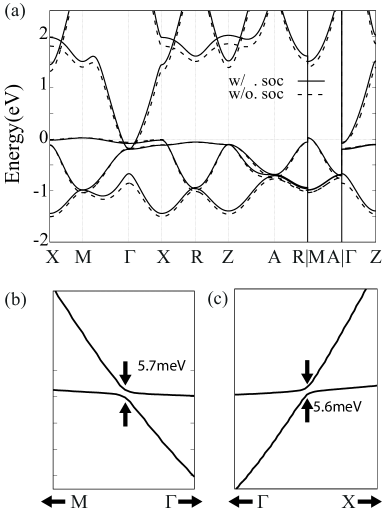
For the sake of completeness of the study, we calculate the electronic band structure of Na3N with SOC shown in Fig. S2(a). Indeed the effect of SOC is negligibly weak. It is found that SOC opens a tiny band gap along the entire DLN. As shown in Figs. S2(b) and (c), a band gap opens by 5.6 meV and 5.7 meV on the high-symmetry and lines, respectively. Considering SOC, strained Na3N can be considered as a strong topological insulator protected by time-reversal symmetry. We confirm the nontrivial topological insulator phase induced by SOC by calculating the invariants using parity eigenvalues. This calculation results in (1;000), indicating the strong topological insulator.
Appendix C: Parameters of the Hamiltonian
In Table S1, we present the parameters of the Hamiltonians for 1 %, 2 %, 3 %, and 4 %-strained Na3N, which best reproduce the corresponding first-principles band structures. These parameters were used to calculate the optical conductivities presented in Sec. VI.2.
| Parameters(eV) | 1 %-strained | 2 %-strained | 3 %-strained | 4 %-strained |
|---|---|---|---|---|
| 5.00 | 5.00 | 5.00 | 5.00 | |
| 4.60 | 4.60 | 4.60 | 4.60 | |
| 4.82 | 4.64 | 4.46 | 4.28 | |
| 4.46 | 4.32 | 4.18 | 4.04 | |
| 0.65 | 0.78 | 0.92 | 1.02 | |
| 0.070 | 0.095 | 0.109 | 0.125 |