Thin film of a topological insulator as a spin Hall insulator
Abstract
We study the spin conductivity of the surface states in a thin film of a topological insulator within Kubo formalism. Hybridization between the different sides of the film opens a gap at the Dirac point. We found that in the gapped region spin conductivity remains finite. In the gapless region near the band gap spin conductivity is enhanced. These findings make a thin film of a topological insulator as a promising material for spintronic applications.
pacs:
03.67.Lx, 74.90.+nI Introduction
Spin Hall effect - generation of the transverse spin current by the applied voltage - have been predicted in the materials with spin-orbit scattering Dyakonov and Perel (1971) and with strong spin-orbit interaction Murakami et al. (2003); Sinova et al. (2004). However, it has been shown that spin current in latter materials is small due to vertex corrections caused by point non-magnetic disorder Inoue et al. (2004); Raimondi and Schwab (2005), that is consistent with the experimental data Sinova et al. (2015).
While spin current is dissipationless itself Murakami et al. (2003), the accompanying charge current is dissipative. Ideal material for the spintronics should have high spin conductivity along with low charge conductivity. In fact, a finite spin current can be produced in the insulators, where the charge current is absent due to the band gap. Such effect is referred to quantum spin Hall effect (QSHE) and it is predicted in narrow gap semiconductors Murakami et al. (2004), graphene with enhanced spin-orbit interactions Kane and Mele (2005) and strained Rashba materials Bernevig and Zhang (2006). Also, QSHE is predicted in transition metal dichalcogenides, but for the experimentally relevant conditions spin Hall conductivity inside the gap does not occur Li et al. (2013).
Topological insulators have robust surface states that form Dirac cone due to topologically nontrivial band structure in the bulk Hasan and Kane (2010). Such materials have a potential in spintronics: record spin currents have been reported recently Mellnik et al. (2014); Fan et al. (2014); Wang et al. (2015); Fan et al. (2016); Khang et al. (2018). In a thin film finite hybridization between surface states open a gap at the Dirac point Lu et al. (2010); Shan et al. (2010). We argue that finite spin conductivity exists in the gapped region of such film.
In the previous paper, we study the bulk and surface spin conductivity of the thick topological insulators Akzyanov and Rakhmanov (2019). Also, spin conductivity in a thin film of a topological insulator is studied without taking into the account of the intralayer scattering and vertex corrections in Ref. Peng et al. (2016). The case of the gapped surface states due to intralayer hybridization has been missed. In this paper, we focus on the effects of the finite hybridization between the surface states in a thin film of a topological insulator.
We calculate the spin conductivity of the surface states of a thin film of topological insulator using Kubo formulas taking into account vertex corrections. We found that spin conductivity remains finite in a gapped region. Spin conductivity is enhanced near the gap in a metallic region. These finding can open the road for the application of thin films of topological insulators in low dissipative spintronics.
II Model
Low energy surface states in the thin film of topological insulator can be described by the Hamiltonian Liu et al. (2010); Lu et al. (2010); Shan et al. (2010) ()
| (1) | |||
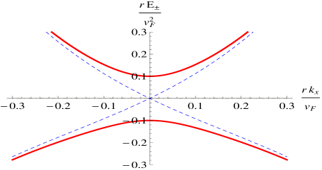
where are the Pauli matrices acting in the spin space, are the Pauli matrices acting in the layer space, is the chemical potential, is the Fermi velocity, is the inverse mass term, characterizes the next order correction to the Fermi velocity, and are the in-plane momentum components, is the value of the gap at the Dirac point due to hybridization of the surface states belong to different layers. The spectrum of the Hamiltonian (1) is doubly degenerate and is given by
| (2) |
If we measure the energy in terms of , then, the chemical potential, the next order correction to the Fermi velocity, and the gap are conveniently characterized by the dimensionless values , , and , respectively.
The spectrum forms a Dirac cone when the inverse mass term is small . In the opposite case, an additional Fermi surface with opposite helicity emerges for some values of chemical potential Akzyanov and Rakhmanov (2019). Note, that vanished inverse mass term leads to vanished spin conductivity.
In general, the spin conductivity can be presented as a sum of three terms Yang and Chang (2006); Kodderitzsch et al. (2015)
| (3) |
where the first two items correspond to a contribution from the states at the Fermi level and the third one from the filled states. Here and denote the in-plane coordinates and correspondingly, and denotes the spin projection.
At zero temperature and contribution of the states at the Fermi energy can be written as Inoue et al. (2004); Yang and Chang (2006)
| (4) | |||
| (5) |
Here , is the velocity operator, is the velocity operator with vertex corrections , means the anticommutator, and are the retarded and advanced disorder averaged Green functions, which will be specified later.
The contribution to the spin conductivity from the filled states
| (6) | |||
where is the Fermi distrubution function (that is Heaviside step for zero temperature), means complex conjugate.
III Disorder and vertex corrections
We will describe disorder by a potential , where is the Dirac delta function, are the positions of the randomly distributed point-like impurities with the local potential and concentration . We assume that the disorder is Gaussian, that is, and . We introduce disorder parameter as .
In the self-consistent Born approximation (SCBA), the impurity-averaged Green’s functions can be calculated as where are bare retarded/advanced Green’s functions of the Hamiltonian (1) and is the self-energy. Self-energy is defined as In the case under consideration, we can calculate the self-energy using an Dyson equation . The self-energy has nontrivial structure in the side space . Along with diagonal element it has non-diagonal one . Therefore, the expression for is similar to , in which is replaced by , by and by . The value describes diagonal scattering rate while describes non-diagonal scattering rate.
We start with the case of large chemical potential . In this case we can neglect a small correction to the value of due to real part of the self-energy and put . In this limit we suppose that scattering rates are small and we obtain that
Now we consider . In the metallic region we get that diagonal scattering rate is independent of chemical potential Kato et al. (2007)
| (7) |
Condition stands even for . Near the band gap we calculate scattering rates self-consistenly and found that scattering rates are exponentially suppressed for a weak disorder that is expected for the Dirac system Ostrovsky et al. (2006). In the insulating region condition Eq. 7 fails and non-diagonal scattering is always smaller than diagonal one .
The impurity averaged Green function can be calculated as or in the explicit form
| (8) |
In the SCBA, following the approach described in Ref. Shon and Ando (1998), we can derive an equation for the vertex corrected velocity operator Chiba et al. (2017)
| (9) |
IV Spin conductivity from the states at the Fermi surface
Now we use the obtained results and Eqs. (4) to calculate the contribution to the spin conductivity due to the states at the Fermi surface. On this way, we obtained, first, that in the considered approach the term vanishes exactly and we should compute the term only.
Isotropic tensor component is the only term that exists in the system. From Eq. (4) using condition we derive that
| (11) | |||
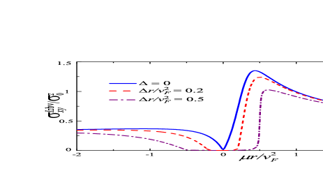
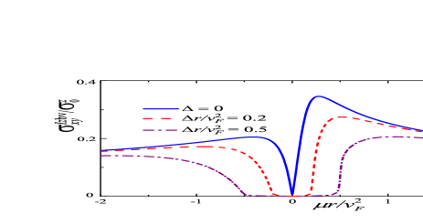
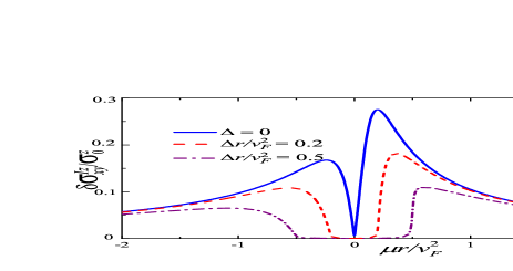
Here is the spin conductivity without vertex corrections, is the spin conductivity cotribution from the vertex corrections. We plot spin conductivity contributions as a function of the chemical potential for different values of the gap and correction to the Fermi velocity . We can see that spin conductivity contributions take maximal values near the gap .
V Spin conductivity from the filled states
We study Eq. 6 in a weak disorder limit. Isotropic component is the only term that exists in the system. After energy integration using constant damp apprxoimation for the we get that contribution to the spin conductivity from the filled states consists of two parts
| (12) |
where is the spin conductivity in a clean limit, is given by Eq. 11. Similar expression have been obtain for the anomalous charge Hall conductivity for the Dirac Hamiltonian Sinitsyn et al. (2007). Spin conductivity from the filled states in a clean limit can be expressed as Sinova et al. (2004); Sinitsyn et al. (2004)
| (13) |
Here is the energy of an electron in the -th band with the momentum , is the corresponding Bloch vector, , is the Fermi distribution function corresponding to (which is the Heaviside step-function in the considered case of zero temperature), Im is for the imaginary part, is the scalar product here. Using Eq. (13) we obtain
| (14) |
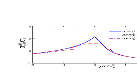
where is Heaviside step function and is the spin conductivity quanta. Finite disorder has a little impact on this term in the spin conductivity: Heaviside step function is replaced by the normalized arctangent function . This substitution leads to the insignificant blurring of the spin conductivity near the gap for a small disorder. Spin conductivity in a clean limit is shown on the Fig. 4 for different values the the gap and Fermi velocity correction . Spin conductivity is a constant in the gapped region and decreases in the gapless region. Also, its particle-hole asymmetry is controlled by the parameter : asymmetry is smaller for larger values of the parameter. We can see that spin conductivity in a gapped region is comparable to the spin conductivity in a metallic region near the gap , so at the Dirac point spin conductivity decreases with the increase of the gap .
VI Estimates for the experiment
We can extract information of the disorder from half-width of the quasiparticle peak in ARPES from Ref.Chen et al., 2013 and get . STM study shows that there is approximately 1 defect per for a clean surface Cheng et al. (2010). If we suppose that the typical impurity potential is is order of chemical potential cmeV (which is true for the vacation defects) and Fermi velocity for the surface states Zhang et al. (2009a) eV, then we get estimate for . Value of correction to the Fermi velocity for the surface states is extracted from the Ref. Rakyta et al., 2012, and we get where Nomura et al. (2014) eV. Hybridization between the layers depends strongly on the number of layers and reaches values of eV for two layers of Bi2Te3 Forster et al. (2016).
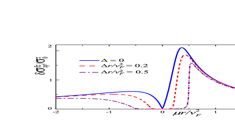
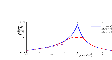
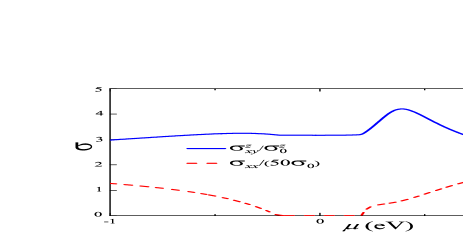
We can see from Eqs. 11 and 12 that the term cancels out from and . So, only contributions to the spin conductivity from the vertex corrections and spin conductivity in a clean limit remain. We plot total spin conductivity as a function of chemical potential for the experimentally relevant parameters. Spin conductivity remains finite inside the gap and is enhanced just outside of the gap. Also, it posses considerable particle-hole asymmetry. Charge conductivity is calculated by Proskurin et al. (2015) , where . Charge conductivity is suppressed inside the gap and it has a weak dependence of the value of chemical potential away from the gap as it is expected for the Dirac system Ostrovsky et al. (2006)
VII Discussion
Spin conductivity exists in a gapped region of a topological insulator thin film so this system is a spin Hall insulator. Spin conductivity is not changing inside the gap if we vary chemical potential. However, its value is not equal to the spin conductivity quanta because Hamiltonian does not commute with the z-component of the spin Dayi and Yunt (2015), so spin is not conserved. It differs our system from the spin Hall insulators that have been considered before Murakami et al. (2004); Kane and Mele (2005); Bernevig and Zhang (2006); Li et al. (2013). In a similar way charge quantum Hall conductivity is not quantized in superconductors since charge is not conserved in such materials Bednik et al. (2016).
In the Kane-Mele like models, where spin is conserved , spin conductivity is generated by the spinful interaction between the Dirac cones Kane and Mele (2005); Li et al. (2013). In our model interaction between the Dirac cones is independent of the spin and spin conductivity is generated by the intrinsic spin-orbit coupling as it is expected for the Rashba systems Sinova et al. (2004).
We suppose that both sides of the film are identical. In real samples asymmetry between different sides of the film can arise due to different doping and concentration of the defects. In a weak scattering limit, different scattering on the different sides of the film has almost no influence on the total spin conductivity if vertex corrections are neglected. However, significant asymmetry between the layers can have an effect on the vertex corrections.
Hybridization between layers, given by , couples electron (hole) from the Dirac cone of one layer to the hole (electron) of Dirac cone of another layer with the same spin. Such a bound state does not carry a charge but carries double spin and has spin-momentum locking of the parent electron. If we apply the electric field, then the flow of such bound states with zero charges will produce spin current without the generation of the electric current.
The region inside the gap is of special interest. Scattering and dissipation are strongly suppressed due to an absence of the states at the Fermi energy. However, finite spin conductivity is present. Such a phase can be promising for low dissipation spintronics applications.
Outside the gap spin conductivity is enhanced due to presence of the contribution of the states at the Fermi energy. This enhancement is significant only for a thin films . If there are several layers then the gap is significantly suppressed in comparison with the mass parameter eV. For the 4 layer film, bandgap reaches a value of meV and is almost vanished for thicker samples Forster et al. (2016). Thus, the effect of the enhancement of spin conductivity is significant only in a few layers samples.
Experimentally, the dissipationless spin current can be measured by the spin-transfer torque effect Ralph and Stiles (2008); Sinova et al. (2015). If we apply voltage, then magnetization of the magnetic layer on the top of the topological insulator can be changed by the spin current without the generation of the electrical current. Thus, the ratio of spin current to charge current - spin Hall angle - would be extremely large for such a system. However, the magnetic layer on the top should be an insulator to prevent shunting.
We do not consider the influence of the magnetic field on the spin conductivity. In the real experiments on spin-transfer torque magnetic layers are used. Thus, the magnetization of the magnetic layer affects the value of the spin conductivity of the topological insulator. However, if magnetization is small (value of the Zeeman splitting is much smaller then chemical potential ) then its influence on the spin conductivity can be neglected.
Experiments on spin-transfer torque in a film of topological insulators with eight layers have been performed Mellnik et al. (2014). Good quality ultrathin films of topological insulators with a few layers are availableZhang et al. (2009b); Kim et al. (2013). The gap for the surface states is about 180 meV for the four-layer samples Lang et al. (2013). So, the measure of spin current in a thin layer topological insulator inside and near the gap is as an experimentally achievable task.
To sum up, hybridization between the surface states in different layers of a thin film of a topological insulator opens a gap near the Dirac point. We found that finite spin conductivity exists in the gapped region. In a metallic region near the gap, spin conductivity is enhanced. These findings can be crucial towards the implementation of thin films of topological insulators in low-dissipation spintronics.
Acknowledgements
We acknowledge support from the Russian Science Foundation, Grant No 17-12-01544, RFBR according to the research project № 19-32-80014, Foundation for the Advancement of Theoretical Physics and Mathematics “BASIS”.
References
- Dyakonov and Perel (1971) M. Dyakonov and V. Perel, “Current-induced spin orientation of electrons in semiconductors,” Physics Letters A 35, 459 (1971).
- Murakami et al. (2003) S. Murakami, N. Nagaosa, and S.-C. Zhang, “Dissipationless Quantum Spin Current at Room Temperature,” Science 301, 1348 (2003).
- Sinova et al. (2004) J. Sinova, D. Culcer, Q. Niu, N. A. Sinitsyn, T. Jungwirth, and A. H. MacDonald, “Universal Intrinsic Spin Hall Effect,” Phys. Rev. Lett. 92, 126603 (2004).
- Inoue et al. (2004) J.-i. Inoue, G. E. W. Bauer, and L. W. Molenkamp, “Suppression of the persistent spin Hall current by defect scattering,” Phys. Rev. B 70, 041303 (2004).
- Raimondi and Schwab (2005) R. Raimondi and P. Schwab, “Spin-Hall effect in a disordered two-dimensional electron system,” Phys. Rev. B 71, 033311 (2005).
- Sinova et al. (2015) J. Sinova, S. O. Valenzuela, J. Wunderlich, C. Back, and T. Jungwirth, “Spin Hall effects,” Rev. Mod. Phys. 87, 1213 (2015).
- Murakami et al. (2004) S. Murakami, N. Nagaosa, and S.-C. Zhang, “Spin-Hall Insulator,” Phys. Rev. Lett. 93, 156804 (2004).
- Kane and Mele (2005) C. L. Kane and E. J. Mele, “Quantum Spin Hall Effect in Graphene,” Phys. Rev. Lett. 95, 226801 (2005).
- Bernevig and Zhang (2006) B. A. Bernevig and S.-C. Zhang, “Quantum Spin Hall Effect,” Phys. Rev. Lett. 96, 106802 (2006).
- Li et al. (2013) X. Li, F. Zhang, and Q. Niu, “Unconventional Quantum Hall Effect and Tunable Spin Hall Effect in Dirac Materials: Application to an Isolated Trilayer,” Phys. Rev. Lett. 110, 066803 (2013).
- Hasan and Kane (2010) M. Z. Hasan and C. L. Kane, “Colloquium,” Rev. Mod. Phys. 82, 3045 (2010).
- Mellnik et al. (2014) A. R. Mellnik, J. S. Lee, A. Richardella, J. L. Grab, P. J. Mintun, M. H. Fischer, A. Vaezi, A. Manchon, E.-A. Kim, N. Samarth, et al., “Spin-transfer torque generated by a topological insulator,” Nature 511, 449 (2014).
- Fan et al. (2014) Y. Fan, P. Upadhyaya, X. Kou, M. Lang, S. Takei, Z. Wang, J. Tang, L. He, L.-T. Chang, M. Montazeri, et al., “Magnetization switching through giant spin-orbit torque in a magnetically doped topological insulator heterostructure,” Nat Mater 13, 699 (2014).
- Wang et al. (2015) Y. Wang, P. Deorani, K. Banerjee, N. Koirala, M. Brahlek, S. Oh, and H. Yang, “Topological Surface States Originated Spin-Orbit Torques in ,” Phys. Rev. Lett. 114, 257202 (2015).
- Fan et al. (2016) Y. Fan, X. Kou, P. Upadhyaya, Q. Shao, L. Pan, M. Lang, X. Che, J. Tang, M. Montazeri, K. Murata, et al., “Electric-field control of spin-orbit torque in a magnetically doped topological insulator,” Nat Nano 11, 352 (2016).
- Khang et al. (2018) N. H. D. Khang, Y. Ueda, and P. N. Hai, “A conductive topological insulator with large spin Hall effect for ultralow power spin-orbit torque switching,” Nature Materials 17, 808 (2018).
- Lu et al. (2010) H.-Z. Lu, W.-Y. Shan, W. Yao, Q. Niu, and S.-Q. Shen, “Massive Dirac fermions and spin physics in an ultrathin film of topological insulator,” Phys. Rev. B 81, 115407 (2010).
- Shan et al. (2010) W.-Y. Shan, H.-Z. Lu, and S.-Q. Shen, “Effective continuous model for surface states and thin films of three-dimensional topological insulators,” New Journal of Physics 12, 043048 (2010).
- Akzyanov and Rakhmanov (2019) R. S. Akzyanov and A. L. Rakhmanov, “Bulk and surface spin conductivity in topological insulators with hexagonal warping,” Phys. Rev. B 99, 045436 (2019).
- Peng et al. (2016) X. Peng, Y. Yang, R. R. Singh, S. Y. Savrasov, and D. Yu, “Spin generation via bulk spin current in three-dimensional topological insulators,” Nature Communications 7, 10878 (2016).
- Liu et al. (2010) C.-X. Liu, X.-L. Qi, H. Zhang, X. Dai, Z. Fang, and S.-C. Zhang, “Model Hamiltonian for topological insulators,” Phys. Rev. B 82, 045122 (2010).
- Yang and Chang (2006) M.-F. Yang and M.-C. Chang, “Středa-like formula in the spin Hall effect,” Phys. Rev. B 73, 073304 (2006).
- Kodderitzsch et al. (2015) D. Kodderitzsch, K. Chadova, and H. Ebert, “Linear response Kubo-Bastin formalism with application to the anomalous and spin Hall effects: A first-principles approach,” Phys. Rev. B 92, 184415 (2015).
- Kato et al. (2007) T. Kato, Y. Ishikawa, H. Itoh, and J. ichiro Inoue, “Anomalous Hall effect in spin-polarized two-dimensional electron gases with Rashba spin-orbit interaction,” New Journal of Physics 9, 350 (2007).
- Ostrovsky et al. (2006) P. M. Ostrovsky, I. V. Gornyi, and A. D. Mirlin, “Electron transport in disordered graphene,” Phys. Rev. B 74, 235443 (2006).
- Shon and Ando (1998) N. Shon and T. Ando, “Quantum Transport in Two-Dimensional Graphite System,” J. Phys. Soc. Jpn. 67, 2421 (1998).
- Chiba et al. (2017) T. Chiba, S. Takahashi, and G. E. W. Bauer, “Magnetic-proximity-induced magnetoresistance on topological insulators,” Phys. Rev. B 95, 094428 (2017).
- Sinitsyn et al. (2007) N. A. Sinitsyn, A. H. MacDonald, T. Jungwirth, V. K. Dugaev, and J. Sinova, “Anomalous Hall effect in a two-dimensional Dirac band: The link between the Kubo-Streda formula and the semiclassical Boltzmann equation approach,” Phys. Rev. B 75, 045315 (2007).
- Sinitsyn et al. (2004) N. A. Sinitsyn, E. M. Hankiewicz, W. Teizer, and J. Sinova, “Spin Hall and spin-diagonal conductivity in the presence of Rashba and Dresselhaus spin-orbit coupling,” Phys. Rev. B 70, 081312 (2004).
- Chen et al. (2013) C. Chen, Z. Xie, Y. Feng, H. Yi, A. Liang, S. He, D. Mou, J. He, Y. Peng, X. Liu, et al., “Tunable Dirac Fermion Dynamics in Topological Insulators,” Scientific Reports 3, 2411 (2013).
- Cheng et al. (2010) P. Cheng, C. Song, T. Zhang, Y. Zhang, Y. Wang, J.-F. Jia, J. Wang, Y. Wang, B.-F. Zhu, X. Chen, et al., “Landau Quantization of Topological Surface States in ,” Phys. Rev. Lett. 105, 076801 (2010).
- Zhang et al. (2009a) H. Zhang, C.-X. Liu, X.-L. Qi, X. Dai, Z. Fang, and S.-C. Zhang, “Topological insulators in Bi2Se3, Bi2Te3 and Sb2Te3 with a single Dirac cone on the surface,” Nat Phys 5, 438 (2009a).
- Rakyta et al. (2012) P. Rakyta, A. Pályi, and J. Cserti, “Electronic standing waves on the surface of the topological insulator Bi2Te3,” Phys. Rev. B 86, 085456 (2012).
- Nomura et al. (2014) M. Nomura, S. Souma, A. Takayama, T. Sato, T. Takahashi, K. Eto, K. Segawa, and Y. Ando, “Relationship between Fermi surface warping and out-of-plane spin polarization in topological insulators: A view from spin- and angle-resolved photoemission,” Phys. Rev. B 89, 045134 (2014).
- Forster et al. (2016) T. Forster, P. Krüger, and M. Rohlfing, “ calculations for and thin films: Electronic and topological properties,” Phys. Rev. B 93, 205442 (2016).
- Proskurin et al. (2015) I. Proskurin, M. Ogata, and Y. Suzumura, “Longitudinal conductivity of massless fermions with tilted Dirac cone in magnetic field,” Phys. Rev. B 91, 195413 (2015).
- Dayi and Yunt (2015) O. F. Dayi and E. Yunt, “Relation between the spin Hall conductivity and the spin Chern number for Dirac-like systems,” Int. J. Geom. Methods Mod. Phys. 13, 1550136 (2015).
- Bednik et al. (2016) G. Bednik, A. A. Zyuzin, and A. A. Burkov, “Anomalous Hall effect in Weyl superconductors,” New Journal of Physics 18, 085002 (2016).
- Ralph and Stiles (2008) D. Ralph and M. Stiles, “Spin transfer torques,” Journal of Magnetism and Magnetic Materials 320, 1190 (2008).
- Zhang et al. (2009b) G. Zhang, H. Qin, J. Teng, J. Guo, Q. Guo, X. Dai, Z. Fang, and K. Wu, “Quintuple-layer epitaxy of thin films of topological insulator Bi2Se3,” Appl. Phys. Lett. 95, 053114 (2009b).
- Kim et al. (2013) D. Kim, P. Syers, N. P. Butch, J. Paglione, and M. S. Fuhrer, “Coherent topological transport on the surface of Bi2Se3,” Nature Communications 4, 2040 (2013).
- Lang et al. (2013) M. Lang, L. He, X. Kou, P. Upadhyaya, Y. Fan, H. Chu, Y. Jiang, J. H. Bardarson, W. Jiang, E. S. Choi, et al., “Competing Weak Localization and Weak Antilocalization in Ultrathin Topological Insulators,” Nano Lett. 13, 48 (2013).