Strongly inhomogeneous distribution of spectral properties of silicon-vacancy color centers in nanodiamonds
Abstract
The silicon-vacancy (SiV) color center in diamond is a solid-state single photon emitter and spin quantum bit suited as a component in quantum devices. Here, we show that the SiV center in nanodiamond exhibits a strongly inhomogeneous distribution with regard to the center wavelengths and linewidths of the zero-phonon-line (ZPL) emission at room temperature. We find that the SiV centers separate in two clusters: one group exhibits ZPLs with center wavelengths within a narrow range and broad linewidths between , whereas the second group comprises a very broad distribution of center wavelengths between , but narrow linewidths from below up to . Supported by ab initio Kohn-Sham density functional theory calculations we show that the ZPL shifts of the first group are consistently explained by strain in the diamond lattice. Further, we suggest, that the second group showing the strongly inhomogeneous distribution of center wavelengths might be comprised of modified SiV centers. Whereas single photon emission is demonstrated for SiV centers of both clusters, we show that emitters from different clusters show different spectroscopic features such as variations of the phonon sideband spectra and different blinking dynamics.
1 Introduction
Recently, the negatively charged silicon-vacancy center (SiV center) has received growing interest in the fields of quantum communication and quantum information due to its favorable spectral properties and optically accessible spin states [1, 2, 3, 4].
In particular, SiV centers in low strain bulk diamond have been shown to exhibit close to Fourier-limited linewidths [5, 6, 7] and emission of indistinguishable photons [8] from two distinct emitters, a prerequisite for many applications in quantum technologies [9].
As the spin coherence time of SiV centers in bulk diamond is limited by phonon-induced decoherence processes down to liquid-Helium temperatures [1, 3, 10], diamond nanostructures or nanodiamonds might provide an advantage based on phonon confinement effects modifying the phonon density of states.
Additionally, some applications require diamonds of the size of a few ten nanometers.
Examples include applications as fluorescence markers [11, 12] or the implementation of SiV centers in photonic structures such as microcavities [13, 14] or optical antennas [15, 16].
In light of such applications, nanodiamonds hosting color centers provide a significant advantage:
Suitable SiV centers can be spectroscopically preselected according to desired properties and can then be relocated to be used in the target structure using pick-and-place techniques [17].
Previous research demonstrated the production of nanodiamonds including SiV centers produced by chemical vapor deposition (CVD) [18], high-pressure, high-temperature (HPHT) [19] and bead-assisted sonic disintegration (BASD) [20] processes.
Although several studies [21, 22] have indicated nearly Fourier-limited linewidths of SiV centers in nanodiamonds, in general the spectral properties of SiV centers are strongly dependent on strain in the diamond lattice [23, 24, 25].
In this study we investigate the properties of SiV centers in nanodiamonds of sizes of produced in a wet-milling process in a vibrational mill.
Starting material was a CVD grown diamond film with in-situ incorporated SiV defects.
The advantage of wet-milled nanodiamonds with in-situ incorporated SiV centers lies in its high production rate of nanodiamonds, yielding a perfect candidate for preselection of spectral properties and consecutive implementation in target applications.
The fluorescence spectra of the SiV centers show that both the center wavelength of the ZPL as well as the linewidth of the zero-phonon-line vary strongly among different diamonds.
Our measurements show a strong correlation between the center wavelength of the zero-phonon-line and the corresponding linewidths, resulting in a previously unreported bimodal distribution.
We find single photon emission from these SiV centers over the whole range of zero-phonon-line positions and linewidths, although with a large variation in photon emission rate and fluorescence stability.
2 Methods
2.1 Nanodiamond Production
In the following, we describe the processes used to produce nanodiamond samples of interest. We deploy two different methods of incorporating SiV centers into wet-milled nanodiamonds: Incorporation during (in-situ), and implanting after the diamond growth process. The obtained samples are prefixed in-situ and implanted respectively, see Table 1 for an overview of the available samples.
| Sample name | Diameter | Siv incorporation | post-processing | |||
|---|---|---|---|---|---|---|
| insitu50 | in-situ |
|
||||
| insitu70 | in-situ |
|
||||
| insitu70n | in-situ |
|
||||
| insitu70o | in-situ |
|
||||
| insitu100 | in-situ |
|
||||
| insitu100ao | in-situ |
|
||||
| implanted250ao | implanted |
|
The starting material for the wet-milled nanodiamonds was a nanocrystalline diamond film [26], directly grown on a silicon wafer using chemical vapor deposition (CVD).
A microwave hydrogen plasma containing 1% methane was used to grow on purified nanodiamond seeds (produced by PlasmaChem).
To induce in-situ SiV center creation, sacrificial silicon pieces are situated in the growth chamber.
During diamond growth the silicon pieces are etched by the plasma and individual silicon atoms are incorporated into the diamond lattice.
Using a wet-milling process, the diamond film after removal of the substrate is milled with steel beads in a vibrational mill.
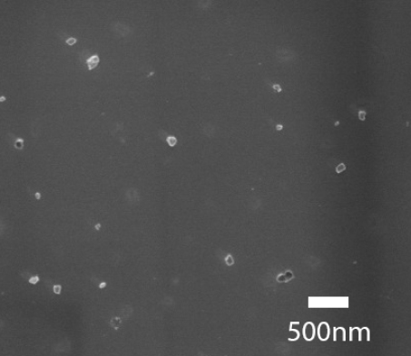
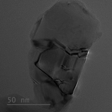
The resulting particle suspension is fractionated using centrifugation, leading to diamond particles of a size of about in average diameter (Figure 1(a)), as determined with dynamic light scattering. Transmission Electron Microscopy (TEM) graphs of the milled diamond particles show that the nanodiamonds are polycrystalline and exhibit typical single-crystal sizes of a few tens of nanometers.
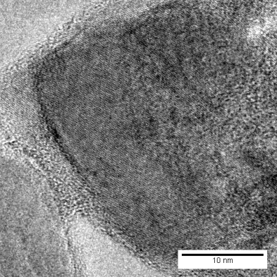
In Figures 1(b) and 1(c) TEM images of a typical nanodiamond are shown. Within the nanodiamond, several sharp lines are visible.
These lines are edges of crystal boundaries and grain boundaries, introducing strain in the diamond lattice.
We remark at this point that some studies suggest the possibility that SiV centers are created with a higher probability at grain boundaries and morphological defects than within the core of the crystal [27, 28].
The high amount of debris from milling beads is removed for the most part by extensive acid treatment and the absence of debris shown by spectroscopic characterisation.
We also explored milling nanodiamonds with silicon nitride beads, and found that the choice of bead material did not cause any noticeable spectroscopic difference.
The aqueous solution containing the nanodiamonds is drop-cast onto an iridium film on a silicon substrate.
The iridium film is grown onto a buffer layer of yttria-stabilized zirconia (YSL), which in turn is grown onto a silicon wafer.
The iridium surface has the advantage that it acts as an antenna enhancing the collection efficiency of fluorescence light [29].
Prior to drop-casting, the substracte was cleaned using Piranha solution (50% sulfuric acid H2SO4, 50% hydrogen peroxide H2O2).
This enhances surface hydrophilicity, leading to a homogeneous distribution of the diamond particles on the substrate.
Post-processing treatment is comprised of annealing in vacuum at , consecutive oxidation in air at a temperature of or a combination thereof.
The duration for either treatment method was 3-6 hours.
As mentioned before, we also investigated nanodiamonds with SiV centers implanted after completed diamond growth.
As starting material we used a polycrystalline diamond film (Element Six, electronic grade) for which we verified that it did not contain SiV centers initially.
In bulk material, the implantation causes the SiV centers to form in a specific depth dependent on the implantation energy, leaving most of the diamond vacant of SiV centers.
As a consequence, a significant portion of nanodiamonds milled from such a bulk material would not host any SiV centers.
To obtain diamond particles with a homogeneous distribution of SiV centers, the following steps were taken:
First, the diamond film was milled to diamond particles of sizes on the order of a few micrometers.
In a second step, these microdiamonds were densely spin-coated onto iridium substrates and implanted with silicon (implantation energy , fluence ).
To eliminate damage from the implantation process, the diamonds were annealed in vacuum at and subsequently oxidized in air at for 3 hours each.
At this stage, we verified successful creation of SiV centers via optical spectroscopy.
Finally, the micrometer sized diamond particles were milled to a size of .
2.2 Experimental Setup
We obtained photoluminescence spectra and photon statistics of the samples using a home-built confocal microscope. For excitation we use a continuous wave diode laser (Schäfter-Kirchhoff, 58FCM) at . The excitation laser is focused onto the sample via a microscope objective with a numerical aperture of 0.8 (Olympus, LMPlanFLN 100x), which also collects the fluorescence light emitted from the sample. Both the laser light reflected by the sample and the fluorescence light pass through a glass plate used to couple the excitation laser into the microscope objective. The residual laser light is then filtered out by two longpass filters. The emission light is coupled into a single mode fiber which serves as pinhole in the confocal setup. The emission is either guided to a grating spectrometer or to two single photon detectors (PicoQuant, tau-SPAD-100) used in a HBT configuration to measure photon statistics. In front of the avalanche photo diodes bandpass filters select the spectral window in which the investigated color centers emit photons. These filters are chosen according to each individual emitter: Due to strong shifts in the zero-phonon-line wavelength, we use different bandpass filters in front of the APDs to suppress background fluorescence and effectively select the luminescence of the zero-phonon-line.
3 Results
In the following, we present our findings regarding diamond crystal characteristics and spectroscopic measurement of SiV centers. Unless explicitly stated, we rely on measurements of milled nanodiamonds containing in-situ incorporated SiV centers, i.e. samples insitu50, insitu70, and insitu100 as listed in Table 1.
3.1 Diamond Crystal Quality
We aim to perform spectroscopic measurements of single SiV centers in wet-milled nanodiamonds.
To this end, we focus on producing pristine wet-milled diamond nanoparticles containing a single SiV center each.
Raman measurements of the nanodiamonds allow us to identify issues with surface contamination, defects of the diamond lattice, and strain in the diamond lattice [30, 31, 32].
Surface contamination like graphite and amorphous sp2 hybridized carbon manifest themselves as additional peaks in the Raman spectrum.
Strain in the diamond lattice broadens the first order Raman peak and causes it to shift to higher or smaller wavenumbers.
Similarly, high concentrations of lattice defects cause additional peaks, a broadening of the first order Raman peak and a shift towards smaller wavenumbers.
The size of single nanodiamonds is on the order of tens of nanometers, thus low signal intensities can become an issue.
To overcome this problem we pursue two different approaches to perform Raman measurements:
-
a)
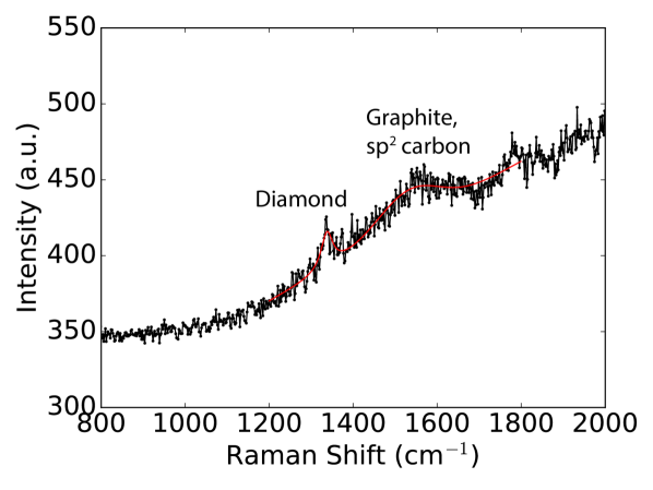
Nanodiamond clusters: Collective measurements are carried out at several areas on the sample insitu70. Since this sample is densely covered with nanodiamonds, collective measurements of clusters of nanodiamonds (Figure 2(a)) achieves higher signal intensities.
-
b)
Large nanodiamonds: Raman measurements are carried out on the implanted sample implanted250ao. For this sample, diamond particles are large enough to yield sufficient intensities on single nanodiamonds.
For all Raman measurements a continuous wave diode laser was used for excitation.
Surface Contamination
We test the impact of oxidation treatment as described in Section 2 on surface contamination.
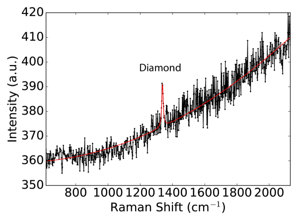
Figure 2(a) shows a measured Raman spectrum of a sample without oxidation treatment (insitu70n).
To verify reproducibility, the measurement is performed on three different spots of the sample.
The narrow peak in Figure 2(a) corresponds to the first order diamond Raman peak and will be further analyzed in below.
The spectrum also shows a broad peak with a Raman shift of about .
This shift corresponds to the G-band due to amorphous sp2 hybridized carbon atoms and graphite.
The exact G-band position and linewidth is sensitive to parameters such as the clustering of the sp2 phase, bond-length and bond-angle disorder, presence of sp2 rings or chains, and the sp2/sp3 ratio [33].
The nanodiamond Raman spectra are considerably modified after oxidation in air at .
To verify this, we perform Raman measurements on three different spots of a sample produced in the same process as the above mentioned, which is additionally oxidized (insitu70o).
While the G-band peak is present in every measurement performed on a non-oxidized sample, it is not present in any of the oxidized samples (Figure 2(b)), indicating successful removal of a majority of sp2 hybridized carbon and surface graphite.
Defect Concentration
Several effects impact the first order diamond Raman line:
1. defects in the diamond lattice,
2. hydrostatic pressure,
3. uniaxial or more complicated stress configurations.
In the measurement on nanodiamond clusters the width of the diamond Raman peak of sample insitu70 varies between without oxidation treatment, but is only after the oxidation process.
A possible reason for this change of the width is improved crystal quality [20, 31].
In the measurement on large nanodiamonds we measured a Raman line at (denoted line R1) which exhibits a broad linewidth of .
One plausible explanation for both the position and the linewidth of the Raman line are defects in the diamond lattice[31].
Strain
We investigated how strain in the diamond lattice manifests itself in both measurements on nanodiamond clusters and on large nanodiamonds.
In the Raman measurement on nanodiamond clusters, the position of the diamond Raman peak is the same for oxidized (insitu70o) and non-oxidized (insitu70n) samples, indicating that oxidation does not affect strain in the diamond.
However, the Raman shift of both non-oxidized and oxidized samples amounts to , as compared to the literature value of of pristine diamond [30] (given uncertainties are governed by spectrometer resolution).
This shift indicates the presence of strain in the diamond particles.
Performing the Raman measurement on large nanodiamonds we find diamond Raman lines between (line R1) and (line R2), indicating a broad distribution of strain among the individual diamond particles (uncertainties governed by spectrometer resolution).
Only line R1 could be explained with a high defect concentration in the diamond lattice due to its shift to smaller wavelengths.
However, a more consistent model which explains all occurring shifts is the presence of strain/stress in the diamond nanoparticles.
The Raman shift in the presence of compressive and tensile stress is given by [34, 35]: , where the Raman shift is given in cm-1 and the stress in GPa.
The calculation yields a pressure range from tensile stress to compressive stress.
Whereas under hydrostatic pressure the triply degenerate first order Raman peak remains degenerate, under uniaxial and more complex stress configurations (biaxial stress, shear stress etc.) mode splitting occurs [31].
As mentioned above, we observe broad linewidths up to .
The broad Raman linewidths may be attributed to uniaxial strain where mode splitting manifests itself in a broadening of the peak due to limited spectrometer resolution.
3.2 Photoluminescence spectra
To identify nanodiamonds containing SiV centers, we performed confocal scans of the samples. To reduce bias in the measurements, not only the brightest spots of the confocal scans are investigated, but also those which barely exceed background fluorescence. SiV centers are further investigated by measuring photoluminescence (PL) spectra, single photon statistics and photostability. The typical luminescence spectrum of an SiV center is composed of a prominent zero-phonon-line and weak sidebands. Investigations of both are reported independently in the following paragraphs.
3.2.1 Zero-phonon-line
ZPL distribution
The center wavelength and the linewidth of the zero-phonon-line (ZPL) of SiV luminescence spectra for samples insitu50, insitu70, and insitu100 are determined by fitting a Lorentzian fit to the ZPL.
Both spectra from single and multiple SiV centers are taken into account.
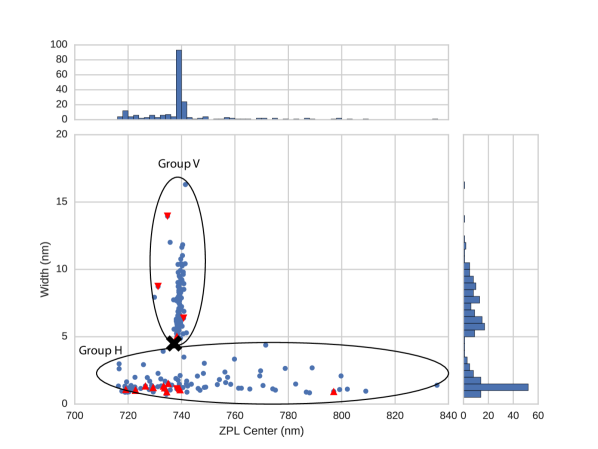
In Figure 3 the linewidth for each measured ZPL is plotted against its center wavelength.
What immediately strikes the eye is a pattern that to our knowledge has not been reported to date:
The observed ZPLs partition into two groups, here denoted as horizontal cluster (group H) and a vertical cluster (group V). The two distributions are seperated by a gap, i.e. a region with a pronounced lack of data points.
Single emitters are found both in group H and group V, marked as red triangles in Figure 3. Further details on single emitters are given in section 3.3.
The two groups are defined by their characteristic center wavelengths and linewidths:
In group H very prominent ZPL peaks are found showing linewidths in the range of and center wavelengths in the range of .
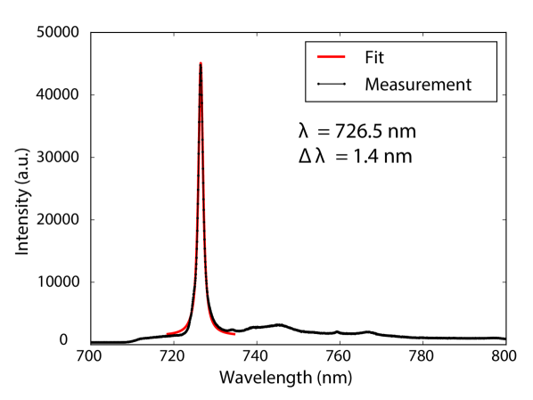
Figure 4(a) shows a representative spectrum of a single emitter in group H (denoted emitter H1), exhibiting a ZPL linewidth of and a center wavelength of .
In contrast, in group V the spectra exhibit broader ZPL linewidths of approximately up to .
Their ZPL center wavelengths, however, are distributed within the very narrow range of .
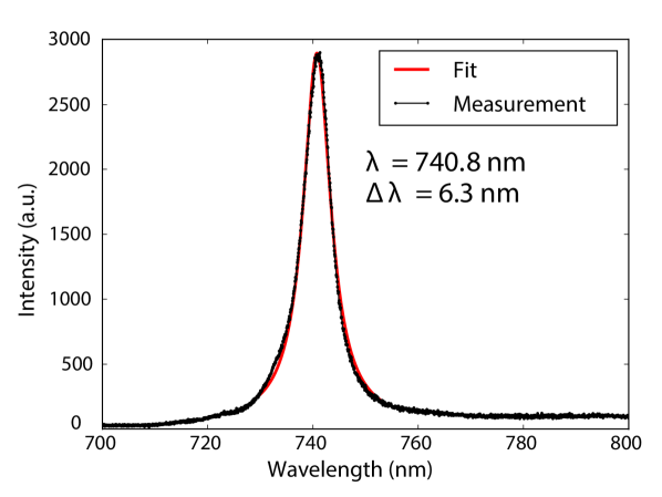
Figure 4(b) shows a spectrum of a single emitter of group V (denoted emitter V1) with a ZPL linewidth of and a center wavelength of .
For comparison, the room temperature ZPL of SiV centers in unstrained bulk diamond exhibits a linewidth of and a center wavelength of marked with a black cross in Figure 3 [6, 36].
Debye-Waller factor
To determine how much the ZPLs contribute to the total observed emission of emitter H1 and emitter V1, we determine the Debye-Waller factor defined as where and are intensities in ZPL and total spectrum, respectively.
The Debye-Waller factor for emitter H1 amounts to (given uncertainty due to fit).
This Debye-Waller factor corresponds to a Huang-Rhys factor [37] of , which is in good agreement with the values reported in [18].
The error is mainly due to background corrections.
When zooming in onto the spectrum of emitter V1 we do not find distinct sidebands peaks, i.e. almost all emission for this emitter is contained within the ZPL.
Considering resolution limits of the spectrometer, darkcounts and fluorescence background, we evaluate the Debye-Waller factor to be larger than which is the largest Debye-Waller factor among all investigated SiV centers.
The two Debye-Waller factors discussed here should not be interpreted as representative for the respective groups, they rather demonstrate the spread of the Debye-Waller factors of both groups.
It has to be pointed out that we did not find any systematic difference of the Debye-Waller factor between group H and group V.
Comparison to earlier results
To provide context for the novel findings presented in Figure 3, we compare our results to various earlier findings. Furthermore, we discuss an additional comparison to an investigated control sample fabricated using silicon implantation. The results are presented in Figure 5.
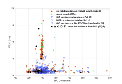
Samples for which previous data has been taken are:
- 1.
- 2.
- 3.
All previous data from different nanodiamond material fit nicely with the ZPL distribution presented in Figure 3(a), confirming the findings of Figure 3.
We verify that the observed luminescent centers are indeed silicon-related defects by performing control experiments with silicon implanted samples (sample implanted250ao).
By doing so we rule out the possibility that the two clusters in the distribution are a result of artifacts.
Such artifacts include other elements incorporated into the nanodiamonds during the growth process: Residue from previous processes performed in the diamond growth chamber or material from chamber parts may be incorporated during nanodiamond growth.
Figure 5 shows that the implanted SiV centers cover the same spectral range from around as the in-situ incorporated centers.
This correlation provides strong evidence for the silicon related origin of the defects.
Discussion of ZPL strain shift
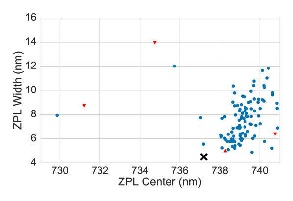
To provide a theoretical interpretation, the ZPL center wavelength shift is investigated in further detail and compared to results from density functional theory calculations: Zooming in to group V (Figure 3(c)) it becomes clear that only six of the measured data points in group V are situated at a shorter center wavelength than the point attributed to an ideal SiV center in unstrained bulk material, the shortest wavelength ZPL being situated at . At the same time, much more data exhibit a center wavelength red-shifted to the ideal SiV center. This asymmetry suggests that a red-shift of the ZPL of an SiV center is significantly more likely than a blueshift. Several mechanisms contribute to the center wavelength shift, predominantly hydrostatic and uniaxial strain. As discussed in Section 3.1, we estimate the stress in our nanodiamond sample from Raman measurements to be on the order of . In the following, we first discuss the stress/strain shift mechanisms for the SiV center before we compare theoretically derived strain shift coefficients to the mentioned range of ZPL shifts.
Computational method
To gain insight into the strain mechanism for the SiV centers in diamond, we perform ab initio Kohn-Sham density functional theory (DFT) calculations on the strain ZPL shift coupling parameters. The unstrained model of the negatively charged silicon vacancy defect (SiV-) in bulk diamond is constructed starting from a 512 atom pristine diamond simple cubic supercell within the point approximation. The point sampling of the Brillouin zone has proven to be adequate for defects in 512-atom supercells [39, 40] providing a sufficiently converged charge density. The SiV- defect has S= and it is found to have symmetry with an axis oriented along . Standard projector augmented-wave (PAW) formalism together with plane waves are applied, as implemented in the Vienna Ab-initio Simulation Package (VASP) code [41, 42, 43, 44]. The geometry optimization is carried out within the constructed supercell by using the Perdew-Burke-Ernzerhof (PBE) [45] DFT functional. A eV cutoff is applied for the wave function expansion and a eV cutoff for the charge density. The geometry of the defect is optimized until the forces were lower than eV/Å-1. The symmetry is preserved for both the ground state and the excited state after relaxation.
The ground state of the defect is found to have electronic configuration () while the excited state is modeled by promoting one electron from the to the level and presents electronic configuration (). Both these states are dynamic Jahn-Teller systems [46, 47]. The optical signal of the defect (ZPL) can be calculated as the lowest excitation energy by the constraint DFT approach (CDFT) [48]. According to CDFT one electron is promoted from the ground state to a higher level leaving a hole behind. The interaction between the electron and the hole is included in the procedure. The ZPL energies were obtained by taking the total energies of the optimized geometries in the ground and excited state.
The strain on the defect structure is simulated by applying a compression to the supercell along a well defined direction. The strained supercells are obtained by compressions along , and . We also study the configuration produced by a hydrostatic pressure, which consists in subjecting the cell to the same compression along the three directions. After introducing the strain along the directions, the ZPL energies were calculated for each strained supercell. Finally, we obtained data points on the calculated ZPL energies vs. the applied strain. These ZPL energies correspond to the optical transition between the lower branch levels of the and doublets. We note that additional calculations were performed for the and strained supercells by using the screened, range-separated, non-local hybrid density functional of Heyd-Scuseria-Ernzerhof (HSE06) [49, 50] and we found good agreement with the PBE values.
Nudged elastic band (NEB) calculations [51] by HSE06 were performed in order to calculate the energy barriers in the ground state in strained supercells. The barrier energies between the configurations stayed under 10.0 meV which implies small change in the adiabatic potential energy surface around the symmetry upon the applied strain. As a consequence, the Ham reduction factor in strained SiV center will minutely change with respect to that of unstrained SiV center [52]. This suggests that the observed ZPL shifts upon stress are directly strain related, and the contribution of the change of the effective spin-orbit to the ZPL shifts is minor.
Comparison of theoretical and experimental strain shifts
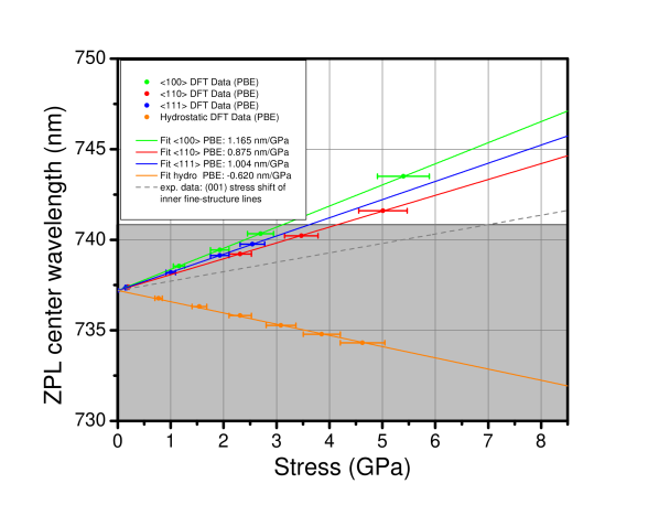
The data points in Figure 6 show the ZPL center wavelength shifts calculated with the method outlined above. For comparison with experimentally determined stress data the strain values of the theoretical calculation were converted into stress assuming a simplified model where diamond is approximated as isotropic linear elastic material. In this case stress is related to strain via Young’s modulus : . This assumption is pragmatic as we do not know the orientation of stress in the nanodiamonds from the Raman measurements but only its modulus. The values of vary considerably among different diamond materials [53] but even nanocrystalline diamond may obtain a large Young’s modulus GPa [54]. As an average value for the nanodiamond size used in our investigations we assume GPa [53]. The calculated data points were extrapolated by linear fit functions to yield stress shift coefficients for the range of stress (up to GPa) found in the nanodiamonds. The grey area covers the wavelength range of experimental ZPL wavelengths measured within group V. The dashed grey line represents stress-shifts of SiV emission lines at low temperatures derived from the only experimentally measured stress shift coefficient for the SiV center under uniaxial stress in direction [55, 56]. The measurements of [55] were performed at 4 K and reveal the shifts of the SiV center fine structure lines: the outer lines of this fine structure shift with about 4 nm/GPa (2.23 THz/GPa, not shown here), whereas the inner lines shift with only 0.52nm/GPa (292 GHz/GPa, denoted as dashed line). The room temperature spectrum, however, is mostly governed by the inner line ”C” of the spectrum [6], i.e. the line with second highest wavelength, corresponding to the optical transition between the lower branch levels of the and doublets as used in the DFT calculations. We find that the calculated uniaxial stress shift coefficients match well the experimentally obtained value (dashed line) and both coincide well with the range of measured red-shifted ZPLs of group V (grey area). We thus interpret the ZPL shifts of group V as originating from level shifts due to uniaxial strain. Furthermore, the calculated ZPL shifts due to hydrostatic pressure coincide well with the range of the blue shifted ZPLs that we observe in group V. The fact that we see only few blue-shifted ZPLs might be due to reason that pure hydrostatic pressure is rarely observed and overlayed by uniaxial stress in the nanodiamonds.
On the other hand, the measured shifts in group H are too broad to be solely explained by strain in the diamond.
A potential explanation for the very inhomogeneous distribution of defect center ZPL center wavelengths could be the association of SiV centers with a further nearby defect, such as a vacancy, or a modified SiV complex such as SiV:H [57].
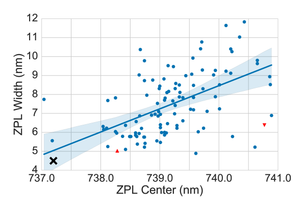
Zooming in to group V, another effect becomes visible (Figure 3(c)):
with increasing ZPL center wavelength, the linewidth becomes broader.
As discussed above, a red-shift of the ZPL is linked to increasing uniaxial strain.
Thus we conclude that the ZPL linewidth, too, is affected by strain in the diamond lattice due to a modified electron-phonon coupling [10]. A similar effect has been previously observed for SiV centers at cryogenic temperatures [6].
To conclude, we are able to explain the distribution of ZPL center wavelengths in group V very consistently with theoretical predictions based on level shifts due to strain in the diamond lattice.
On the other hand, we have to assume that group H is comprised of modified SiV centers, the structure of which is currently unclear.
3.2.2 Sideband
From the literature it is known, that the SiV center in nanodiamond exhibits a large Debye-Waller factor of over [18, 23], which is consistent with our measurements of emitter H1 and emitter V1. Nevertheless, sideband peaks are present in many SiV center photoluminescence emission spectra. The investigated emitters exhibit two different structures of sideband spectra: The spectra in group V exhibit one strong sideband peak (Figure 7), whereas spectra in group H exhibit several weaker sideband peaks.
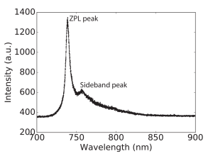
About of the group V photoluminescence spectra with one distinct sideband peak display a shift of the sideband peak from the ZPL between . The range of line shifts for the prominent sideband peak coincides with a well-known feature at , associated with SiV centers [55, 58], but also to a larger number of optically active defects [55]. The occurrence of this sideband feature for a large number of defects and the absence of isotopic variations [36], favors an assignment as non-localized lattice vibration. We furthermore observe that the dominant sideband peak shifts towards smaller distance from the ZPL for increasing ZPL center wavelength, i.e. increasing strain, see Figure 8.
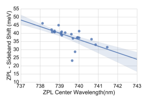
We fit the data with a linear regression and find a slope of meV nm-1.
The low phonon energy of the sideband feature and its shift with strain might arise from a local “softening” of the crystal lattice in the vicinity of a defect [55].
A recent study [59] suggests that the mode (as other broad sideband features) originates from a resonance of . phonons causing the dynamical Jahn-Teller effect in the SiV centers.
As the Jahn-Teller coupling varies with strain it is also expected that the resonance shifts accordingly.
In the spectra of group V, we do not observe a typical SiV center sideband feature at , attributed to a local vibration of the silicon atom [36], frequently much stronger than the sideband peak.
A possible explanation is, that the lattice mode at is so strong that the local vibrational mode at cannot be separated from the tail of the lattice mode.
In group H we observe many spectra which exhibit several peaks within the spectral range of our detection range between .
The challenge arises to unequivocally distinguish between peaks stemming from a phonon sideband and peaks stemming from shifted, less intense SiV center ZPLs.
We see, however, a tendency of peaks to accumulate at shifts of around .
These findings are consistent with sideband shifts reported in [23, 55, 60].
3.3 Photon correlation measurements
The investigated individual SiV centers exhibit count rates of a few thousand to a few counts per second ().
We carried out measurements of the photon statistics and found that about of luminescent nanodiamonds contain single color centers.
Our measurements further reveal that the probability of finding a single emitter does not correlate in any way with the center wavelength or the linewidth of the ZPL.
We found several single SiV centers with an antibunching dip down to about and attribute the residual value to background fluorescence from the diamond host.
For the nanodiamonds used in our investigations an independent background measurement without simultaneously measuring SiV center photoluminescence is infeasible, because the laser spot size is bigger than the nanodiamond.
Therefore, the background is estimated from the sideband of SiV center spectra.
The measured lifetimes of the single SiV centers are in the range of about in accordance with previous research [8, 18, 55].
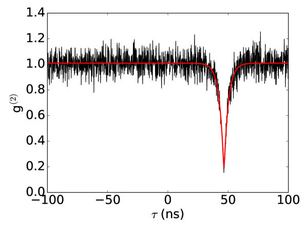
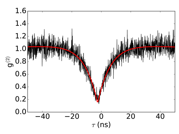
Figure 9 shows the functions of the two emitters introduced in subsection 3.2, emitter H1 and emitter V1.
9(a) shows the photon correlation function of an emitter in group H.
The shift of the dip to originates from a path length difference of the two detection paths in the Hanbury Brown and Twiss setup.
The value of the fit is due to residual background as discussed above.
The excited state lifetime of the emitter was determined to be .
9(b) shows the function of emitter V1 at an excitation power of , which is of the emitter’s saturation power .
The value yields .
The lifetime of the excited state of this emitter is which is the highest excited state lifetime we measured within this work.
Several nanodiamond photoluminescence spectra contain multiple narrow distinct peaks at different wavelengths.
This circumstance is attributed to nanodiamonds containing more than one SiV center, each of which is subject to a different ZPL wavelength shift.
We choose narrow bandpass filters to perform independent measurements of each individual peaks of such a spectrum.
As a result it is possible to measure values below for each of these narrow peaks.
Hence the individual peaks are identified as single emitters with a different ZPL center wavelength.
We do not see a systematic difference regarding the photon autocorrelation functions of group H and group V, both reach similar values.
Also, the timescales of the excited state lifetimes coincide.
3.4 Photostability
As mentioned in the previous section, the single photon count rates observed from the investigated SiV centers varies strongly between a few thousand to a few .
To further investigate the count rate, the luminescence time trajectory of the emitters which exhibit a dip at is evaluated.
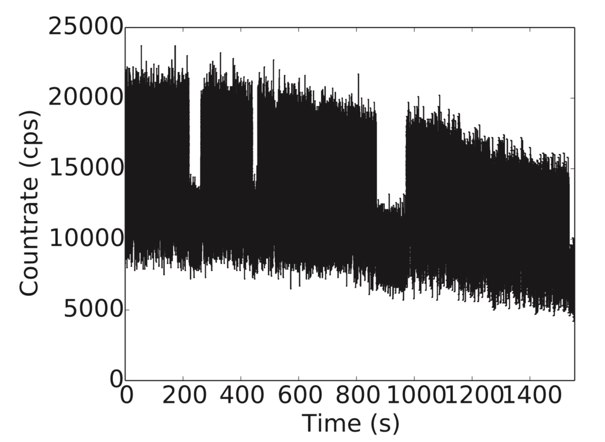
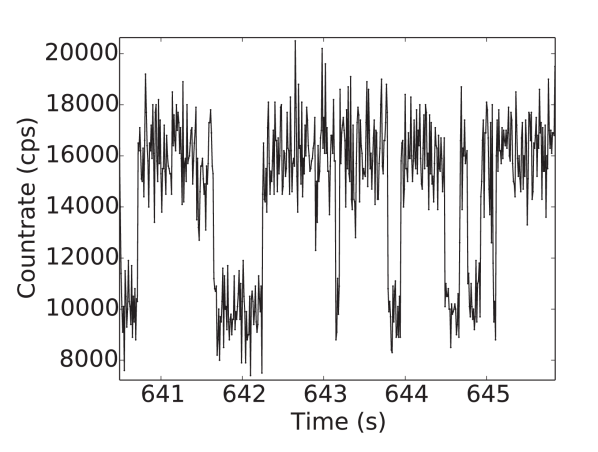
It is found that some of the observed emitters exhibit fluorescence intermittence, also called blinking (Figure 10).
Blinking is attributed to temporal ionization of the color center during optical excitation, forming a
charge state which is optically inactive or emitting outside the detection window [21, 29, 61].
Therefore the emitters change between states of higher and lower emission, i.e. brighter and darker states, called blinking levels.
The photon count time trace of emitter emitter H1 is shown in Figure 10.
In the overview picture (10(a)), a few blinking dips can be seen with time intervals of up to a few minutes.
The fact that the count rate never drops down to the dark count rate lets us assume, that there are at least two SiV centers present, one exhibiting fluorescence intermittence and one exhibiting a stable emission.
When zooming in, shorter time intervals are observable (10(b)).
The time intervals range from a few tens of milliseconds up to a few seconds with a few outliers exhibiting very long time intervals up to a few hundred seconds.
The bright and dark times exhibit different probability distribution functions and with that, different characteristic time constants.
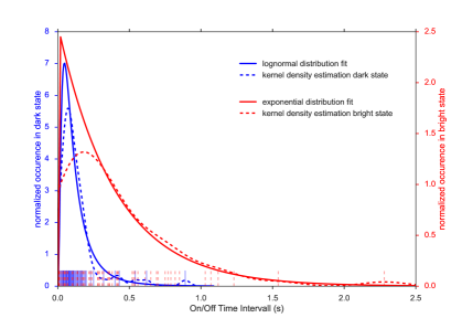
In Figure 11 the time intervals of the emitter are shown as small vertical dashed red lines and solid blue lines for the bright and dark state respectively.
Outliers with very long time intervals are ommited here.
The dashed lines are kernel density estimators of the distribution of the respective time intervals.
This implies that every data point is represented with a Gaussian function and the resulting functions are added up to model the whole data.
The red solid line is an exponential fit of the distribution of time intervals in the bright state.
The high p-value of confirms the goodness of the fit.
The median time interval in the bright state obtained by the exponential fit amounts to .
While other literature on solid state quantum emitters reports an exponential probability distribution for both time intervals in bright and dark states[62, 63], we found a log-normal probability distribution for the time interval in the dark state.
The solid blue line in Figure 11 is a log-normal fit of the distribution of the time intervals in the dark state.
A Kolomogorov-Smirnov test yields a p-value of for the log-normal fit and is by far the best model to describe the data distribution.
For comparison, the p-value of an exponential fit amounts to .
The median time interval in the dark state obtained by the log-normal fit is determined as , therefore being close to the median time interval in the bright state.
Very long time intervals are not shown in the plot for better visualization of the small timescales, however these long time intervals are included in the fit.
The longest measured time interval amounted to and occurred in the dark state.
Measurements of SiV center blinking time intervals in [21] and [29] report time intervals between about , and to , respectively.
These findings are in good agreement with our measurements. We do not identify a correlation between the count rate of a blinking state and its temporal duration.
However, a correlation between the position in the bimodal distribution and blinking is established:
All but one emitters in group H exhibit blinking, where only one of the emitters in group V exhibits blinking (Figure 3).
This dependency suggests that emitters in strained nanodiamonds are more likely to exhibit blinking.
As blinking is typically linked to temporary loss of photo-excited charges we tentatively explain the observed blinking as a manifestation of the local crystal disorder due to dislocations and impurities which act as a trap for the excited electron and therefore switch the emitter to the dark state [62].
The assumption that dislocations and impurities are responsible for blinking emitters is in agreement with our findings reported in 3.1. Regarding the time interval distributions, e.g. research of blinking rhodamine molecules confirmed power law distributed bright state times and log-normal distributed dark state times [64]. Log-normal distributions are typically explained by a Gaussian distribution of activation barriers of the electron transfer to trap states in the surrounding material [65] which hints towards a recapture of the electron via multi-phonon relaxation channels.
4 Conclusion
In conclusion, in this work we report on a strongly inhomogeneous distribution of SiV center spectra in nanodiamonds produced by wet milling from polycrystalline diamond films.
We find that the zero phonon lines of the emission spectra can be grouped into two clusters:
Group H consists of ZPLs exhibiting a narrow linewidth from below up to and a broad distribution of center wavelength between .
Compared to that, group V comprises ZPLs with a broad linewidth between just below and center wavelength ranging from .
Based on ab initio density functional theory calculations we show that both the observed blue-shifts and red-shifts of the ZPLs of group V (as compared to an ideal, unstrained SiV center) are consistently explained by strain in the diamond lattice. Further, we suggest, that group H might be comprised of modified SiV centers, the structure of which is currently
unclear.
The broad distribution of emission wavelengths found here covers all earlier results on spectroscopy of SiV centers but considerably extends the range of known emission wavelengths. It further suggests that some single photon emitters in the nm range, previously identified as Cr-, Ni- or Ni/Si-related (see e.g. [66]), could indeed exist of strained or perturbed SiV centers.
Whereas single photon emission could be demonstrated for SiV centers of both clusters, we show that the two clusters of SiV centers show different spectroscopic features: For the phonon sideband spectra we find in
group V one prominent peak at a shift of , which corresponds to a well-known feature assigned to non-localized lattice vibrations [55, 58].
In group H we see an accumulation of peaks, at around , which are consistent with sideband peaks reported in [23, 30, 55].
Investigating the time trace of the SiV center photoluminescence, we found that predominantly SiV centers with narrowband emission (group H) exhibit fluorescence intermittence with on/off times between several microseconds up to .
Furthermore, we see an exponential distribution of bright time intervals and a log-normal distribution of dark time intervals, consistent with research on single molecules [64].
In summary, whereas SiV centers produced by ion implantation in high quality bulk diamond material show very reproducible spectral properties, SiV centers in nanodiamonds produced by milling techniques or CVD growth feature strongly varying optical spectra. This, on one hand, limits their applicability for quantum information tasks requiring indistinguishable emitters and, on the other hand, demonstrates the need for development of low-strain, nanometer-sized diamond material with low defect density.
References
- [1] Becker J N, Pingault B, Groß D, Gündogan M, Kukharchyk N, Markham M, Edmonds A, Atatüre M, Bushev P and Becher C 2018 Phys. Rev. Lett. 120 053603
- [2] Becker J N and Becher C 2017 Phys. Status Solidi A 214 1700586
- [3] Sukachev D D, Sipahigil A, Nguyen C T, Bhaskar M K, Evans R E, Jelezko F and Lukin M D 2017 Phys. Rev. Lett. 119 223602
- [4] Rogers L J, Jahnke K D, Metsch M H, Sipahigil A, Binder J M, Teraji T, Sumiya H, Isoya J, Lukin M D, Hemmer P and Jelezko F 2014 Phys. Rev. Lett. 113 263602
- [5] Rogers L J, Jahnke K D, Teraji T, Marseglia L, Müller C, Naydenov B, Schauffert H, Kranz C, Isoya J, McGuinness L P and Jelezko F 2014 Nature Commun. 5 4739
- [6] Arend C, Becker J N, Sternschulte H, Steinmüller-Nethl D and Becher C 2016 Phys. Rev. B 94 045203
- [7] Schröder T, Trusheim M E, Walsh M, Li L, Zheng J, Schukraft M, Sipahigil A, Evans R E, Sukachev D D, Nguyen C T, Pacheco J L, Camacho R M, Bielejec E S, Lukin M D and Englund D 2017 Nature Commun. 8 15376
- [8] Sipahigil A, Jahnke K D, Rogers L J, Teraji T, Isoya J, Zibrov A S, Jelezko F and Lukin M D 2014 Phys. Rev. Lett. 113 113602
- [9] Sipahigil A, Evans R E, Sukachev D D, Burek M J, Borregaard J, Bhaskar M K, Nguyen C T, Pacheco J L, Atikian H A, Meuwly C, Camacho R M, Jelezko F, Bielejec E, Park H, Lončar M and Lukin M D 2016 Science 354 847–850
- [10] Jahnke K D, Sipahigil A, Binder J M, Doherty M W, Metsch M, Rogers L J, Manson N B, Lukin M D and Jelezko F 2015 New J. Phys. 17 43011
- [11] Baker M 2010 Nature Methods 7 957–962
- [12] Merson T D, Castelletto S, Aharonovich I, Turbic A, Kilpatrick T J and Turnley A M 2013 Opt. Lett. 38 4170
- [13] Albrecht R, Bommer A, Pauly C, Mücklich F, Schell A W, Engel P, Schröder T, Benson O, Reichel J and Becher C 2014 Appl. Phys. Lett. 105 073113
- [14] Benedikter J, Kaupp H, Hümmer T, Liang Y, Bommer A, Becher C, Krueger A, Smith J M, Hänsch T W and Hunger D 2017 Phys. Rev. Applied 7 024031
- [15] Alaverdyan Y, Vamivakas N, Barnes J, Lebouteiller C, Hare J and Atatüre M 2011 Opt. Exp. 19 18175
- [16] Schietinger S, Barth M, Aichele T and Benson O 2009 Nano Lett. 9 (4) 1694–1698
- [17] Schell A, Kewes G, Schröder T, Wolters J, Aichele T and Benson O 2011 Rev. Scient. Inst. 82 073709
- [18] Neu E, Steinmetz D, Riedrich-Möller J, Gsell S, Fischer M, Schreck M and Becher C 2011 New J. Phys. 13 25012
- [19] Davydov V a, Rakhmanina a V, Lyapin S G, Ilichev I D, Boldyrev K N, Shiryaev a a and Agafonov V N 2014 JETP Letters 99 585–589
- [20] Neu E, Arend C, Gross E, Guldner F, Hepp C, Steinmetz D, Zscherpel E, Ghodbane S, Sternschulte H, Steinmüller-Nethl D, Liang Y, Krueger A, Becher C, Al E, al E, Al E and Al E 2011 Appl. Phys. Lett. 98 243107
- [21] Jantzen U, Kurz A B, Rudnicki D S, Schäfermeier C, Jahnke K D, Andersen U L, Davydov V A, Agafonov V N, Kubanek A, Rogers L J and Jelezko F 2016 New J. Phys. 18 073036
- [22] Tran T T, Kianinia M, Bray K, Kim S, Xu Z Q, Gentle A, Sontheimer B, Bradac C and Aharonovich I 2017 APL Photonics 2 116103
- [23] Neu E, Fischer M, Gsell S, Schreck M and Becher C 2011 Phys. Rev. B 84 205211
- [24] Neu E, Hepp C, Hauschild M, Gsell S, Fischer M, Sternschulte H, Steinmüller-Nethl D, Schreck M and Becher C 2013 New J. Phys. 15 043005
- [25] Grudinkin S A, Feoktistov N A, Baranov M A, Smirnov A N, Davydov V Y and Golubev V G 2016 Nanotechnol. 27 395606
- [26] Williams O A and Nesládek M 2006 Phys. status solidi 203 3375–3386
- [27] Bray K, Sandstrom R, Elbadawi C, Fischer M, Schreck M, Shimoni O, Lobo C, Toth M and Aharonovich I 2016 ACS Applied Materials & Interfaces 8 7590–7594
- [28] Zapol P, Sternberg M, Curtiss L, Frauenheim T and Gruen D 2001 Phys. Rev. B 65 045403
- [29] Neu E, Agio M and Becher C 2012 Opt. Exp. 20 19956–19971
- [30] Zaitsev A 2001 Optical properties of diamond: a data handbook
- [31] Prawer S and Nemanich R J 2004 Phil. Trans. R. Soc. Lond. A 362 2537–2565
- [32] Orwa J O, Nugent K W, Jamieson D N and Prawer S 2000 Phys. Rev. B 62 5461–5472
- [33] Ferrari A C and Robertson J 2004 Phil. Trans. R. Soc. Lond. A 362 2477–2512
- [34] Widmann C, Müller-Sebert W, Lang N and Nebel C 2016 Diamond Rel. Mat. 64 1–7
- [35] Liscia E J D, Álvarez F, Burgos E, Halac E B, Huck H and Reinoso M 2013 Mat. Sci. Appl. 04 191–197
- [36] Dietrich A, Jahnke K D, Binder J M, Teraji T, Isoya J, Rogers L J and Jelezko F 2014 New J. Phys. 16 113019
- [37] Walker J and Walkert J 1979 Rep. Prog. Phys. 42 1606–1659
- [38] Neu E K 2012 Silicon vacancy color centers in chemical vapor deposition diamond : new insights into promising solid state single photon sources Ph.D. thesis
- [39] Deák P, Aradi B, Kaviani M, Frauenheim T and Gali A 2014 Phys. Rev. B 89(7) 075203
- [40] Kaviani M, Deák P, Aradi B, Frauenheim T, Chou J P and Gali A 2014 Nano Lett. 14 4772–4777 pMID: 25054621
- [41] Kresse G and Hafner J 1993 Phys. Rev. B 47(1) 558–561
- [42] Kresse G and Furthmüller J 1996 Computational Materials Science 6 15 – 50
- [43] Kresse G and Furthmüller J 1996 Phys. Rev. B 54(16) 11169–11186
- [44] Kresse G and Joubert D 1999 Phys. Rev. B 59(3) 1758–1775
- [45] Perdew J P, Burke K and Ernzerhof M 1996 Phys. Rev. Lett. 77(18) 3865–3868
- [46] Hepp C, Müller T, Waselowski V, Becker J N, Pingault B, Sternschulte H, Steinmüller-Nethl D, Gali A, Maze J R, Atatüre M and Becher C 2014 Phys. Rev. Lett. 112(3) 036405
- [47] Rogers L J, Jahnke K D, Doherty M W, Dietrich A, McGuinness L P, Müller C, Teraji T, Sumiya H, Isoya J, Manson N B and Jelezko F 2014 Phys. Rev. B 89(23) 235101
- [48] Gali A, Janzén E, Deák P, Kresse G and Kaxiras E 2009 Phys. Rev. Lett. 103(18) 186404
- [49] Heyd J, Scuseria G E and Ernzerhof M 2003 J. Chem. Phys. 118 8207
- [50] Krukau A V, Vydrov O A, Izmaylov A F and Scuseria G E 2006 J. Chem. Phys. 125 224106
- [51] Henkelman G, Uberuaga B P and Jónsson H 2000 J. Chem. Phys. 113 9901–9904
- [52] Thiering G and Gali A 2018 Phys. Rev. X 8(2) 021063
- [53] Hess P 2012 J. Appl. Phys. 111 051101
- [54] Williams O, Kriele A, Hees J, Wolfer M, Müller-Sebert W and Nebel C 2010 Chem. Phys. Lett. 495 84
- [55] Sternschulte H, Thonke K, Sauer R, Münzinger P C and Michler P 1994 Phys. Rev. B 50 14554–14560
- [56] Hepp C 2014 Electronic structure of the silicon vacancy color center in diamond Ph.D. thesis
- [57] Thiering G and Gali A 2015 Phys. Rev. B 92 165203
- [58] Larkins F P and Stoneham A M 1971 J. Phys. C: Solid State Physics 4 143–153
- [59] Londero E, Thiering G, Gali A and Alkauskas A 2016 arXiv 1605.02955
- [60] Zaitsev A M 2000 Phys. Rev. B 61 12909–12922
- [61] Gali A and Maze J R 2013 Phys. Rev. B 88 235205
- [62] Bradac C, Gaebel T, Naidoo N, Sellars M J, Twamley J, Brown L J, Barnard A S, Plakhotnik T, Zvyagin A V and Rabeau J R 2010 Nature Nanotechnol. 5 345–9
- [63] Berhane A M, Bradac C and Aharonovich I 2017 Phys. Rev. B 96 041203
- [64] Wong N Z, Ogata A F and Wustholz K L 2013 J. Phys. Chem. C 117 21075–21085
- [65] Albery W J, Bartlett P N, Wilde C P and Darwent J R 1985 J. Am. Chem. Soc. 107 1854–1858
- [66] Aharonovich I, Castelletto S, Simpson D A, Su C H, Greentree A D and Prawer S 2011 Rep. Prog. Phys. 74 076501