Spin-orbit splitting of the conduction band in HgTe quantum wells: role of different mechanisms
Abstract
Spin-orbit splitting of conduction band in HgTe quantum wells was studied experimentally. In order to recognize the role of different mechanisms, we carried out detailed measurements of the Shubnikov-de Haas oscillations in gated structures with a quantum well widths from to nm over a wide range of electron density. With increasing electron density controlled by the gate voltage, splitting of the maximum of the Fourier spectrum into two components and and the appearance of the low-frequency component was observed. Analysis of these results shows that the components and give the electron densities and in spin-orbit split subbands while the component results from magneto-intersubband oscillations so that . Comparison of these data with results of self-consistent calculations carried out within the framework of four-band kP-model shows that a main contribution to spin-orbit splitting comes from the Bychkov-Rashba effect. Contribution of the interface inversion asymmetry to the splitting of the conduction band turns out to be four-to-five times less than that for the valence band in the same structures.
pacs:
73.40.-c, 73.21.Fg, 73.63.HsI Introduction
The energy spectrum of semiconductors, which contain heavy elements, is determined to a significant degree by the spin-orbit (SO) interaction. In bulk semiconductors, the SO interaction in the crystal field, as a rule, is directly included in the Hamiltonian. Just this interaction determines the splitting of the valence band in semiconductors A3B5, A2B6, etc., and, thus, the energy distance between the bands and for zero quasimomentum value, . The absence of an inversion center in these materials leads to an additional splitting for .
In two-dimensional (2D) systems, other mechanisms of SO interaction become important. The first one is caused by a structure inverse asymmetry resulting from different barrier heights, the asymmetry of doping, the gradient of the composition in the quantum well (QW) in the case when it consists of a multicomponent semiconductor. The second mechanism is the interface inverse asymmetry (IIA), and finally the potential gradient in a direction perpendicular to the 2D plane can play a crucial role. The latter mechanism, known as Bychkov-Rashba (BR) effect, is of particular interest, since it can be controlled in the gated structures.
Experimental studies of the valence band spectrum in HgTe quantum wells [1, 2] show that the valence band is strongly split in the structures with different QW width (); both for close to the critical width nm at which the massless Dirac-like spectrum is realized and for nm, where additional maxima at turn out to lie higher in the energy than the hole states at . The calculations of spectrum with taking into account IIA [1] show reasonable agreement with the experimental results on the splitting of the top of the valence band. Such calculations also predict a large splitting of the conduction band at a low electron density. However, in structures with close to no noticeable splitting was experimentally observed for cm-2. Spin-orbit splitting of the conduction band was observed and studied mainly in wide quantum wells, nm, for relatively high electron density, cm-2, and was interpreted as a result of the BR effect [3, 4, 5, 6]. Thus, the role of various mechanisms for the SO splitting of the conduction band and their dependence on the QW width and the electron density remains unclear yet.
In this paper, in order to determine the role of different mechanisms of SO interaction, we carried out detailed measurements of the Shubnikov-de Haas (SdH) oscillations in structures with the quantum well width from to nm over a wide range of electron density. We observed appearance of three components in the Fourier spectra with the frequencies , , and when the electron density increases with the increasing gate voltage (). An analysis of these results shows that the and components give the electron densities and in the SO split subbands while the component results from magneto-intersubband oscillations and it is equal to . The SO splitting is quantified here as , where , can be experimentally found both as and as . Comparison of these results with the self-consistent calculations carried out within the four-band kP model shows that the main contribution to the SO splitting comes from the BR effect while the IIA contribution is less than percent.
II Experiment
The HgTe quantum wells were realized on the basis of HgTe/CdxHg1-xTe () heterostructure grown by molecular beam epitaxy on GaAs substrate with the (), (), and () surface orientation [7]. The nominal QW widths were nm. The samples were mesa etched into standard Hall bars of mm width with the distance between the potential probes of mm. To change and control the electron densities in the quantum well, the field-effect transistors were fabricated with parylene as an insulator and aluminium as a gate electrode. The measurements were performed at the temperature K in the magnetic field up to T. For each heterostructure, several samples were fabricated and studied. The main parameters are listed in the Table 1.
| number | structure | (nm) | substrate orientation | |
|---|---|---|---|---|
| 1 | 100623 | 18 | (100) | |
| 2 | 091228 | 14 | (211) | |
| 3 | 150224 | 10 | (013) | |
| 4 | 150629 | 8.3 | (013) |
III Results and discussion
The experimental results and their analysis for all the structures are similar, therefore, as an example, let us consideer in more detail the data obtained for the structure 100623 with nm. In Fig. 1(a), we present the dependences of transverse magnetoresistance () on a magnetic field () for different gate voltages. As seen, linearly increases with in low magnetic fields, then the oscillations appear, which are transformed to the quantum Hall effect (QHE) steps in the higher magnetic field.
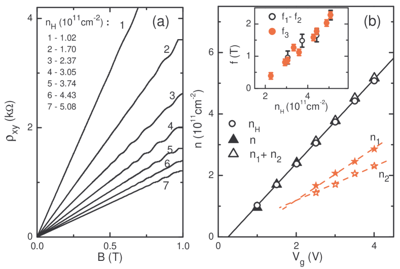
The dependence of the electron density obtained from the Hall effect as plotted in Fig. 1(b) shows that this dependence is linear, , cm-2 with cm-2V-1. This value is in a good agreement with found from the capacitance measurements , where is the capacitance between the 2D gas and the gate electrode, measured for the same structure, is the gated area. The oscillating part of magnetoresistance obtained by extracting the monotonic part , , for some gate voltages and the Fourier spectra of these oscillations found in magnetic field range before onset of the QHE steps are shown in Figs. 2(a) and Figs. 2(b), respectively. These data show that unsplit oscillations with one component in the Fourier spectrum are observed for low electron density cm-2.
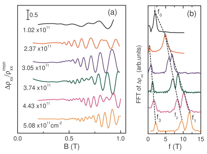
For the higher electron densities the beating of oscillations becomes clearly evident, the component in the Fourier spectrum is split and two maxima, and, arise in the Fourier spectra. The electron densities found from supposing two-fold degeneracy of the Landau levels are shown in Fig. 1(b) by the solid triangles. The electron densities found from and supposing one-fold degeneracy of the Landau levels , are shown by the stars in Fig. 1(b) and the sum of these densities is shown by the open triangles. One can see that and coincide with the Hall densities within experimental accuracy. The above results show that the splitting of the SdH oscillations observed at cm-2 is a consequence of the SO splitting of the spectrum, and and are the densities in the SO split subbands.
The origin of the low-frequency oscillations that give the pick in the Fourier spectra becomes clear from the inset in Fig. 1(b), which demonstrates that is equal to . This denotes that the low-frequency oscillations are a consequence of intersubband transitions, known as magneto-intersubband oscillations (MISO). This conclusion is confirmed also by the temperature dependence of the amplitude of these oscillations, which, as the theory predicts [8, 9, 10, 11], should decrease slowly with the increasing temperature (see Fig. 3). A detailed analysis of MISO is beyond the scope of this paper.
As mentioned above the SO splitting can be characterized by the quantity . Experimentally, it can be found by two ways; as
| (1) |
or as
| (2) |
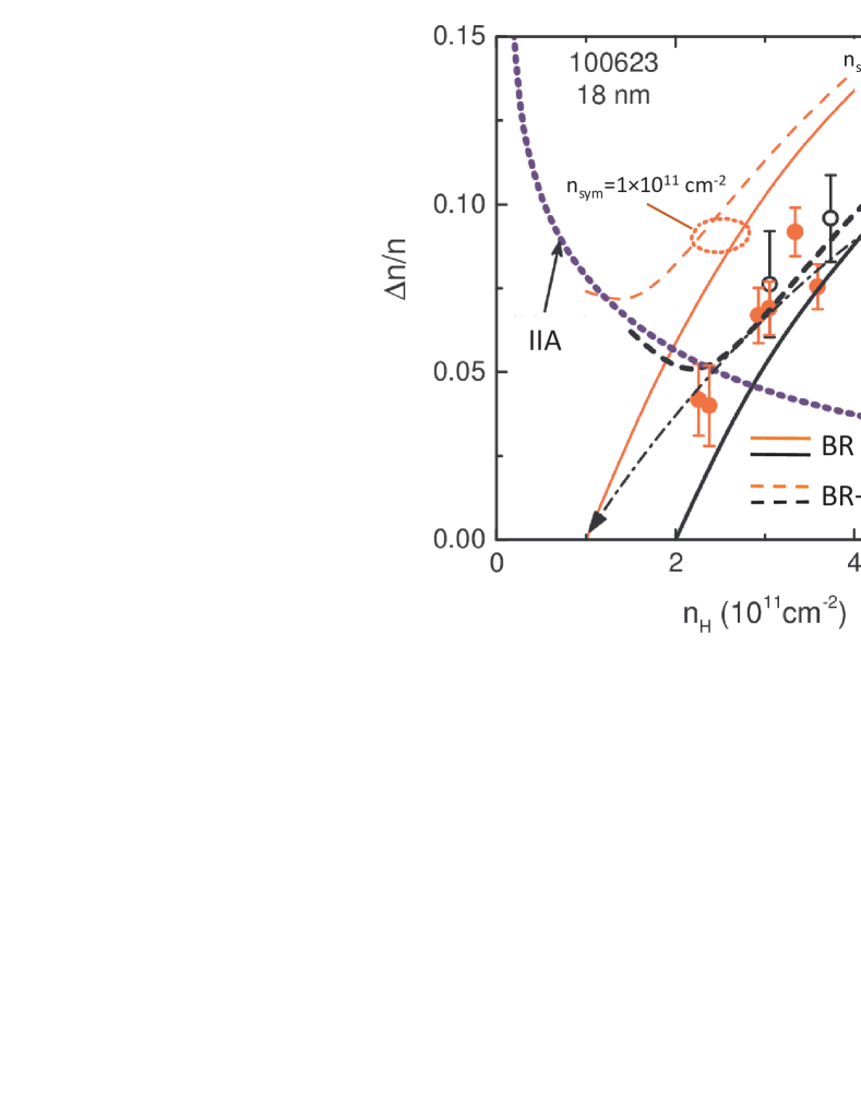
This approach has been used to obtain the SO splitting as a function of the electron density at relatively high electron density, cm-2. The results are presented in Fig. 4. It can be seen that the values of splitting determined with the use of Eq. (1) and Eq. (2) agree well with each other. Therewith, the SO splitting decreases with the decreasing electron density (with the decreasing gate voltage).
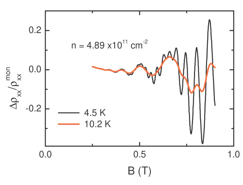
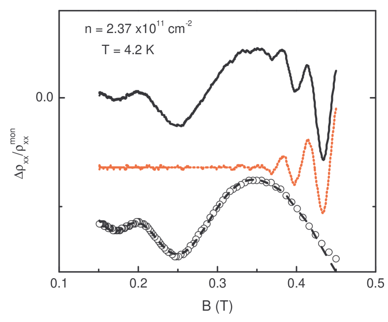
At cm-2, the splitting of the peak ceases to be resolved (see Fig. 2). In this case, can only be determined by analyzing the MISO plot . To extract MISO from the complicated experimental curve (see Fig. 5, the upper line) we have decomposed the experimental oscillations into the low- and high frequency components using the Fourier transformation and the low- and high-pass filtration. The frequency of the low-frequency oscillations (i.e. MISO) was determined from the fit by the Lifshitz-Kosevich-like formula, as demonstrated in Fig. 5.
Now we are in position to compare the experimental results with the theoretical calculations. To do this a self-consistent calculation of spectrum was performed within the framework of the four-band kP method which allows us to take into account both the interface inversion asymmetry and the BR effect (we used the parameters from Ref. [12]) 111The calculations were performed for three QW orientations corresponding to the structure under investigation. The difference in SO splitting does not exceed percent. For such a calculation, it is necessary to specify the electron density () at which the electric potential in the quantum well is symmetric. As the first step, let us determine this value by eye, extrapolating the experimental data to zero value as shown by the dash-dotted line in Fig. 4. Doing so we get cm-2. The results of the calculation without and with taking into account IIA are shown in Fig. 4 by the upper solid and dashed curves, respectively 222We used eV [2]. This value gives a good agreement with the experimental splitting values of the top of the valence band in the structures with , in which the top of the valence band is located at [1]. It can be seen that these dependences lie noticeably higher than the experimental values. The same figure shows the calculation results for the other value, cm-2 (the lower solid and dashed curves in Fig. 4). In this case, as seen, both curves describe the experimental data equally well. For clarity, we present by the doted curve the dependence calculated with taking into account the IIA only. It is apparent that IIA gives a large contribution to at the electron density close to cm-2 and a small contribution at the higher density, where practically all the experimental points lie. We would like to note here that the additive sum of curves, calculated with taking into account only the interface inversion asymmetry or the BR effect separately does not coincide with the curve calculated with taking into account both mechanisms.
Thus, analysis of the results obtained on the structure with the QW width of nm shows that the Bychkov-Rashba effect is the main cause of the SO splitting, while the IIA contribution to SO splitting is small and cannot be determined quantitatively.
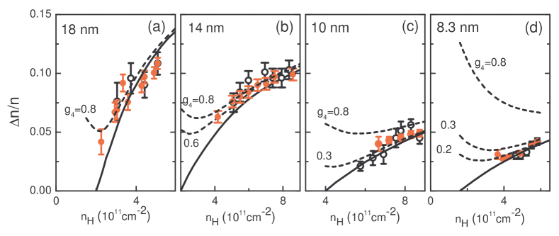
The above measurements and analysis were carried out for all the structures listed in the Table 1. The results are summarized in Fig. 6. It is seen that as the QW width decreases, both the value and the rate of change of decrease significantly, so it is more difficult to determine . Nevertheless, this can be done in the structure with nm. Note that for cm-2, the value can only be determined from low-frequency oscillations, i.e. from MISO. The separation of MISO and determination of was analogous to that described above for the structure with nm (see Fig. 5).
Figure 6 shows as well the results of calculating , similar to those described above, for the structure 100623 with nm. It can be seen that taking into account only the BR mechanism allows us to describe the experimental dependences for all the structures well (see the solid curves in Fig. 6). Satisfactory agreement of the theory with the data can also be obtained with an additional taking into account of IIA (see the dashed curves in Fig. 6). However, we must monotonically reduce the upper value of the parameter with decreasing QW width.
These results show that the contribution of IIA to SO splitting is small in comparison with the BR effect, which makes it impossible to quantify its contribution. Only in the structure 150629 with nm, accounting for IIA gives a somewhat better agreement with the experiment [see Fig. 6(d)]. Therewith, the value corresponding to the best agreement, , turns out to be four times lower than it was required in the analysis of the splitting of the valence band in Ref. [2]. This result seems strange. The matter is that the SO splitting due to IIA is a result of different mixing of the states at the opposite QW interfaces. This mixing is described by the same parameter both for the valence and for conduction band within the framework of the model used. From our point of view, this shows that the usually used theoretical model does not take into account something important.
Let us discuss what approximations were made when analyzing the data. First, the use of Eq. (1) for the determination of means that we neglect the contribution of the Zeeman splitting in comparison with the spin-orbit splitting. Simultaneous accounting for the Zeeman and SO splitting leads to more complicated expression for the magnetic field dependence of the Landau level energies [15] from which it follows that the oscillation frequencies become dependent on the magnetic field because the Zeeman splitting increases linearly with increase while the SO splitting is independent of magnetic field. Our estimations show that neglect of the Zeeman splitting when treating the data at T results in error in determination of less than percent for the our electron density range.
Second, we do not take into account the Dresselhaus contribution to SO splitting in our theoretical considerations. Parameters responsible for this contribution are unknown for HgTe and Hg1-xCdxTe of actual composition. If one uses the parameters for CdTe [15], this contribution is estimated as ten-to-twenty times less than the observed values of .
Finally, we show in Ref. [16] that the experimental electron effective mass is not described within the framework of the kP model in its usual form. We assumed there that this is result of renormalization of the spectrum of the conduction band due to many-body effects. When analyzing SO interaction in the present paper, we also used the kP calculation in its conventional form. We do not know the papers in which the SO interaction is considered taking into account such renormalization. Recall that we were able to estimate the upper value of the IIA contribution from the data for structure with nm. The experimental effective mass obtained for this structure is only percent lower than the calculated value. Therefore we assume that the use of the kP calculations for our case is reasonable.
IV Conclusion
We have presented the results of experimental studies of spin-orbit splitting of the conduction band in HgTe quantum wells. In order to elucidate the role of different mechanisms of SO interaction, we carried out detailed measurements of the SdH oscillations in structures with quantum well widths from to nm over a wide range of electron density. We observed appearance of three components in the Fourier spectra characterized by the frequencies , , and when electron density is increased by the gate voltage. The analysis of these results shows that the and components give the electron densities and in subbands split by SO interaction, while the component results from the magneto-intersubband oscillations and it is determined by the difference between the electron densities in SO split subbands . Treating the Fourier spectra with taking this into account, we have determined the value of the SO splitting over the wide electron density range for all the structures under study. The data obtained were compared with the results of self-consistent calculations carried out within the framework of the four-band -model. It is shown that the main contribution to the SO splitting comes from the Bychkov-Rashba effect while the contribution of the interface inverse asymmetry is less than percent. Thus we have obtained surprising results. In HgTe-QWs, the interface inverse asymmetry is not so important in the SO splitting of the conduction band unlike the valence band, where it plays a crucial role as shown in Refs. [1, 2].
The further experimental and theoretical investigations are needed to solve this puzzle.
Acknowledgements.
We are grateful to I. V. Gornyi and L. E. Golub for useful discussions. The work has been supported in part by the Russian Foundation for Basic Research (Grants No. 16-02-00516 and No. 18-02-00050), by Act 211 Government of the Russian Federation, agreement No. 02.A03.21.0006, by the Ministry of Education and Science of the Russian Federation under Project No. 3.9534.2017/8.9, and by the FASO of Russia (theme “Electron”).References
- Minkov et al. [2016] G. M. Minkov, A. V. Germanenko, O. E. Rut, A. A. Sherstobitov, M. O. Nestoklon, S. A. Dvoretski, and N. N. Mikhailov, Phys. Rev. B 93, 155304 (2016).
- Minkov et al. [2017] G. M. Minkov, V. Y. Aleshkin, O. E. Rut, A. A. Sherstobitov, A. V. Germanenko, S. A. Dvoretski, and N. N. Mikhailov, Phys. Rev. B 96, 035310 (2017).
- M Schultz et al. [1996] M. M Schultz, F. Heinrichs, U. Merkt, T. Colin, T. Skauli, and S. Løvold, Semicond. Sci. Technol 11, 1168 (1996).
- Zhang et al. [2001] X. C. Zhang, A. Pfeuffer-Jeschke, K. Ortner, V. Hock, H. Buhmann, C. R. Becker, and G. Landwehr, Phys. Rev. B 63, 245305 (2001).
- Zhang et al. [2002] X. C. Zhang, A. Pfeuffer-Jeschke, K. Ortner, C. R. Becker, and G. Landwehr, Phys. Rev. B 65, 045324 (2002).
- Gui et al. [2004] Y. S. Gui, C. R. Becker, N. Dai, J. Liu, Z. J. Qiu, E. G. Novik, M. Schäfer, X. Z. Shu, J. H. Chu, H. Buhmann, and L. W. Molenkamp, Phys. Rev. B 70, 115328 (2004).
- Mikhailov et al. [2006] N. N. Mikhailov, R. N. Smirnov, S. A. Dvoretsky, Y. G. Sidorov, V. A. Shvets, E. V. Spesivtsev, and S. V. Rykhlitski, Int. J. Nanotechnology 3, 120 (2006).
- Polyanovsky [1988] V. Polyanovsky, Fiz. Tekh. Poluprovodn. 22, 2230 (1988), [Sov. Phys. Semicond. 22, 1408 (1988)].
- Leadley et al. [1988] D. Leadley, M. Brummell, R. Nicholas, J. Harris, and C. Foxon, Solid-State Electronics 31, 781 (1988).
- Sander et al. [1998] T. H. Sander, S. N. Holmes, J. J. Harris, D. K. Maude, and J. C. Portal, Phys. Rev. B 58, 13856 (1998).
- Rowe et al. [2001] A. C. H. Rowe, J. Nehls, R. A. Stradling, and R. S. Ferguson, Phys. Rev. B 63, 201307 (2001).
- Novik et al. [2005] E. G. Novik, A. Pfeuffer-Jeschke, T. Jungwirth, V. Latussek, C. R. Becker, G. Landwehr, H. Buhmann, and L. W. Molenkamp, Phys. Rev. B 72, 035321 (2005).
- Note [1] The calculations were performed for three QW orientations corresponding to the structure under investigation. The difference in SO splitting does not exceed percent.
- Note [2] We used eV [2]. This value gives a good agreement with the experimental splitting values of the top of the valence band in the structures with , in which the top of the valence band is located at [1].
- Winkler [2003] R. Winkler, Spin-orbit coupling effects in two-dimensional electron and hole systems (Springer, Berlin, 2003) p. 194.
- [16] G. M. Minkov, V. Y. Aleshkin, O. E. Rut, A. A. Sherstobitov, A. V. Germanenko, S. A. Dvoretski, and N. N. Mikhailov, arXiv:1805.09538 [cond-mat.mtrl-sci] .