Transport Measurements of Surface Electrons in 200 nm Deep Helium-Filled Microchannels Above Amorphous Metallic Electrodes
Abstract
We report transport measurements of electrons on helium in a microchannel device where the channels are 200 nm deep and m wide. The channels are fabricated above amorphous metallic Ta40W40Si20, which has surface roughness below 1 nm and minimal variations in work function across the surface due to the absence of polycrystalline grains. We are able to set the electron density in the channels using a ground plane. We estimate a mobility of 300 cm2/Vs and electron densities as high as 2.56. We demonstrate control of the transport using a barrier which enables pinchoff at a central microchannel connecting two reservoirs. The conductance through the central microchannel is measured to be 10 nS for an electron density of 1.58. Our work extends transport measurements of surface electrons to thin helium films in microchannel devices above metallic substrates.
For nearly five decades, the system of electrons floating on the surface of bulk helium has provided a physical platform for studying a wide variety of phenomenaAndrei (1997); Monarkha and Kono (2004). The phase diagram of this system can be further enriched at high electron densities where polaronic states, degenerate electron fluids and superconductivity are predicted to exist Peeters and Platzman (1983); Jiang et al. (1988). This region of the phase diagram is difficult to achieve due to two fundamental barriers. First, bulk helium exhibits a hydrodynamic instability caused by the pressure of the electrons, which limits the maximum achievable electron density above the heliumEtz et al. (1984); Hu and Dahm (1990). Second, because of the strong electron-electron interaction at high densities, the Wigner crystal dominates the phase diagram for temperatures below 1 KGrimes and Adams (1980).
These issues can be mitigated by using thin helium films on a dielectric substrate Etz et al. (1984); Mistura et al. (1997); Jiang et al. (1988). The van der Waals interaction between the helium and the substrate stiffens the film, pushing the hydrodynamic instability to higher electron densities. Further, the presence of the dielectric introduces an image charge which screens the Coulomb interaction and reduces the area of the Wigner crystal in the phase diagram. With the use of substrates that have large dielectric constants, the shielding can be enhanced. A metallic substrate would provide the highest density electron fluid.
A large body of experimental work has pursued these ends. While there is a significant body of work which has examined transport of electrons above insulating substrates, there have been fewer studies of electron transport on metallic substratesEtz et al. (1984); Angrik et al. (2004). The disparity between these two seemingly similar systems arises from the presence of disorder in metallic substrates, which can easily suppress electron transport above the metal and prevent basic transport measurementsKlier et al. (2008).
In this work, we fabricate and measure transport of electrons on a thin film of helium above an amorphous metallic substrate in a microchannel device. In contrast with typical polycrystalline metals, amorphous metals are defined by the lack of translational order on atomic length scales McGlone (2017). As a consequence, the surfaces of thin-film amorphous metals are exceptionally smooth and exhibit homogeneous work function over large areas, making them ideally suited for fabrication of electrodes for electrons on helium.
The amorphous metal used in this work is RF-sputtered Ta40W40Si20 (hereafter TaWSi)McGlone (2017); McGlone et al. (2015, 2017). Fig. 1a shows the topography of a 200 nm thick layer of TaWSi measured using atomic force microscopy in a 5 m 5 m window, with a slice along the indicated line in the middle of the scan shown in Fig. 1b. The RMS roughness is measured to be less than 5 , confirming the smoothness of the surface of the amorphous metal. In addition to these features, we have found that TaWSi is a superconductor with a critical temperature near K. While this property of the metal has no noticeable effect on our measurements, it provides a method of integrating superconducting electronicsYang et al. (2016).

An optical micrograph of the device is shown in Fig. 1c. Electrons are confined to two sets of 3 m microchannels connected by a single central microchannel, similar to the device used by Rees et al. (2012). The microchannels are filled by the capillary action of superfluid helium, which determines the depth of helium in the channels. The channels are defined in a 170 nm layer of TaWSi, referred to as the ground plane. Below the ground plane is a 33 nm layer of insulating Al2O3 yielding 200 nm deep channels. Additional electrodes are defined in metallic layers beneath these channels. A 30 nm thick layer of chromium, referred to as the barrier, underlies the entire device. Above the barrier, the left and right reservoir electrodes are patterned in an additional 50 nm thick layer of TaWSi. Fig. 1d and e show cross-sections of the device along the microchannels above the reservoir electrodes and the central microchannel, respectively. The two reservoirs are separated by a 100 nm gap defined using electron-beam lithography.
The device is placed in a leak-tight copper cell mm above the bulk helium level and cooled to a temperature of 1.7 K. Electrons are emitted onto the sample from a filament, with the ground plane voltage, , set to -0.2 V and with all other electrodes at 0 V. Subsequently, an excitation voltage, is applied to the left reservoir electrode at a frequency of 260 Hz, and the resulting current, , is amplified by a current amplifier (Femto DLPCA-200) connected to the right reservoir electrode and measured using lock-in detection (Stanford Research Systems SR830).
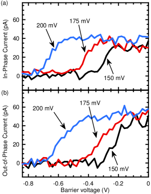
We begin by measuring transport across the device while sweeping the barrier voltage, more negative. Electrical transport through the central microchannel can be controlled by the barrier voltage akin to a field-effect transistor. At low barrier voltages, the central microchannel is open and allows current to flow between the two reservoirs. As the barrier in the central microchannel is increased by sweeping the barrier voltage more negative, the resistance of the central microchannel increases owing to the reduced density of electrons, as reflected by a reduction in the measured current. This behavior continues until the potential at the barrier exceeds the electron potential in the microchannels and the current is turned off completely. In Fig. 2a and b, we show the in-phase and out-of-phase current from the lock-in measurement for three ground plane voltages of mV indicating pinch-off at barrier voltages mV, respectively. These results can be interpreted by considering that more negative ground plane voltages increase the density of electrons in the microchannels, which in turn require larger barrier potentials at the central microchannel to cut off the transport.
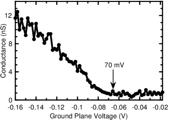
In order to estimate the density of electrons in the microchannels corresponding to the above ground plane voltages, we open the barrier by setting it to 0 V and measure transport between the reservoirs as a function of the ground plane voltage, . The results are shown in Fig. 3. For mV, the channels above the left and right reservoir electrodes are depleted, resulting in no measurable current through the central microchannel. On the other hand, for mV, the conductance is seen to increase up to a saturation value of 12 nS. The voltage sweep shown in Fig. 3 was repeated multiple times, with no appreciable hysteresis, indicating that electrons are readily moved between the channels and the ground plane. In this case, the areal density, , of electrons above the reservoir electrodes can be determined from the relation , where is the dielectric constant of liquid Helium, is the dielectric permittivity of free space, is the electronic charge, and nm is the thickness of the helium level above the reservoir electrodes estimated from the height of the sample above the bulk helium level in our cell. From this expression, we estimate the electron density above the microchannels to be {1.58, 1.97, 2.56} for ground plane voltages of mV, respectively. We note here that non-zero depletion voltage has been observed in other microchannel devicesRees et al. (2012), and is likely due to a combination of work function differences between the different metallic layers as well as thermal offset voltages.
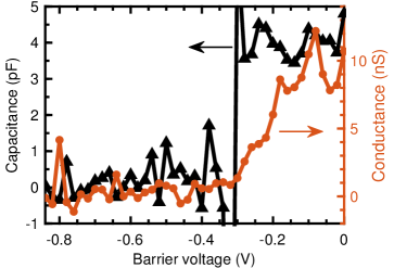
In order to estimate the mobility of the electron transport, we analyze the data for the ground plane voltage set to mV in detail. Assuming that the device can be modeled as a series RC circuit ( due to the central microchannel, and due to coupling to the 2D electron gas in the microchannels above each reservoir electrode), we extract and as a function of barrier voltage. The results of these calculations are shown in Fig. 4. We find that the total capacitance, , remains nearly constant at a value of 4 pF once the barrier is opened, while the conductance increases up to a saturation value of 10 nS. The mobility can then be estimated from the expression where is the number of squares in the central microchannel, is the 2D resistivity and 1.58 is the density of electrons in the microchannels for mV. From this expression, we estimate the mobility of transport in the channels to be 300 cm2/Vs. In addition, from the total area of the microchannels above each reservoir of mm2, we estimate that the channels are half-filled at this density.
We remark here on the assumptions made in the estimate of the mobility. First, we have assumed that the resistance of the transport comes entirely from the central microchannel. This assumption ignores the contribution of the m long microchannels above the reservoirs to the resistance. Additionally, there is a 100 nm gap in the central microchannel that has been used to separate the left and right reservoir electrodes. As an electron moves between the reservoirs, it experiences a resistance due to the discontinuity seen by its image charge at the edges of the gap. Given that the gap width of 100 nm is comparable to the distance of the electron above the reservoir electrodes ( nm), it is likely that the edge contributes to the resistance of the transport. Our estimate of the mobility constitutes a lower bound as a result of these assumptions and further measurements are necessary to separately measure these contributions to the resistance.
The ability to perform measurements with shallow helium has two advantages – first, experiments with microchannel devices that have previously been used where the helium is of order 1 m or thicker can now be extended to shallow helium levels where larger electron densities can be supported. The second benefit is that devices that are typically used in the study of solid-state quantum computation can be realized when gate electrodes can be patterned beneath thin helium films. For example, these gate electrodes can be used to electrostatically define quantum dots for individual electrons on helium, enabling the storage and manipulation of quantum information Dahm (2003); Dykman et al. (2003); Lyon (2006); Schuster et al. (2010).
In conclusion, we have demonstrated transport of electrons on helium in a microchannel device where the channels are only 200 nm deep. The choice of amorphous Ta40W40Si20 as the material for the fabrication of the channels has enabled transport at these depths where the surface roughness and work function variations across the surface are minimized. We have shown the ability to control the transport of electrons across reservoirs using a barrier as well as the ability to set the density of electrons using the ground plane. Future work will investigate shallow devices where higher electron densities can be supported. Additionally, the ability to work with shallow microchannels enables the design of devices where quantum-mechanical effects such as lateral tunneling between quantum dots can be observed.
Acknowledgements.
Devices were fabricated in the Princeton Institute for the Science and Technology of Materials Micro/Nano Fabrication Laboratory and the Princeton University Quantum Device Nanofabrication Laboratory. Work at Princeton was supported by the NSF, in part through Grant No. DMR-1506862, and in part through the Princeton MRSEC (Grant No. DMR-1420541). Sandia National Laboratories is a multimission laboratory managed and operated by National Technology & Engineering Solutions of Sandia, LLC, a wholly owned subsidiary of Honeywell International Inc., for the U.S. Department of Energy’s National Nuclear Security Administration under contract DE-NA0003525. This paper describes objective technical results and analysis. Any subjective views or opinions that might be expressed in the paper do not necessarily represent the views of the U.S. Department of Energy or the United States Government.References
- Andrei (1997) E. Y. Andrei, Two-Dimensional Electron Systems on Helium and other Cryogenic Substrates (Springer Netherlands, 1997).
- Monarkha and Kono (2004) Y. Monarkha and K. Kono, Two-Dimensional Coulomb Liquids and Solids (Springer-Verlag, 2004).
- Peeters and Platzman (1983) F. M. Peeters and P. M. Platzman, Phys. Rev. Lett. 50, 2021 (1983).
- Jiang et al. (1988) H. W. Jiang, M. A. Stan, and A. J. Dahm, Surface Science 196, 1 (1988).
- Etz et al. (1984) H. Etz, W. Gombert, W. Idstein, and P. Leiderer, Phys. Rev. Lett. 53, 2567 (1984).
- Hu and Dahm (1990) X. L. Hu and A. J. Dahm, Phys. Rev. B 42, 2010 (1990).
- Grimes and Adams (1980) C. C. Grimes and G. Adams, Surface Science 98, 1 (1980).
- Mistura et al. (1997) G. Mistura, T. Günzler, S. Neser, and P. Leiderer, Phys. Rev. B 56, 8360 (1997).
- Angrik et al. (2004) J. Angrik, A. Faustein, J. Klier, and P. Leiderer, Journal of Low Temperature Physics 137, 335 (2004).
- Klier et al. (2008) J. Klier, I. Doicescu, P. Leiderer, and V. Shikin, J Low Temp Phys 150, 212 (2008).
- McGlone (2017) J. M. McGlone, Development of Amorphous Metal Thin Films for Thermal Inkjet Printing and Microelectronics, Ph.D. thesis, Oregon State University (2017).
- McGlone et al. (2015) J. M. McGlone, K. R. Olsen, W. F. Stickle, J. E. Abbott, R. A. Pugliese, G. S. Long, D. A. Keszler, and J. F. Wager, Journal of Alloys and Compounds 650, 102 (2015).
- McGlone et al. (2017) J. M. McGlone, K. R. Olsen, W. F. Stickle, J. E. Abbott, R. A. Pugliese, G. S. Long, D. A. Keszler, and J. F. Wager, MRS Communications 7, 715 (2017).
- Yang et al. (2016) G. Yang, A. Fragner, G. Koolstra, L. Ocola, D. Czaplewski, R. Schoelkopf, and D. Schuster, Phys. Rev. X 6, 011031 (2016).
- Rees et al. (2012) D. G. Rees, I. Kuroda, C. A. Marrache-Kikuchi, M. Höfer, P. Leiderer, and K. Kono, J Low Temp Phys 166, 107 (2012).
- Dahm (2003) A. J. Dahm, Low Temperature Physics 29, 489 (2003).
- Dykman et al. (2003) M. I. Dykman, P. M. Platzman, and P. Seddighrad, Phys. Rev. B 67, 155402 (2003).
- Lyon (2006) S. A. Lyon, Phys. Rev. A 74, 052338 (2006).
- Schuster et al. (2010) D. I. Schuster, A. Fragner, M. I. Dykman, S. A. Lyon, and R. J. Schoelkopf, Phys. Rev. Lett. 105, 040503 (2010).