Current splitting and valley polarization in elastically deformed graphene
Abstract
Elastic deformations of graphene can significantly change the flow paths and valley polarization of the electric currents. We investigate these phenomena in graphene nanoribbons with localized out-of-plane deformations by means of tight-binding transport calculations. Such deformations can split the current into two beams of almost completely valley polarized electrons and give rise to a valley voltage. These properties are observed for a fairly wide set of experimentally accessible parameters. We propose a valleytronic nanodevice in which a high polarization of the electrons comes along with a high transmission making the device very efficient. In order to gain a better understanding of these effects, we also treat the system in the continuum limit in which the electronic excitations can be described by the Dirac equation coupled to curvature and a pseudo-magnetic field. Semiclassical trajectories offer then an additional insight into the balance of forces acting on the electrons and provide a convenient tool for predicting the behavior of the current flow paths. The proposed device can also be used for a sensitive measurement of graphene deformations.
I Introduction
One of the remarkable features of graphene and some other 2D materials is the fact that the electrons occupy the valleys around two inequivalent Dirac points in momentum space. This additional valley spin degree of freedom can be used for a new type of electronics, called valleytronics Schaibley et al. (2016). Its key element is an efficient valley polarizer which can separate in space the electrons from the two different valleys. Due to the high interest in this field, several proposals have been already suggested: a graphene valley polarizer can be constructed by using gated constrictions Rycerz et al. (2007); Jones et al. (2017), the trigonal warping of the Dirac cones Garcia-Pomar et al. (2008); Yang et al. (2017), a line defect Gunlycke and White (2011); Ingaramo and Torres (2016), electrostatic potentials in bilayer graphene da Costa et al. (2015), or artificial electron masses with Grujić et al. (2014) or without da Costa et al. (2017) spin-orbit coupling.
Recently, it has been investigated how mechanical deformations affect the electronic properties of graphene, see Vozmediano et al. (2010); Amorim et al. (2016); Naumis et al. (2017) for an overview. It has been shown that a valley polarizer can be constructed by using strained graphene in combination with electrostatic gates Jiang et al. (2013) or magnetic barriers Fujita et al. (2010); Yesilyurt et al. (2016). Moreover, strain alone can lead to valley polarization of the electrons. The required strain patterns are generated, for example, by out-of-plane folds Carrillo-Bastos et al. (2016), bumps Settnes et al. (2016); Milovanović and Peeters (2016) or in-plane wavelike deformations Cavalcante et al. (2016). Some of these deformations have been realized experimentally: bumps Lee et al. (2008); Wong et al. (2010); Shin et al. (2016); Smith et al. (2016) and folds Huang et al. (2011) have been produced in suspended graphene, a bump-like deformation pattern has been engineered recently Nemes-Incze et al. (2017); Georgi et al. (2017) in graphene on a substrate.
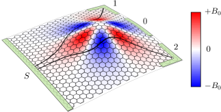
The essential idea of those approaches is to use the pseudo-magnetic field which is produced by the strain. The pseudo-magnetic field for a bump-like deformation is sketched in Fig. 1 by the red and blue color shading. It is oriented perpendicular to the graphene sheet and acts with opposite signs on the two valleys. This valley dependency can be used to separate spatially the electrons from the different valleys. The curved black trajectories in Fig. 1 indicate the deflection of the electrons injected at the source contact in different valleys . The valley polarized electrons can then be extracted at the contacts and .
The general idea to construct an all-strain based valley polarizer has been presented recently in Settnes et al. (2016); Milovanović and Peeters (2016). Here, we extend and significantly improve the previous work. We suggest a new device in which almost complete valley polarization of the electrons comes along with a high transmission (conductance) making our device very efficient. This is achieved because we do not filter out from the injected electrons a small part of valley polarized electrons but we split up all the current into two valley-polarized beams. In contrast to studies of quasi-infinite systems Chaves et al. (2010); Settnes et al. (2016), we attach realistic contacts to the edges of the device in order to quantify the current flow in the system and assess its efficiency. In this way, we obtain a highly efficient valley polarizing device working in a wide range of experimentally accessible parameters.
In our previous work we have developed a geometric language, based on the continuous elasticity theory, for describing current flow paths in deformed graphene Stegmann and Szpak (2016). That approach makes use of the Dirac equation coupled to effective curvature and pseudo-magnetic field. Semiclassical trajectories provide an efficient method to estimate the current flow paths and will also be used to gain additional insight into the system.
II Device and its modeling
We consider a graphene nanoribbon of size . The nanoribbon is described by the tight-binding Hamiltonian
| (1) |
where indicate the atomic states localized on the carbon atoms at positions on sublattices A or B, respectively. The sum runs over nearest neighboring atoms. In homogenous graphene these atoms are separated by a distance of and coupled with the energy
The nanoribbon is deformed elastically by lifting the carbon atoms according to the height function
| (2) |
The center of the deformation is defined by . Its height and width are controlled by the parameters and , respectively. Experimentally, such deformations can be generated by substrate engineering and the tip of atomic force microscope Lee et al. (2008); Wong et al. (2010); Nemes-Incze et al. (2017) or gas pressurized membranes Settnes et al. (2015); Milovanović et al. (2017); Shin et al. (2016); Smith et al. (2016). The modification of the coupling matrix elements is in good approximation described by
| (3) |
where and Pereira et al. (2009); Ribeiro et al. (2009); Carrillo-Bastos et al. (2016).
II.1 The effective Dirac equation in curved space
At low energies, where the electron wavelength is much larger than the lattice constant, and for small deformations the discrete tight-binding Hamiltonian (1) can be approximated by the continuous Dirac Hamiltonian111The spin-connection term, which guarantees hermiticity of the Hamiltonian, can be neglected as a higher order correction. The Dirac equation naturally couples to the curved geometry via a local frame field de Juan et al. (2012); Stegmann and Szpak (2016); de Juan et al. (2013); Oliva-Leyva and Naumis (2015). In Stegmann and Szpak (2016), we demonstrated that the waves propagate along geodesics and therefore, the effective geometry can be assumed to be Riemannian with the metric tensor obtained from the frame. However, for strong deformations the effective current paths may deviate from geodesics and require an extended geometric language, including for example the torsion Zubkov and Volovik (2013); Volovik and Zubkov (2015).
| (4) |
describing relativistic massless fermions in curved space de Juan et al. (2012, 2013); Oliva-Leyva and Naumis (2015); Stegmann and Szpak (2016). Here, is the Fermi velocity of the excited electrons and () are the Pauli matrices. The local frame vectors are determined by the effective strain tensor , which transforms the local frame
| (5) |
Hence, the effective geometry for the electronic excitations is only magnified by the scalar factor but is otherwise identical to the real geometry of the deformed nanoribbon. is a vector potential given by Castro Neto et al. (2009); Vozmediano et al. (2010)
| (6) |
where are two Dirac points of pristine graphene. The curl of this vector potential gives rise to an effective pseudo-magnetic field
| (7) |
which is perpendicular to the graphene plane. In contrast to a true magnetic field, the pseudo-magnetic field acts with the opposite sign in the two different valleys and hence, the time-reversal symmetry of the system is preserved. The change of sign of the pseudo-magnetic field will be used to separate spatially the electrons from the two different valleys, see Fig. 1. The finite curvature expressed by the local frame also affects significantly the transport Stegmann and Szpak (2016). However, it acts equivalently on the two valleys and hence has no effect on the valley polarization.
II.2 Current flow lines in the geometric optics approximation
At low energies and for large-scale deformations, which fulfill the hierarchy
the continuum and geometric optics approximations can be applied to the tight-binding Hamiltonian (1). In our previous work Stegmann and Szpak (2016), we have shown that in that case the current flow in deformed graphene can be predicted by trajectories of relativistic massless fermions which move in a curved space in the presence of a pseudo-magnetic field
| (8) |
where is the “velocity” and the right-hand side terms describe geometric and magnetic forces, respectively ( are Christoffel symbols and is the Levi–Civita symbol).
The calculation of these trajectories is computationally much less demanding than the quantitative quantum approach described in Section II.3 and independent from the system size. Therefore, it provides a useful tool to estimate the current flow in deformed graphene nanostructures, as shown in Fig. 1.
II.3 The nonequilibrium Green’s function method for the current flow
The current flow in graphene nanoribbons is studied quantitatively by means of the nonequilibrium Green’s function (NEGF) method. This quantum method is based on the tight-binding Hamiltonian (1) with hopping parameters (3) modified due to the deformation and a model for the contacts at which the electrons are injected and detected. It does not rely on the Dirac approximation of Section II.1 nor on the geometric optics approximation of Section II.2 and hence, allows us to verify their validity. As the NEGF method is discussed in detail in various textbooks, see e.g. Datta (1997, 2005), we summarize here only briefly the essential formulas.
The Green’s function of the system is given by
| (9) |
where is the single-particle energy of the injected electrons and is the tight-binding Hamiltonian (1). The self-energies describe the effect of the contacts attached to the nanoribbon, see the green bars in Fig. 1.
The electrons are injected at the left ribbon edge as plane waves propagating to the right with momentum . This injection is modeled by the inscattering function
| (10) |
where the sum runs over all carbon atoms in contact with the source. The are the eigenstates of the Dirac Hamiltonian (4) (without any deformation)
| (11) |
where and . The are the amplitudes of the excitations around the two valleys and are used to control the valley polarization of the injected current. The function
| (12) |
gives the injected current beam a Gaussian profile. The parameter , which controls the width of the Gaussian beam, is chosen in such a way that the beam shows minimal diffraction Stegmann and Szpak (2016). Note that using the eigenstates of flat graphene is justified, because has nonzero matrix elements only at the left ribbon edge, where the source contact is located and the deformation vanishes. We assume that the injection of the electrons does not affect their propagation in the graphene nanoribbon and hence, we take .
Three contacts are attached at the right ribbon edge, where the electrons are absorbed and the current flow can be measured, see Fig. 1. For these contacts we use the wide-band model with
| (13) |
where the sum runs over the atoms that are connected to the contact . Moreover, in order to suppress boundary effects, we attach a virtual wide-band contact to those edge atoms which are not connected to a real contact.
The local current flowing between the carbon atoms is calculated by
| (14) |
where
| (15) |
The transmission (or conductance) between the source and one of the three contacts at the right edge (), is given by
| (16) |
The transmission depends not only on the properties of the nanoribbon but also on the size and the model of the contacts attached to it. For a better comparison, we normalize in the following the transmission with respect to the total transmission in a flat nanoribbon.
II.4 Measurement of the valley polarization
The valley polarization of a state can be measured by its projection onto the graphene lattice eigenstates222Here, we chose the eigenstates of the lattice Hamiltonian (1). Projecting onto the eigenstates of the Dirac Hamiltonian (4) gives qualitatively identical results.
| (17) |
where
| (18) |
and is the vector that connects the atoms in sublattice A with the atoms in sublattice B. This projection represents the occupied states in space and hence allows us to determine the valley polarization. Within the NEGF formalism, it can be transformed to
| (19) |
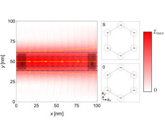
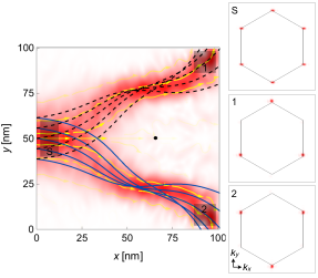
where the projection can be calculated over a finite region of the system, see for example the gray-shaded regions in Fig. 2. The spectral density is integrated in hexagonal regions around the valleys ,
| (20) |
see for example the small hexagons in Fig. 2 (right). The valley polarization is then given by
| (21) |
For the electrons are localized exclusively at the valleys and hence, are completely valley polarized. However, this relative measure can be misleading because it is independent of the current density and hence does not assess how much polarized current is flowing in the system. Our aim is to propose an efficient device, where a high valley polarization of the electrons comes along with a high transmission of the injected current. Hence, we assess the efficiency of our device by multiplying the valley polarization with the corresponding (normalized) transmission,
| (22) |
III Results
III.1 Current flow in flat and deformed graphene nanoribbons
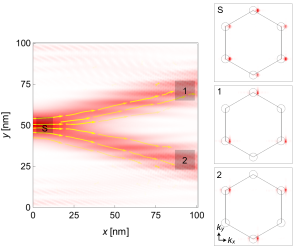
The current flow in a flat graphene nanoribbon without any deformation is shown in Fig. 2. Electrons with energy are injected at the left ribbon edge. The current flows straight along the system indicating ballistic electron transport. Such current paths in graphene nanoribbons have been observed experimentally very recently Tetienne et al. (2017). The projection shows occupied states in all six valleys.333Only two of these valleys are inequivalent, but for clarity we prefer to draw all six of them. The numerical exact agreement of the projections in equivalent valleys provides also a consistency check of our computer code. It confirms that the current is injected unpolarized and remains unpolarized after traversing the system.
The nanoribbon is then deformed in the way described by (2) with width , height and center . This deformation induces a strain of max , which corresponds to changes of the coupling matrix elements by max . Note that we assume that the height and width of the deformation are proportional, which seems to be natural for a deformation caused by the tip of a microscope. It can be observed that due to the interaction with the curvature and the pseudo-magnetic field the current is bent around the deformation, see Fig. 3. The calculation of in the gray-shaded regions indicates clearly that almost all electrons in the upper beam occupy the valley while nearly all electrons in the lower beam are in the valley. This follows from the fact that the pseudo-magnetic field, sketched in Fig. 1, acts with opposite signs on the electrons in different valleys and hence, separates them spatially. Moreover, its interpolating form has the ability to focus the electron beams. The different valley polarizations of the two beams give rise to a finite valley voltage Settnes et al. (2017) between the contacts 1 and 2 (the real voltage is zero as the total currents in both beams are equal).
The current flow lines in the geometric optics approximation, which are indicated by the solid black curves in Fig. 2 and Fig. 3, agree qualitatively with the current obtained by the NEGF method. Hence, the current flow lines can be used for a fast estimation of the local current flow, although they do not provide quantitative information on the current density.
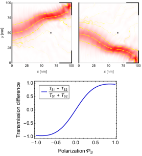
In Fig. 4 (top), valley polarized currents are injected at the left ribbon edge. The current flow paths confirm that the effect of the deformation depends strongly on the valley spin, because electrons at the valley are bent upwards while electrons at the valley are bent downwards. Additionally, we calculate the transmission and between the source at the left and the contacts at the right (see the thick black bars at the edges of Fig. 4 (top)). Their (relative) difference is depicted in Fig. 4 (bottom) and demonstrates that the proposed setup can be used to measure the valley polarization by means of the current detected at the contacts 1 and 2.
III.2 Valley polarization as a function of deformation
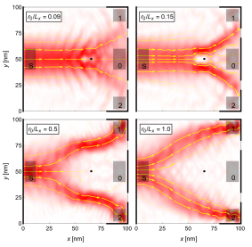
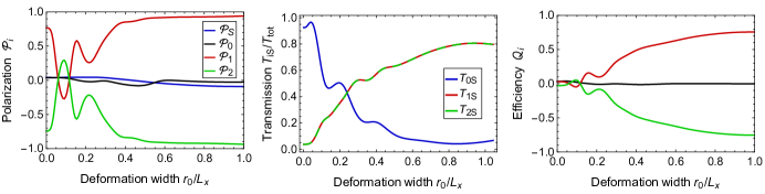
In the following, we study in more detail how the valley polarization is affected by deformations described by (2). We consider the variable width and the height , which grows proportionally to the width. The deformation is centered at . The current flow patterns for various deformations are depicted in Fig. 5 and confirm the expectation that the current deflection increases with the deformation strength. Additionally, we calculate the valley polarization in the gray shaded regions and the transmission between the source at the left and the three contacts at the right (see the thick black bars at the edges of Fig. 5). This allows us to calculate the device efficiency . These quantities are shown as a function of the deformation size in Fig. 6. Note that for symmetry reasons .
In the regions S and 0 the electrons are unpolarized and their polarization is independent of the deformation. In the regions 1 and 2 highly polarized electrons are obtained for but, surprisingly, also in an almost flat system. This behavior can be explained by the fact that the polarization is a relative measure and does not assess how many electrons take part in the flow. In fact, Fig. 2 confirms that in a flat nanoribbon only very few electrons are transfered to the right corners. Their polarization may stem from the trigonal warping of the Dirac cones, see Section III.3 for the discussion. Moreover, for we can observe that the sign of the polarization in the regions 1 and 2 is inverted. This behavior may originate from reflections at the ribbon edges as the deformation is not sufficiently strong to deflect a substantial part of the current, see Fig. 5.
Fig. 6 (middle) shows that the transmissions and increase with the deformation while decreases. This quantifies our observation from Fig. 5 that the deflection of the injected current grows with the increasing deformation. Note that for symmetry reasons . The efficiency of the device, shown in Fig. 6 (right), also increases with the deformation size. It can be observed that for a highly efficient device is obtained where almost all of the injected electrons are split up into two fully polarized electron beams (see also the current flow paths in Fig. 5). The deformation needs to be rather wide in order to catch a significant part of the injected current by the first lobe of the pseudo-magnetic field (see the red lobe closest to the source in Fig. 1) and to split it into two valley polarized beams. Moreover, the functional dependence between the transmission and the deformation size in Fig. 6 (middle) can also be used to determine the deformation of the system from a transport measurement.
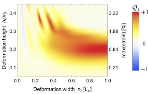
Next, we vary both, the width and height of the deformation independently while keeping its center fixed at . The efficiency at the contact 1 is shown in Fig. 7. Highly efficient valley polarization of the electrons is observed for wide deformations with a height , which corresponds to a maximal strain of . Hence, in the suggested device it is favorable that the pseudo-magnetic field extends over a significant part of the system in order to collect a large part of the injected current. Note that the efficiencies satisfy .
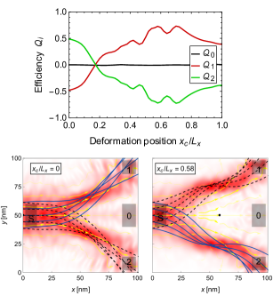
Finally, we vary the position of the deformation in the system while keeping its width and height fixed. The device efficiency , shown in Fig. 8 (left), approaches its maximum when the deformation is placed slightly behind the ribbon center, i.e. at . Surprisingly, we observe that for a deformation, which is centered at the left ribbon edge (), the sign of the efficiency and hence, the sign of the polarization gets reversed. This effect can be explained by the fact that the electrons are injected in the center of the pseudo-magnetic field which acts differently there, see Fig. 1. The classical trajectories in Fig. 8 (right) clearly indicate that the electrons in the two valleys (solid black and blue curves) are deflected differently. However, injecting electrons precisely in the center of a deformation may be experimentally challenging.
III.3 Valley polarization by the trigonal warping of the Dirac cones
As a side remark, we comment that another way to generate a valley polarized current might be to inject electrons at high energy into a flat graphene nanoribbon. In Fig. 9 (left), the electrons that are injected with energy are split into two valley polarized beams. The splitting of the electron beam as well as the valley polarization are due to the trigonal warping of the Dirac cones. This means that at high energies the Fermi surface in graphene is no longer round but becomes triangular, which sends the electrons from the two valleys in two different directions. Details on the graphene valley polarizer based on the trigonal warping of the Dirac cones at high energies can be found in Refs. Garcia-Pomar et al. (2008); Yang et al. (2017). Here, Fig. 9 (right) provides also a consistency check of our calculations because the occupied states are shifted by (small circles) in perfect agreement with the injection energy and the dispersion relation.
IV Conclusions
We studied theoretically the current flow in graphene nanoribbons with smooth out-of-plane deformations (Fig. 1) by means of a tight-binding model and the NEGF method. Already for moderate strains, up to , we observed a complete directional splitting of valley currents (Fig. 3) and a full valley polarization of the separated beams (Fig. 3, 4). The different polarizations of the two beams give rise to a finite valley voltage. We studied the influence of the deformation’s strength (Fig. 5), shape (Fig. 7) and position (Fig. 8) on the current splitting efficiency by measuring the transmission between four contacts (Fig. 6).
To complete the understanding, we established a connection between the current flow paths and classical trajectories of particles moving in curved space in presence of a magnetic field. We derived the latter picture in an earlier work from the effective Dirac equation in deformed graphene Stegmann and Szpak (2016).
These model calculations demonstrate the feasibility of the proposal of a deformation sensor nanodevice. The small size of the system () is only a consequence of our numerical limitations and we expect the phenomena to persist at larger scales as long as the transport stays ballistic. At larger scales () and lower energies () the semiclassical approximation is expected to give even better current flow predictions.
An interesting open topic is the exact form of the bump created in experiments (strain due to lattice mismatch with the substrate, microscope tip, or air pressured membrane) and the spatial distribution of the carbon atoms obtained by taking into account various binding and relaxation mechanisms. Another element of the system, which can be developed further, is the model of the contacts. We plan to quantify the coherence of injected electrons via graphene or hetero-metallic leads and study their influence on polarization efficiency in the transport.
Acknowledgements.
TS acknowledges financial support from CONACYT Proyecto Fronteras 952 and from the UNAM-PAPIIT research grant IA101618. NS acknowledges the support by the “Deutsche Forschungsgemeinschaft” (DFG) through project B7 of the Collaborative Research Centre (SFB) 1242. TS thanks Reyes Garcia for computer technical support. We thank Thomas H. Seligman for useful discussions.References
- Schaibley et al. (2016) J. R. Schaibley, H. Yu, G. Clark, P. Rivera, J. S. Ross, K. L. Seyler, W. Yao, and X. Xu, Nature Rev. Mat. 1, 16055 (2016).
- Rycerz et al. (2007) A. Rycerz, J. Tworzydło, and C. W. J. Beenakker, Nat. Phys. 3, 172 (2007).
- Jones et al. (2017) G. W. Jones, D. A. Bahamon, A. H. C. Neto, and V. M. Pereira, Nano Lett. 17, 5304 (2017).
- Garcia-Pomar et al. (2008) J. L. Garcia-Pomar, A. Cortijo, and M. Nieto-Vesperinas, Phys. Rev. Lett. 100, 236801 (2008).
- Yang et al. (2017) M. Yang, W.-L. Zhang, H. Liu, and Y.-K. Bai, Physica E 88, 182 (2017).
- Gunlycke and White (2011) D. Gunlycke and C. T. White, Phys. Rev. Lett. 106, 136806 (2011).
- Ingaramo and Torres (2016) L. H. Ingaramo and L. E. F. F. Torres, J. Phys.: Condens. Matter 28, 485302 (2016).
- da Costa et al. (2015) D. R. da Costa, A. Chaves, S. H. R. Sena, G. A. Farias, and F. M. Peeters, Phys. Rev. B 92, 045417 (2015).
- Grujić et al. (2014) M. M. Grujić, M. . Tadić, and F. M. Peeters, Phys. Rev. Lett. 113, 046601 (2014).
- da Costa et al. (2017) D. R. da Costa, A. Chaves, G. A. Farias, and F. M. Peeters, J. Phys.: Condens. Matter 29, 215502 (2017).
- Vozmediano et al. (2010) M. Vozmediano, M. Katsnelson, and F. Guinea, Phys. Rep. 496, 109 (2010).
- Amorim et al. (2016) B. Amorim, A. Cortijo, F. de Juan, A. Grushin, F. Guinea, A. Gutiérrez-Rubio, H. Ochoa, V. Parente, R. Roldán, P. San-Jose, et al., Phys. Rep. 617, 1 (2016).
- Naumis et al. (2017) G. G. Naumis, S. Barraza-Lopez, M. Oliva-Leyva, and H. Terrones, Rep. Prog. Phys. 80, 096501 (2017).
- Jiang et al. (2013) Y. Jiang, T. Low, K. Chang, M. I. Katsnelson, and F. Guinea, Phys. Rev. Lett. 110, 046601 (2013).
- Fujita et al. (2010) T. Fujita, M. B. A. Jalil, and S. G. Tan, Appl. Phys. Lett. 97, 043508 (2010).
- Yesilyurt et al. (2016) C. Yesilyurt, S. G. Tan, G. Liang, and M. B. A. Jalil, AIP Advances 6, 056303 (2016).
- Carrillo-Bastos et al. (2016) R. Carrillo-Bastos, C. León, D. Faria, A. Latgé, E. Y. Andrei, and N. Sandler, Phys. Rev. B 94, 125422 (2016).
- Settnes et al. (2016) M. Settnes, S. R. Power, M. Brandbyge, and A.-P. Jauho, Phys. Rev. Lett. 117, 276801 (2016).
- Milovanović and Peeters (2016) S. P. Milovanović and F. M. Peeters, Appl. Phys. Lett. 109, 203108 (2016).
- Cavalcante et al. (2016) L. S. Cavalcante, A. Chaves, D. R. da Costa, G. A. Farias, and F. M. Peeters, Phys. Rev. B 94, 075432 (2016).
- Lee et al. (2008) C. Lee, X. Wei, J. W. Kysar, and J. Hone, Science 321, 385 (2008).
- Wong et al. (2010) C.-L. Wong, M. Annamalai, Z.-Q. Wang, and M. Palaniapan, J. Micromech. Microeng. 20, 115029 (2010).
- Shin et al. (2016) Y. Shin, M. Lozada-Hidalgo, J. L. Sambricio, I. V. Grigorieva, A. K. Geim, and C. Casiraghi, Appl. Phys. Lett. 108, 221907 (2016).
- Smith et al. (2016) A. D. Smith, F. Niklaus, A. Paussa, S. Schröder, A. C. Fischer, M. Sterner, S. Wagner, S. Vaziri, F. Forsberg, D. Esseni, et al., ACS Nano 10, 9879 (2016).
- Huang et al. (2011) M. Huang, T. A. Pascal, H. Kim, W. A. Goddard, and J. R. Greer, Nano Lett. 11, 1241 (2011).
- Nemes-Incze et al. (2017) P. Nemes-Incze, G. Kukucska, J. Koltai, J. Kürti, C. Hwang, L. Tapasztó, and L. P. Biró, Sci. Rep. 7, 3035 (2017).
- Georgi et al. (2017) A. Georgi, P. Nemes-Incze, R. Carrillo-Bastos, D. Faria, S. V. Kusminskiy, D. Zhai, M. Schneider, D. Subramaniam, T. Mashoff, N. M. Freitag, et al., Nano Lett. 17, 2240 (2017).
- Chaves et al. (2010) A. Chaves, L. Covaci, K. Y. Rakhimov, G. A. Farias, and F. M. Peeters, Phys. Rev. B 82, 205430 (2010).
- Stegmann and Szpak (2016) T. Stegmann and N. Szpak, New J. Phys. 18, 053016 (2016).
- Settnes et al. (2015) M. Settnes, S. R. Power, J. Lin, D. H. Petersen, and A.-P. Jauho, J. Phys. Conf. Ser. 647, 012022 (2015).
- Milovanović et al. (2017) S. P. Milovanović, M. . Tadić, and F. M. Peeters, Appl. Phys. Lett. 111, 043101 (2017).
- Pereira et al. (2009) V. M. Pereira, A. H. C. Neto, and N. M. R. Peres, Phys. Rev. B 80, 045401 (2009).
- Ribeiro et al. (2009) R. M. Ribeiro, V. M. Pereira, N. M. R. Peres, P. R. Briddon, and A. H. C. Neto, New J. Phys. 11, 115002 (2009).
- de Juan et al. (2012) F. de Juan, M. Sturla, and M. A. H. Vozmediano, Phys. Rev. Lett. 108, 227205 (2012).
- de Juan et al. (2013) F. de Juan, J. L. Mañes, and M. A. H. Vozmediano, Phys. Rev. B 87, 165131 (2013).
- Oliva-Leyva and Naumis (2015) M. Oliva-Leyva and G. G. Naumis, Phys. Lett. A 379, 2645 (2015).
- Zubkov and Volovik (2013) M. A. Zubkov and G. E. Volovik, in Talk presented at the International Moscow Phenomenology Workshop (2013), URL https://arxiv.org/abs/1308.2249.
- Volovik and Zubkov (2015) G. Volovik and M. Zubkov, Annals of Physics 356, 255 (2015).
- Castro Neto et al. (2009) A. H. Castro Neto, F. Guinea, N. M. R. Peres, K. S. Novoselov, and A. K. Geim, Rev. Mod. Phys. 81, 109 (2009).
- Datta (1997) S. Datta, Electronic Transport in Mesoscopic Systems (Cambridge University Press, 1997), 1st ed.
- Datta (2005) S. Datta, Quantum Transport: Atom to Transistor (Cambridge University Press, 2005), 1st ed.
- Tetienne et al. (2017) J.-P. Tetienne, N. Dontschuk, D. A. Broadway, A. Stacey, D. A. Simpson, and L. C. L. Hollenberg, Sci. Adv. 3, e1602429 (2017).
- Settnes et al. (2017) M. Settnes, J. H. Garcia, and S. Roche, 2D Mater. 4, 031006 (2017).