Longitudinal Mode-by-Mode Feedback System for The J-PARC Main Ring
Abstract
The J-PARC Main Ring (MR) is a high intensity proton synchrotron, which accelerates protons from 3 GeV to 30 GeV. The MR delivers protons per pulse, which corresponds to the beam power of 500 kW, to the neutrino experiment as of May 2018, and the studies to reach higher beam intensities are in progress. During studies, we observed the longitudinal dipole coupled-bunch instabilities in the MR for the beam power beyond 470 kW. To mitigate them for higher beam intensities, we have developed a longitudinal mode-by-mode feedback system. The feedback system consists of a wall current monitor, a FPGA-based feedback processor, RF power amplifiers, and a RF cavity as a longitudinal kicker. In the feedback processor, we utilize the single sideband filtering technique to detect the oscillation components of the individual coupled-bunch mode in the beam signal. The frequency response of the filters in the feedback processor matched well with the simulation. The oscillation amplitude of the coupled bunch oscillation measured by the system agreed with the oscilloscope analysis.
Index Terms:
LLRF, field-programmable gate array (FPGA), MicroTCA, longitudinal feedback, proton synchrotron, J-PARC.I Introduction
I-A J-PARC
The Main Ring synchrotron (MR)[1] in the Japan Proton Accelerator Research Complex (J-PARC)[2] is a high intensity proton synchrotron which accelerates protons from 3 GeV to 30 GeV. The MR delivers the proton beams to the neutrino experiment by the fast extraction (FX), and to the hadron experiments by the slow extraction (SX).
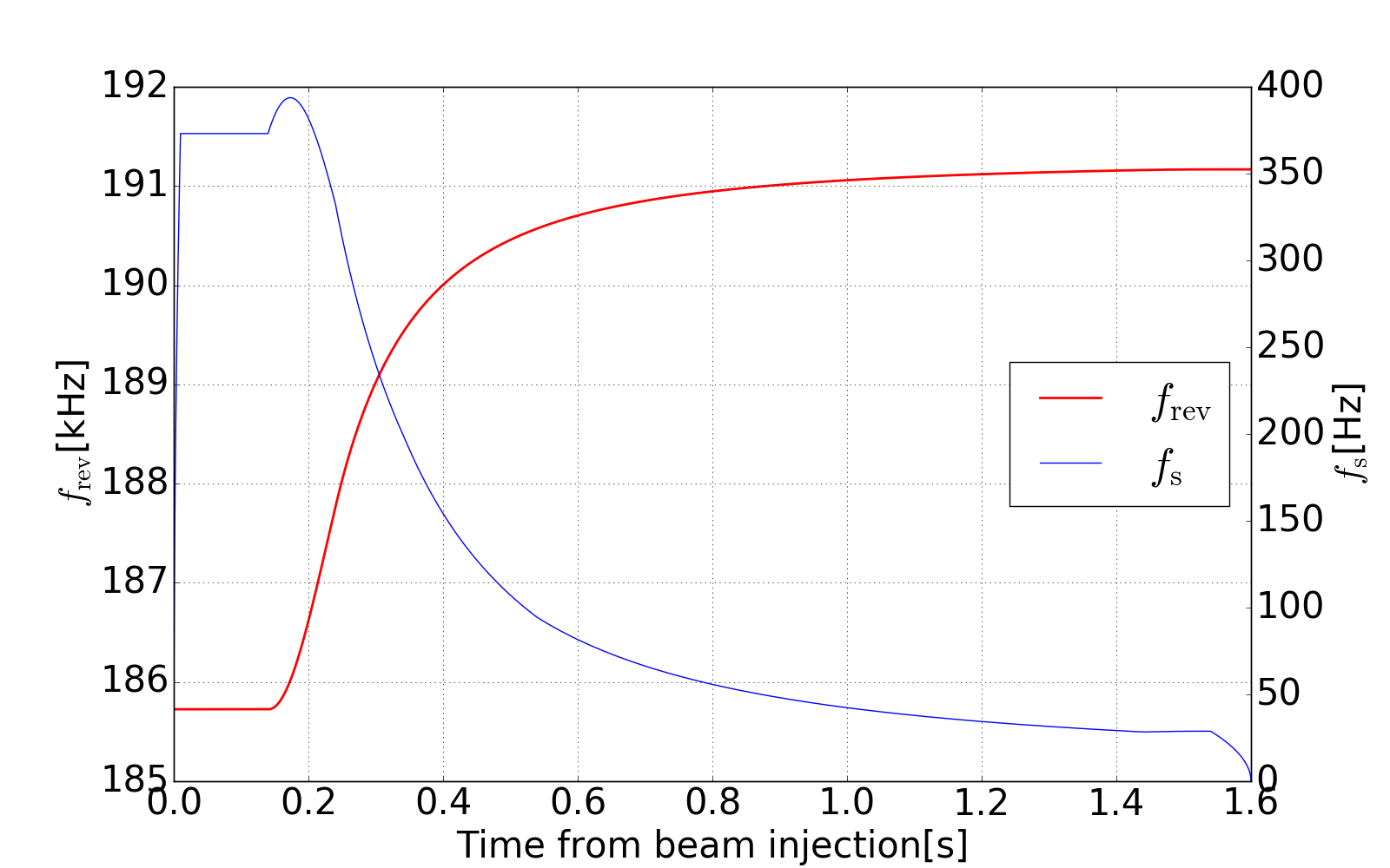
The parameters of the MR and its RF system for the FX are shown in Table I. Figure 1 shows the revolution frequency, , and the synchrotron frequency, , in the MR. During the acceleration from 3 GeV to 30 GeV, the synchrotron frequency is changing largely from 350 Hz at the injection to 30 Hz at the extraction along with the change of the revolution frequency from 185 kHz to 191 kHz.
| parameter | value |
|---|---|
| circumference | 1567.5 m |
| energy | 3–30 GeV |
| beam intensity | (achieved) ppp |
| beam power | (achieved) 500 kW |
| repetition period | 2.48 s |
| accelerating period | 1.4 s |
| accelerating frequency | 1.67–1.72 MHz |
| revolution frequency | 185–191 kHz |
| harmonic number | 9 |
| number of bunches | 8 |
| maximum rf voltage | 320 kV |
| No. of cavities | 7 (h=9), 2 (h=18) |
| Q-value of rf cavity | 22 |
The MR delivers protons per pulse, which corresponds to the beam power of 500 kW, to the neutrino experiment as of May 2018. Large longitudinal bunch oscillation was observed in the MR for the beam power beyond 470 kW[3], and it is necessary to suppress the oscillation for stable beam acceleration at the beam power higher than 500 kW.
I-B Longitudinal Bunch Oscillation in the J-PARC MR
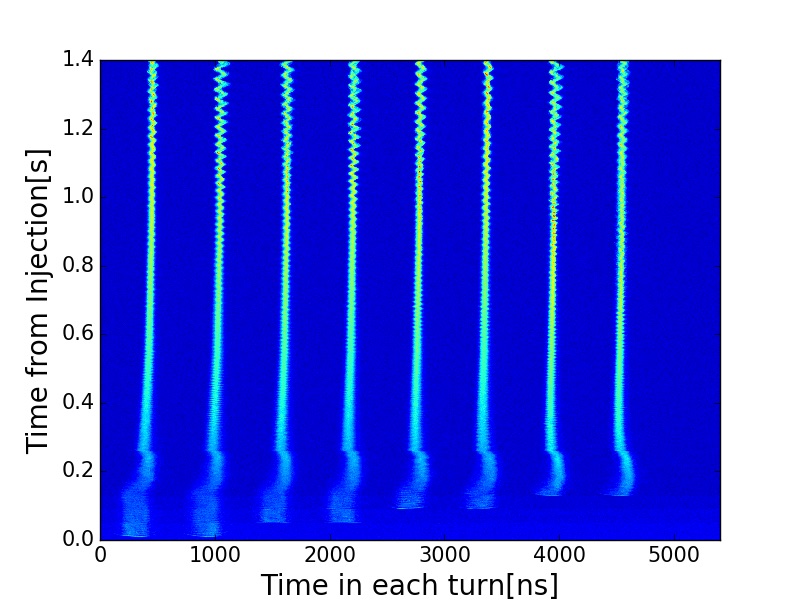
The longitudinal beam oscillation can be seen in a mountain plot. Figure 2 shows the typical mountain plot of the beam signal at the beam power of 480 kW. The beam signal from an Wall Current Monitor (WCM)[4] is recorded by an oscilloscope. The longitudinal dipole oscillation keeps growing from the middle of the acceleration. Each bunch has different amplitude and phase of the dipole oscillation. This kind of the oscillations is called the coupled bunch (CB) oscillation, and the instability caused by the CB oscillation is called the CB instability (CBI).
I-C Coupled Bunch Oscillation
For M bunches, there are M modes of the CB oscillation with the mode number . The CB modes can be seen in the spectrum of the beam signal as synchrotron sidebands of the harmonic components[5]. The frequency of the CB mode can be expressed as follows:
| (1) |
where is the revolution frequency, the synchrotron frequency, and the type of the synchrotron motion. The case with corresponds to the dipole oscillation, and the case with corresponds to the quadruple oscillation. The CB modes appear as the Upper synchrotron Side Bands (USBs) and the Lower synchrotron Side Bands (LSBs) in the cases of and , respectively. Below the accelerating frequency, the LSB and the USB with the CB mode can be expressed as follows:
| (2) | |||||
| (3) |
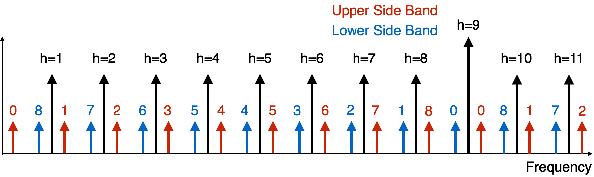
There are 9 CB modes for the MR since the harmonic number of the MR is 9. The spectra of the synchrotron sidebands corresponding to the CB modes in the MR up to the harmonic are illustrated in Fig. 3. There are two sidebands with different CB modes in each harmonic component.
Based on the analysis of the longitudinal CB oscillation [3], strong CB oscillation of mode was observed in the harmonic component of . The suppression of these CB oscillation is a key to achieve the beam power higher than 500 kW.
II Longitudinal Mode-by-Mode Feedback System
To mitigate CB instabilities, we have developed a longitudinal mode-by-mode feedback system.
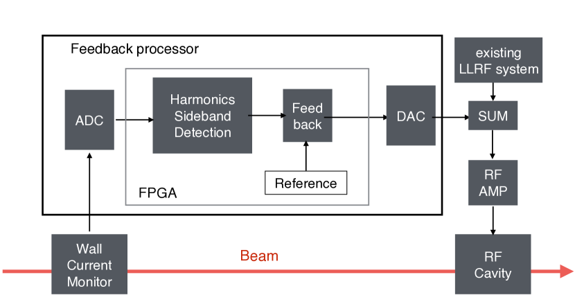
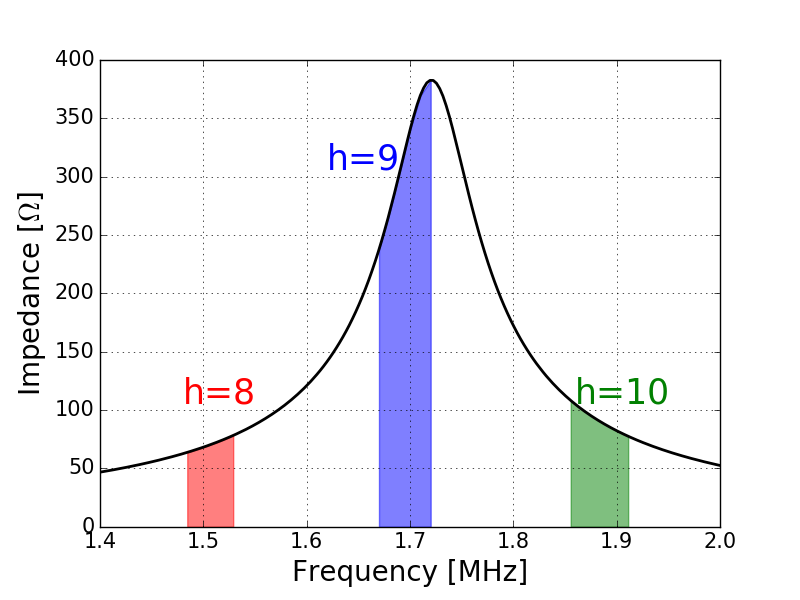
Figure 4 shows the block diagram of the longitudinal mode-by-mode feedback system. The feedback system consists of a WCM, a FPGA-based feedback processor, RF power amplifiers, and a RF cavity as a longitudinal kicker. The beam signal is detected by a WCM and fed to a feedback processor. The feedback processor detects the CB oscillation components of the beam signal and uses it for the feedback control. The detail design of the feedback processor is discussed in the following section. The feedback signal from the feedback processor is led to a high level RF (HLRF) system consisting of power amplifiers and a RF cavity.
The feedback system utilize the existing HLRF system used for the acceleration in the MR. Figure 5 shows the frequency response of the impedance of the RF cavity used for the acceleration in the MR. The RF cavity has impedance large enough to generate the kick voltage for the feedback in the frequency range for component, and can be used as a longitudinal kicker.
The feedback signal from the feedback processor is summed with the RF signal from the existing low level RF (LLRF) system for the acceleration[6]. The summed signal is amplified by the RF power amplifiers and fed into the RF cavity not only to accelerate the beam but also to control the beam oscillation.
III Longitudinal Mode-by-Mode Feedback processor
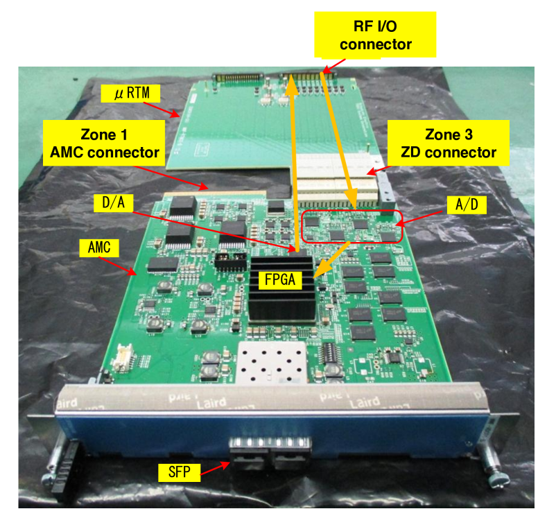
We developed a FPGA-based longitudinal mode-by-mode feedback processor for the feedback system. The feedback processor was manufactured by Mitsubishi Electric TOKKI Systems Corporation based on the MicroTCA.4 architecture.
Figure 6 shows the pictures of the longitudinal mode-by-mode feedback processor. The feedback processor consists of an AMC and a Rear Transition Module (RTM).
The general purpose AMC module[7] developed by Mitsubishi Electric TOKKI Systems Corporation is used in the system. The AMC has 8 ADC channel by 4 ADC111Texas Instruments ADC16DX370 16-bit 370-MSPS ADC chips, 2 DAC channel with a DAC222Analog Devices AD9783 16-bit 500-MSPS DAC chip, and a FPGA. Xilinx Zynq XC7Z045 SoC FPGA is used as a FPGA not only for the signal processing but also for the management of the module itself via EPICS IOC running on the embedded Linux. The 1-GB DDR3-SDRAM on the AMC is used as a pattern memory to store the pattern. A single slot AMC backplane is connected to the AMC to provide the ethernet connection and the power.
The RTM has analog and digital I/O ports and is used as the signal transition module for the AMC. The RTM generates the 144-MHz clock signal for the ADC and the FPGA from the 12-MHz J-PARC master clock by a phase lock loop.
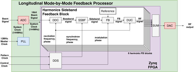
Figure 7 shows the block diagram of the longitudinal mode-by-mode feedback processor. The feedback processor works at a system clock of 144 MHz from the RTM module. The frequency and the phase signals are generated in the Direct Digital Synthesis (DDS) block. The digitized waveform of the beam signal is converted into the baseband signal of each harmonic component by the Digital Down Converter (DDC). and used for the feedback control. The control of each CB mode is achieved by the feedback control of each synchrotron sideband component filtered by the single sideband filter (SSBF)[8]. The outputs of the feedback control are converted to the RF signal by the Digital Up Converter (DUC). The RF signals are summed and converted to the analog signal by the DAC. The feedback processor can process 6 different harmonic components at the same time. The waveforms of the I/Q waveform at each processing stage were recorded and can be acquired via EPICS.
III-A Direct Digital Synthesis
The phase signals used for the signal demodulation and the modulation in the feedback processor are generated by the DDS. The 34-bit phase accumulator generates the phase signal from the frequency signal. The frequency patterns are stored as 32bit words in the DDR3 memory, and loaded from the memory in each pattern clock of 5 kHz. The frequency pattern for the revolution frequency contains the initial frequency as a header word and latter words contains frequency offsets information. The revolution frequency signal is generated by the frequency accumulator which adds the frequency offset to the initial frequency in each control clock of 250 kHz.
III-B Digital Down Converter
The digitized beam signal is down-converted into the baseband I/Q signals of each harmonic component by the DDC.
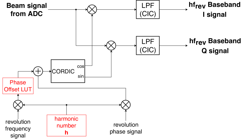
Figure 8 shows the block diagram of the DDC. The digitized beam signal is mixed with the sine and cosine signals of the harmonic frequency. The sine and cosine signals are generated by the CORDIC using the phase signal of the harmonic. The phase signal of the harmonics is generated by multiplying the revolution phase signal with the selected harmonic number. The phase offset to the CORDIC can be set to compensate the phase frequency response of the system. The LUT for the phase offset is addressed by the harmonic frequency.
The mixed signals are led to the Low Pass Filter (LPF) and the baseband I/Q signal is detected. The 5-stage CIC (Cascaded Integrator and Comb) filter is used as a LPF. The CIC filter is running at 144 MHz as the sampling clock. Its decimation ratio is 2 and the differential delay is 256 clocks.
III-C Single Sideband Filter
The LSB and USB are detected separately by the SSBF.
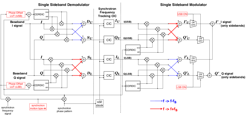
Figure 9 shows the block diagram of the SSBF implemented in the feedback processor.
The I/Q signals of the the harmonics component which contain the synchrotron sidebands are expressed as
| (4) | |||||
| (5) | |||||
where is the synchrotron frequency satisfying , , and the amplitude (phase) of LSB, baseband, and USB components, respectively, and the type of the synchrotron motion.
The I,Q signals are mixed with , , and summed or subtracted to get ,,,:
| (6) | |||||
| (7) | |||||
| (8) | |||||
| (9) | |||||
The harmonic number for the synchrotron frequency can be changed in the feedback processor to select the type of the longitudinal motion. The sine and the cosine signals for mixing are generated by the CORDIC. The phase offset to the CORDIC can be set separately for the LSB and USB to compensate the phase frequency response of the system. The LUT for the phase offset is addressed by the harmonics of the synchrotron frequency.
The I/Q signal of USB(LSB), , for the selected type of the synchrotron motion are obtained by applying a narrow LPF to ,, respectively:
| (10) | |||||
| (11) | |||||
| (12) | |||||
| (13) |
The narrow LPF is required to suppress the sideband component at the harmonics of the synchrotron frequency which changes during the acceleration. In the case of general CIC filter as a LPF, its fixed frequency response changes its performance to suppress these sidebands along with the change of the synchrotron frequency. This means the amount of the remaining sideband component is changed during the acceleration and makes it difficult to control only the selected sideband. To achieve the suppression of these unwanted sidebands for the whole beam cycle, the two-stage frequency tracking CIC filter is used as a narrow LPF. The frequency tracking CIC filter is the CIC filter which changes its notch position along with the frequency pattern. This functionality is achieved by running the CIC filter with 32nd-harmonic of the 1st notch frequency and set its differential delay as 32 clocks. With this setting, the CIC filter has notches at the harmonics of the 1st notch frequency. By setting the synchrotron frequency pattern as the 1st notch frequency of the filter, the filter can always suppress the unwanted sidebands while they change their positions during the acceleration.
The I/Q signals of the LSB and the USB are up-converted to the baseband signal of the harmonic component by mixing with the sinusoidal signal of the synchrotron frequency:
| (14) | |||||
| (15) | |||||
| (16) | |||||
| (17) |
where and are the up-converted I and Q signals of USB(LSB) components, respectively. After up-conversion, I/Q signal of the LSB and the USB are summed as the I/Q signal to the feedback block:
| (18) | |||||
| (19) |
where and are the baseband I/Q signals the harmonic components only with the sideband component. The summation of the LSB and the USB can be disabled individually so that sidebands to be controlled can be selected.
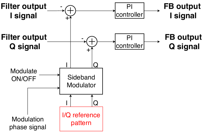
III-D Feedback Control Block
Figure 10 shows the block diagram of the feedback block.
For the feedback control, a Proportional (P) and an Integral (I) controller is implemented in the feedback logic. The P controller runs with the system clock of the 144 MHz and the I controller runs with 250 kHz. The I/Q reference values are loaded from the pattern memory in each pattern clock.
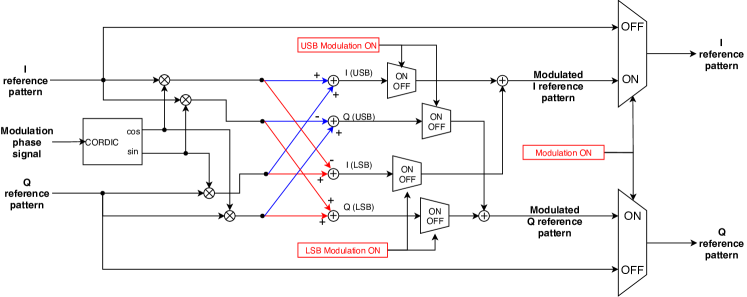
The reference pattern can be modulated with the synchrotron frequency for the beam excitation measurement. Figure 11 shows the block diagram of the modulation block. The reference I/Q pattern is mixed with the sine and the cosine signal of the modulation frequency as same way as that used in the single sideband modulator in the SSBF. The sideband to be excited by the modulation can be selected.
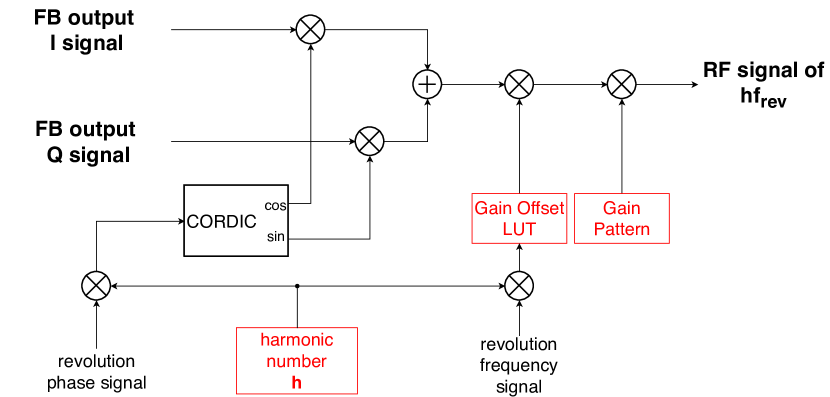
III-E Digital Up Converter
The feedback output is up-converted to a RF signal by the DUC. Figure 12 shows the block diagram of the DUC. The feedback output I/Q signal is mixed with the sine and the cosine signal of the harmonic frequency and summed together as a RF signal. The gain adjustment is done after the up-conversion. The amplitude frequency response of the RF cavity is compensated by the gain LUT addressed by the harmonic frequency. An additional gain control can be done by a gain pattern. The RF signals from all the harmonic blocks are summed and used as the input to the DAC.
IV System Performance Test
IV-A Frequency response
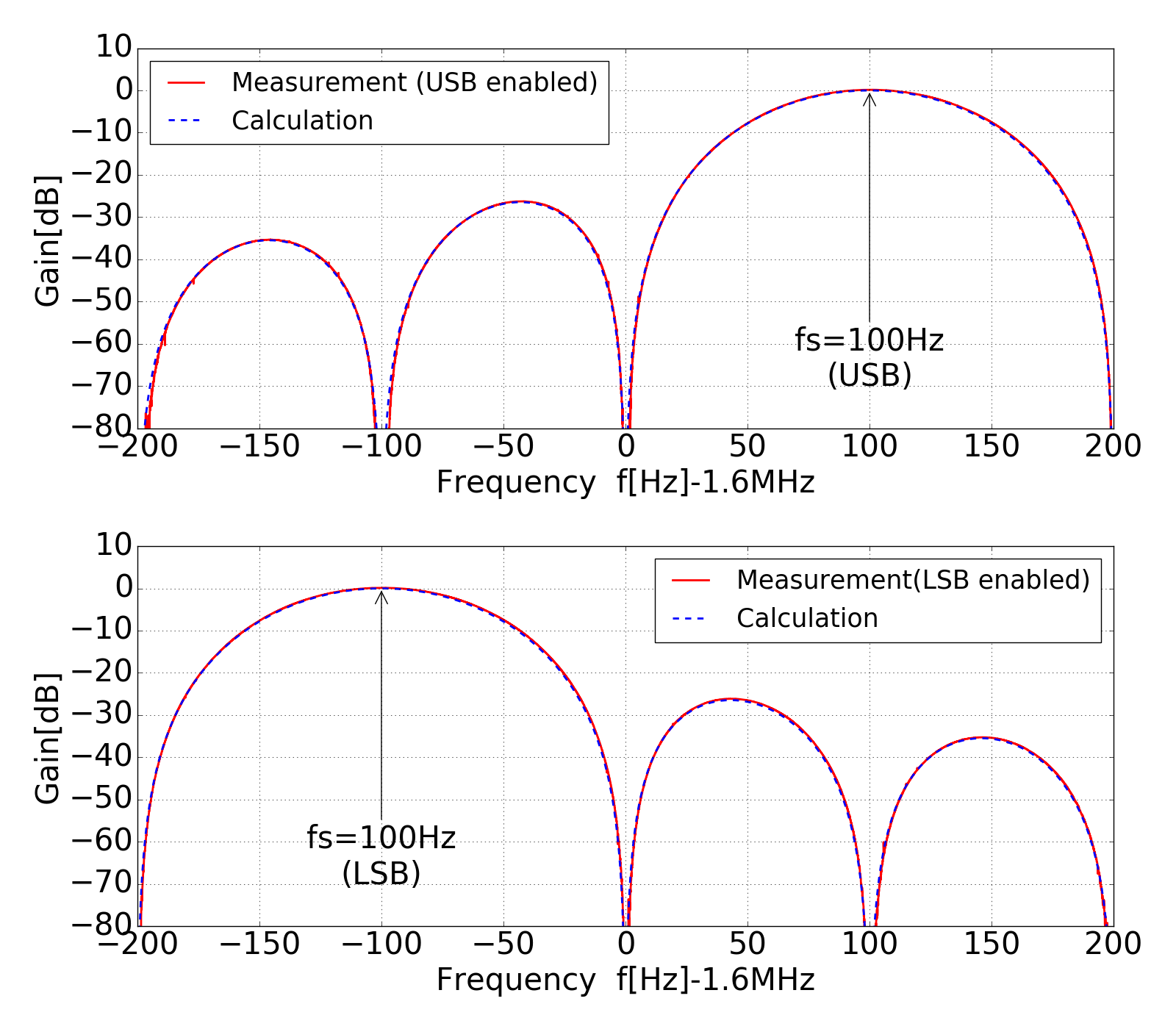
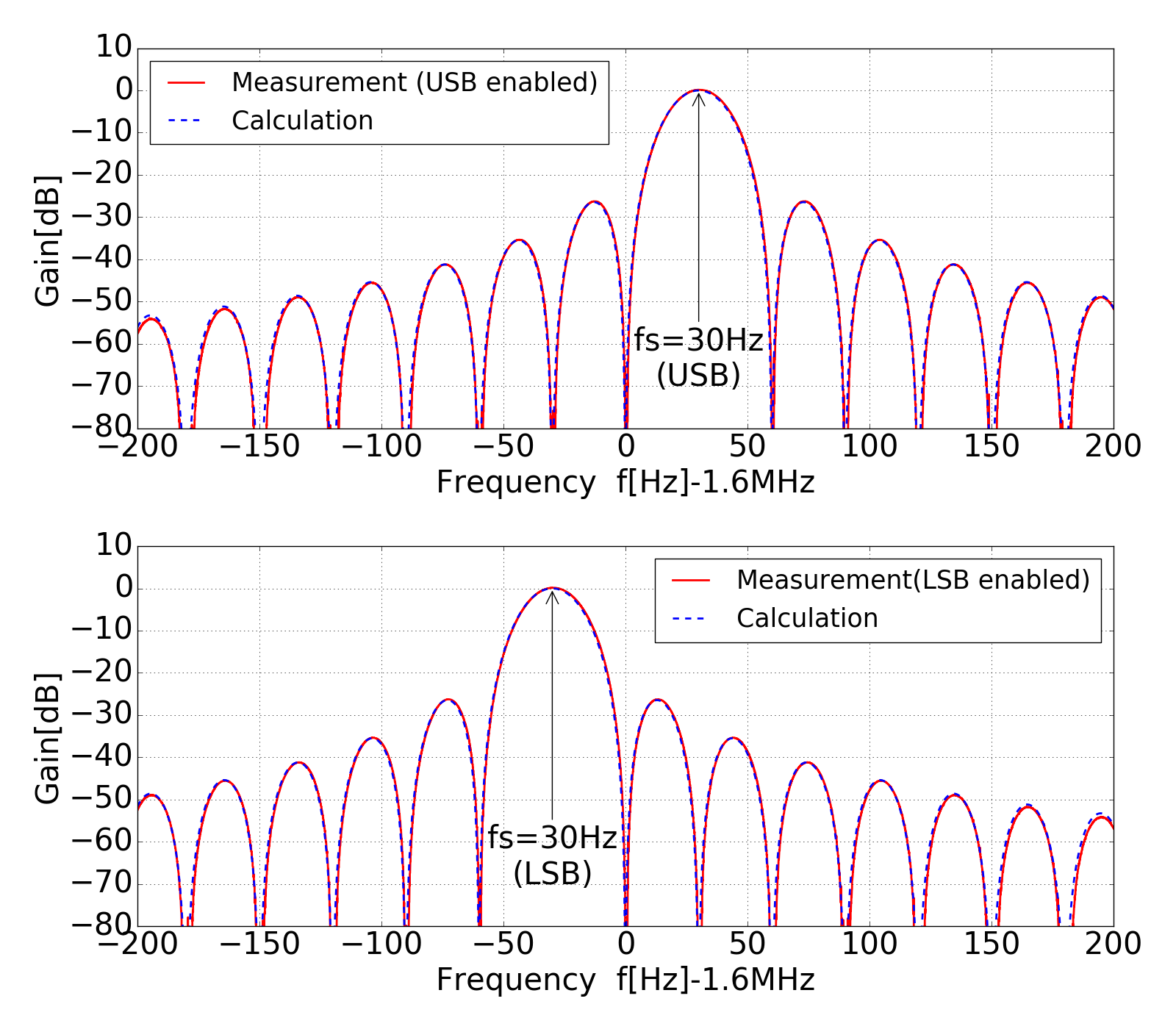
The frequency response of the feedback processor was measured with a network analyzer. The input and the output ports of the feedback processor were connected directly to those of the network analyzer. The revolution frequency pattern was set to 200 kHz with the harmonic number of 8. The gain of the P controller was set to 1 and that of the I controller was set to 0 so that only proportional control was enabled. The reference I/Q pattern was set to to see the frequency response of the filter. The synchrotron frequency pattern was set to constant value for the measurement. Only one sideband was enabled for the output in the SSBF block to see the frequency response of the processor for each sideband.
Figures 13 and 14 show the frequency response of the feedback processor in the case of the synchrotron frequency at 100 Hz and 30 Hz, respectively. In both synchrotron frequency setup, the system had maximum transmission with the gain around 0 dB at the selected sideband frequency, and the DC component and the other sideband component were well suppressed below -80 dB. The measured frequency response matched well with the calculation. This proves that the SSBF worked as designed.
IV-B Measurement of the beam oscillation

The performance of the system to excite and detect the beam oscillation was measured with beam. The measurement was done with the configuration for the beam operation which shown in the Fig. 4. The feedback loop was opened for the measurement. The system kicked the beam with the excitation voltage pattern and monitored the beam oscillation. The excitation voltage pattern was controlled by modulating the I/Q reference pattern. The USB of the harmonic component of was excited by the modulation to have the CB oscillation of mode . The calculated synchrotron frequency pattern was used for the sideband detection and also for the modulation in the feedback processor. A single RF cavity was used in the feedback system to generate the kick voltage of 2.5 kV. The excitation was started from 1.0 sec after the beam injection.
The excitation measurement was done with 12-kW beam low enough to get the stable beam without any longitudinal oscillation. Figure 15 shows the mountain plot for the beam excitation measurement. The beam oscillation growing from 1.0 sec can be seen in this plot. This proves that the system can generate kick voltage large enough to control the beam oscillation.
The oscillation amplitude of each CB mode was obtained by analyzing the motion of bunch centers[9, 3]. The motion of bunch centers were obtained from the analysis of the beam signal recorded by the oscilloscope. Figure 16 shows the variation of the oscillation amplitudes of each CB mode based on the bunch centers motion analysis. No significant CB oscillation observed in all CB modes before the excitation, and only mode has significant growth after the excitation. This result shows that the CB oscillation of mode was successfully excited.

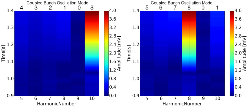
Figure 17 shows the time variation of the amplitudes of the the LSBs and USBs of the harmonic components detected by the feedback processor. The amplitudes of the sidebands were obtained from the recorded waveform of the sideband I/Q complex signal at the output of the CIC filter in the SSBF. The amplitude of the LSBs and USBs of the harmonic component with were recorded. No significant oscillation was observed in any sidebands of monitored harmonic component before the excitation, and only the LSB of component and the USB of the component had significant growth with the excitation. Both sidebands correspond to the CB mode . These sidebands show the similar growth as those measured in the analysis of the oscilloscope data. This result proves that the sideband detection function of the feedback processor worked as expected with the beam.
V Summary and outlook
We summarize the article as follows.
The longitudinal coupled bunch oscillation becomes serious in the J-PARC MR. To mitigate it for stable beam operation with higher beam intensities, we developed a longitudinal mode-by-mode feedback system for the coupled bunch oscillation in the J-PARC MR. The feedback processor detect and control the synchrotron sidebands of each CB mode utilizing the single sideband filter.
The frequency response of the filters in the feedback processor was measured with the network analyzer and was matched well with the calculation. The sideband detection performance of the system was tested with exciting the 12-kW beam. The CB oscillation of the selected mode was successfully excited and the oscillation amplitude of the coupled bunch oscillation measured by the system agreed with the oscilloscope analysis.
We will perform the beam test to suppress the beam oscillation by closing the feedback loop. The measurement of the phase offset LUT with the beam in the feedback loop is a key to close the loop.
Acknowledgments
We would like to thank Heiko Damerau for fruitful discussions on the feedback for the CB instabilities. We also would like to thank the Mitsubishi Electric TOKKI Systems Corporation for their contribution including the hardware and the firmware development for the feedback processor. Finally, we would like to thank all members of the J-PARC accelerator group for their supports.
References
- [1] T. Koseki, Y. Arakaki, Y. H. Chin, K. Hara, K. Hasegawa, Y. Hashimoto, Y. Hori, S. Igarashi, K. Ishii, N. Kamikubota, T. Kimura, K. Koseki, K. Fan, C. Kubota, Y. Kuniyasu, Y. Kurimoto, S. Lee, H. Matsumoto, A. Molodozhentsev, Y. Morita, S. Murasugi, R. Muto, F. Naito, H. Nakagawa, S. Nakamura, K. Niki, K. Ohmi, C. Ohmori, M. Okada, K. Okamura, T. Oogoe, K. Ooya, K. Sato, Y. Sato, Y. Sato, K. Satou, M. Shimamoto, M. Shirakata, H. Someya, T. Sugimoto, J. Takano, Y. Takeda, Y. Takiyama, M. Tejima, M. Toda, M. Tomizawa, T. Toyama, M. Uota, S. Yamada, N. Yamamoto, E. Yanaoka, M. Yoshii, H. Harada, S. Hatakeyama, H. Hotchi, M. Nomura, A. Schnase, T. Shimada, F. Tamura, M. Yamamoto, and T. Shimogawa, “Beam commissioning and operation of the J-PARC main ring synchrotron,” Prog. Theor. Exp. Phys., vol. 2012, no. 1, p. 2B004, 2012. [Online]. Available: http://ptep.oxfordjournals.org/content/2012/1/02B004
- [2] S. Nagamiya, “Introduction to J-PARC,” Prog. Theor. Exp. Phys., vol. 2012, no. 1, p. 2B001, 2012. [Online]. Available: http://ptep.oxfordjournals.org/content/2012/1/02B001
- [3] Y. Sugiyama, F. Tamura, and M. Yoshii, “Measurement of the Longitudinal Coupled Bunch Instabilities in the J-PARC Main Ring,” in Proc. Int. Beam Instrum. Conf. (IBIC’17), Gd. Rapids, MI, USA, 20-24 August 2017, ser. International Beam Instrumentation Conference, no. 6. Geneva, Switzerland: JACoW, 2018, pp. 225–228. [Online]. Available: http://jacow.org/ibic2017/papers/tupcf10.pdf
- [4] T. Toyama, D. Arakawa, Y. Hashimoto, S. Lee, T. Miura, S. Muto, N. Hayashi, R. Toyokawa, and J. Kishiro, “Beam Diagnostics for the J-PARC Main Ring Synchrotron,” in Proc. 2005 Part. Accel. Conf. IEEE, pp. 958–960. [Online]. Available: http://ieeexplore.ieee.org/document/1590624/
- [5] F. Pedersen and F. Sacherer, “Theory and Performance of the Longitudinal Active Damping System for the CERN PS Booster,” IEEE Trans. Nucl. Sci., vol. 24, no. 3, pp. 1396–1398, jun 1977. [Online]. Available: http://ieeexplore.ieee.org/document/4328956/
- [6] F. Tamura, C. Ohmori, M. Yamamoto, M. Yoshii, A. Schnase, M. Nomura, M. Toda, T. Shimada, K. Hasegawa, and K. Hara, “Multiharmonic rf feedforward system for compensation of beam loading and periodic transient effects in magnetic-alloy cavities of a proton synchrotron,” Phys. Rev. Spec. Top. - Accel. Beams, vol. 16, no. 5, p. 051002, may 2013. [Online]. Available: https://link.aps.org/doi/10.1103/PhysRevSTAB.16.051002
- [7] M. Ryoshi, T. Iwaki, K. Tajiri, H. Deguchi, K. Hayashi, R. Matsumoto, and J. Mizuno, “MTCA.4 FPGA(Zynq) A/D·D/A board,” in Proc. 12th Annu. Meet. Part. Accel. Soc. Japan, Tsuruga, 2015, pp. 818–822. [Online]. Available: https://www.pasj.jp/web_publish/pasj2015/proceedings/PDF/WEP1/WEP116.pdf
- [8] B. Kriegbaum and F. Pedersen, “Electronics for the Longitudinal Active Damping System for the CERN PS Booster,” IEEE Trans. Nucl. Sci., vol. 24, no. 3, pp. 1695–1697, jun 1977. [Online]. Available: http://ieeexplore.ieee.org/document/4329055/
- [9] H. Damerau, S. Hancock, C. Rossi, E. Shaposhnikova, J. Tuckmantel, J.-L. Vallet, and M. Mehler, “Longitudinal coupled-bunch instabilities in the CERN PS,” in 2007 IEEE Part. Accel. Conf. IEEE, 2007, pp. 4180–4182. [Online]. Available: http://ieeexplore.ieee.org/document/4439978/