Characterization of a depleted monolithic pixel sensors in 150 nm CMOS technology for the ATLAS Inner Tracker upgrade
Abstract
This work presents a depleted monolithic active pixel sensor (DMAPS) prototype manufactured in the LFoundry 150 nm CMOS process. DMAPS exploit high voltage and/or high resistivity inclusion of modern CMOS technologies to achieve substantial depletion in the sensing volume. The described device, named LF-Monopix, was designed as a proof of concept of a fully monolithic sensor capable of operating in the environment of outer layers of the ATLAS Inner Tracker upgrade in 2025 for the High Luminosity Large Hadron Collider (HL-LHC). This type of devices has a lower production cost and lower material budget compared to presently used hybrid designs. In this work, the chip architecture will be described followed by the characterization of the different pre-amplifier and discriminator flavors with an external injection signal and an iron source (5.9 keV x-rays).
keywords:
Depleted monolithic CMOS active pixel sensor, pixel detector, silicon detector1 Introduction
LF-Monopix chip [1, 2] is the first fully monolithic prototype of Depleted Monolithic Active Pixel Sensors (DMAPS) [3] implemented in the LFoundry 150 nm CMOS technology aimed for high radiation environment. Its design has kept significant features from its ancestor LF-CPIX [4]. The chip size is cm2, where most of the area is occupied by the pixel matrix composed of 36 columns and 129 rows. The pixel size is 250 µm 50 µm. The pixel matrix is not uniform (see Fig. 1) and includes nine pixel flavors (four columns per flavor).
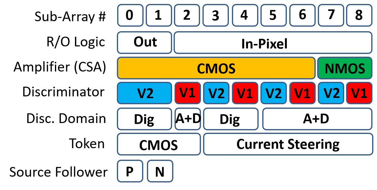
The pixel types are composed of different combinations of pre-amplifier (NMOS or CMOS input), discriminator (a two stage open-loop structure, called V1; and a self-biased differential amplifier with a CMOS output stage, called V2), type of logic gate and placement of in-pixel readout logic. This work describes the characterization of the chip performance of three samples (numbered 7, 11 and 12) in terms of breakdown voltage, gain, input capacitance, threshold dispersion and noise. LF-Monopix chip has also been tested under irradiation [5].
2 Characterization of chip performance
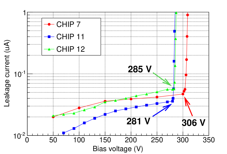
The first measured parameter of LF-Monopix chip is the breakdown voltage, which is the maximum voltage at which the detector can operate. This value is derived from the dependence of the reverse bias voltage applied to the outer P-Well guard rings with the measured leakage current, shown in Fig. 2. Values for breakdown voltage between 280 and 300 V were obtained, much higher than previous chip generation in the same technology [6]. This increase was possible by optimizing the guard ring structure based on TCAD simulations [7].
The gain of different pixels was calibrated using a 55Fe source (5.9 keV x-rays) and monitoring the response of individual pixels in the oscilloscope. For each pixel, the histograms of the signal amplitude and the baseline were generated and their mean values were measured. The pixel gain was then calculated as the ratio of the difference between these mean values and the mean number of ion-electron pairs generated in the substrate (1620 electrons). This procedure was repeated for a minimum of 8 pixels for each flavor. As shown in Table 1, only a dependence on the type of preamplifier was observed. Note that these gain values have to be considered as qualitative, since the real gain of the analogue chip chain is not precisely known. Nevertheless, the signal response of individual pixels can be used to estimate the input capacitance, by calculating the injection signal that gives the same signal response. The values obtained also show a dependence on the type of preamplifier.
| # | Gain (V/e) | Capacitance (fF) | ||
|---|---|---|---|---|
| CMOS | NMOS | CMOS | NMOS | |
| 7 | 15.9 0.1 | 12.0 0.1 | 2.40 0.05 | 2.82 0.05 |
| 12 | 15.5 0.1 | 13.0 0.1 | 2.25 0.06 | 2.47 0.08 |
The threshold distribution and noise level are studied by scanning an external injection signal into the sensing node and recording the probability of pixel firing with a fixed threshold setting (0.795 V), obtaining the so-called “S-curves”. The threshold and noise parameters of each pixel are extracted by fitting an error function to the resulting S-curve. The scan results are shown in Table 2. The threshold level is 2960 (4300) electrons for the V1 (V2) discriminator and its dispersion is 930 (530) electrons. Meanwhile, the noise level is 230 (190) electrons for CMOS (NMOS) preamplifier.
| Feature | Type | Untuned | Tuned |
|---|---|---|---|
| Threshold | V1 discri | 2960 150 | - |
| (e-) | V2 discri | 4290 230 | - |
| Thr. Disp. | V1 discri | 533 45 | 104 14 |
| (e-) | V2 discri | 926 89 | 153 21 |
| Noise | CMOS | 230 17 | 238 17 |
| (e-) | NMOS | 193 10 | 195 13 |
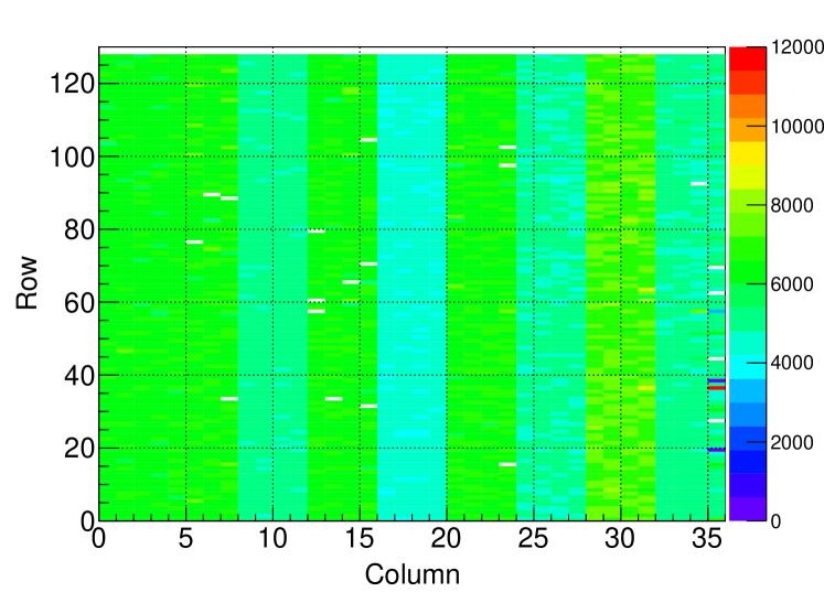
The threshold of each pixel can be independently modified by a 4-bit in-pixel digital-to-analog converter (DAC) called TRIM. Therefore, each pixel was tuned by scanning the TRIM values, determining the corresponding threshold and fitting a linear relation between the TRIM values and the thresholds. Then the optimal TRIM for each pixel is set such as to minimize the threshold dispersion. The result of this procedure is shown for one chip in Fig. 3. The threshold dispersion is reduced down to 150 (100) electrons for the V1 (V2) discriminator, while noise levels remain the same.
3 Summary
The performance of the different flavors of LF-Monopix chip has been characterized with an external injection signal and an iron source. The best results are obtained for the V1 discriminator (threshold dispersion of 100 electrons) and the NMOS preamplifier (noise level of 190 electrons).
Acknowledgments
This work has received funding from the European Union’s Horizon 2020 Research and Innovation programme under Grant Agreements no. 654168 (AIDA 2020) and 675587 (STREAM). F.J. Iguaz acknowledges the support from the Enhanced Eurotalents program (PCOFUND-GA-2013-600382).
References
- [1] T. Wang et al., Development of a Depleted Monolithic CMOS Sensor in a 150 nm CMOS Technology for the ATLAS Inner Tracker Upgrade, JINST 12 (2017) C01039, [1611.01206].
- [2] T. Wang et al., Depleted fully monolithic CMOS pixel detectors using a column based readout architecture for the ATLAS Inner Tracker upgrade, JINST 13 (2018) C03039, [1710.00074].
- [3] I. Peric, A novel monolithic pixelated particle detector implemented in high-voltage CMOS technology, Nucl. Instrum. Meth. A582 (2007) 876–885.
- [4] Y. Degerli et al., Pixel architectures in a HV-CMOS process for the ATLAS inner detector upgrade, JINST 11 (2016) C12064.
- [5] T. Hirono et al., Depleted Fully Monolithic Active CMOS Pixel Sensors (DMAPS) in High Resistivity 150 nm Technology for LHC, 1803.09260.
- [6] T. Hirono et al., CMOS pixel sensors on high resistive substrate for high-rate, high-radiation environments, Nucl. Instrum. Meth. A831 (2016) 94–98.
- [7] J. Liu et al., Simulations of depleted CMOS sensors for high-radiation environments, JINST 12 (2017) C11013.