Band gap and band offset of Ga2O3 and (AlxGa1-x)2O3 alloys
Abstract
Ga2O3 and (AlxGa1-x)2O3 alloys are promising materials for solar-blind UV photodetectors and high-power transistors. Basic key parameters in the device design, such as band gap variation with alloy composition and band offset between Ga2O3 and (AlxGa1-x)2O3, are yet to be established. Using density functional theory with the HSE hybrid functional, we compute formation enthalpies, band gaps, and band edge positions of (AlxGa1-x)2O3 alloys in the monoclinic () and corundum () phases. We find the formation enthlapies of (AlxGa1-x)2O3 alloys are significantly lower than of (InxGa1-x)2O3, and that (AlxGa1-x)2O3 with =0.5 can be considered as an ordered compound AlGaO3 in the monoclinic phase, with Al occupying the octahedral sites and Ga occupying the tetrahedral sites. The band gaps of the alloys range from 4.69 to 7.03 eV for -(AlxGa1-x)2O3 and from 5.26 to 8.56 eV for -(AlxGa1-x)2O3. Most of the band offset of the (AlxGa1-x)2O3 alloy arises from the discontinuity in the conduction band. Our results are used to explain the available experimental data, and consequences for designing modulation-doped field effect transistors (MODFETs) based on (AlxGa1-x)2O3/Ga2O3 are discussed.
Ga2O3 has been intensively investigated as a wide-band-gap semiconductor for high-power electronics Higashiwaki et al. (2012); Masataka et al. (2016); Jessen et al. (2017) and UV solar-blind phtodetectors Oshima et al. (2008, 2007). It is available as large single crystals Aida et al. (2008) suitable for high-quality epitaxial thin-film growth by metalorganic chemical vapor deposition (MOCVD) Du et al. (2015); Baldini et al. (2017) and molecular beam epitaxy (MBE) Víllora et al. (2006); Oshima et al. (2007); It displays high breakdown electric field Higashiwaki et al. (2012), and the Baliga figure of merit exceeds that of SiC and GaN Jessen et al. (2017); It can be easily doped -type, and band gap engineering can be accomplished by incorporating In and Al, adding great flexibility to device design. Modulation doping of (AlxGa1-x)2O3/Ga2O3 heterostructures can be used to separate the ionized donors in the (AlxGa1-x)2O3 layer from the conduction electrons in the Ga2O3 layer Krishnamoorthy et al. (2017); Oshima et al. (2017); Ahmadi et al. (2017); Kang et al. (2017), providing a boost to the electron mobility to about 500 cm2V-1s-1 Ma et al. (2016); Zhang et al. (2018); Krishnamoorthy et al. (2017) by suppressing scattering from the ionized impurities. Simulated band diagrams and two-dimension electron gas (2DEG) profile of MODFETs based on (AlxGa1-x)2O3/Ga2O3 assumed that the discontinuity in the band offset appears solely on the conduction band Krishnamoorthy et al. (2017). However this assumption has not been based on firm experimental evidence or first-principles calculations. The band gap of the (AlxGa1-x)2O3 alloy and the band offset between the (AlxGa1-x)2O3 and Ga2O3 are key parameters in the device design and are yet to be established.
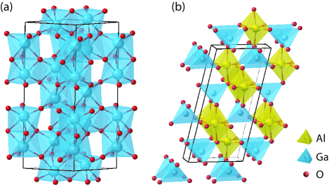
Ga2O3 and (AlxGa1-x)2O3 can be made in the monoclinic () and in the corundum () phase, as shown in Fig. 1. Bulk and thin films of -(AlxGa1-x)2O3 have been obtained using solution combustion synthesis Krueger et al. (2016), pulsed laser deposition (PLD) Zhang et al. (2014), and oxygen plasma-assisted molecular beam epitaxy (MBE) Krishnamoorthy et al. (2017); Oshima et al. (2017); Ahmadi et al. (2017), while -(AlxGa1-x)2O3 have been grown on sapphire substrates by chemical vapor deposition (CVD) for Al content of up to 81% Ito et al. (2012); Uchida et al. (2016). Band gaps of (AlxGa1-x)2O3 for selected Al content have been reported Ito et al. (2012); Uchida et al. (2016); Krueger et al. (2016); Zhang et al. (2014); Feng et al. (2017), but band offsets between Ga2O3 and (AlxGa1-x)2O3, which are much more challenging to obtain experimentally, are still unknown.
Using density functional theory and the HSE hybrid functional, we investigate the formability of (AlxGa1-x)2O3 alloys in both and phases, their band gaps as a function of Al concentration, and the band offsets of the (AlxGa1-x)2O3 alloys with respect to Ga2O3 and Al2O3. In the following, we first describe the details of the calculations, present the results for structural parameters and stability of the alloys, and then discuss the results for band gaps and band offsets for both and phases and the implications for device design.
| -Al2O3 | -Al2O3 | -Ga2O3 | -Ga2O3 | |||||
|---|---|---|---|---|---|---|---|---|
| Calc. | Expt. | Calc. | Expt. | Calc. | Expt. | Calc. | Expt. | |
| (Å) | 4.774 | 4.76 11footnotemark: 1 | 11.808 | 11.795 22footnotemark: 2 | 5.005 | 4.983 33footnotemark: 3 | 12.276 | 12.214 44footnotemark: 4 |
| (Å) | 2.921 | 2.910 22footnotemark: 2 | 3.050 | 3.037 44footnotemark: 4 | ||||
| (Å) | 13.013 | 12.99 11footnotemark: 1 | 5.636 | 5.621 22footnotemark: 2 | 13.454 | 13.433 33footnotemark: 3 | 5.811 | 5.798 44footnotemark: 4 |
| (deg) | 104.08 | 103.79 22footnotemark: 2 | 103.72 | 103.83 44footnotemark: 4 | ||||
| (eV/f.u.) | -15.753 | -16.971 55footnotemark: 5 | -15.561 | -9.824 | -9.870 | -11.30 66footnotemark: 6 | ||
| (eV) | 8.56 (d) | 8.8 77footnotemark: 7 | 7.03 (i) | 5.26 (i) | 5.3 88footnotemark: 8 | 4.69 (i) | 4.48 99footnotemark: 9, 4.9 1010footnotemark: 10 | |
The calculations are based on the density functional theory (DFT) Hohenberg and Kohn (1964); Kohn and Sham (1965) with the projector augmented-wave method (PAW) Blöchl (1994) as implemented in the VASP code Kresse and Hafner (a, b). The states of Ga are included as valence states, and a plane-wave cutoff energy of 400 eV is employed. We use Perdew-Burke-Ernzerhof functional revised for solids (PBEsol) Perdew et al. (2008) to relax all structures. To overcome the severe underestimation of band gaps in the DFT-PBEsol functional, we employed the screened hybrid functional of Heyd, Scuseria, and Ernzerhof (HSE06) Heyd et al. (2003, 2006). In the HSE hybrid functional, the nonlocal Hartree-Fock exchange is mixed with the generalized gradient approximation (GGA) Perdew et al. (1996) exchange in the short-range part. The mixing parameter in HSE is fixed to 32% for all the calculations. We find that this choice of mixing parameter gives band gaps of the parent compounds Ga2O3 and Al2O3 in good agreement with experimental values. Note that, conventionally, monoclinic Al2O3 is often denoted as the phase in the literature, i.e., -Al2O3 shares the same crystal structure as -Ga2O3 Yamaguchi et al. (1970); Zhou and Snyder (1991); Husson and Repelin (1996). The calculated lattice parameters, formation enthalpies, and band gaps for Al2O3 and Ga2O3 are listed in Table 1 along with the available experimental data. The -Al2O3, -Ga2O3, and -Ga2O3 have indirect gaps where the valence-band maximum is higher than the valence-band edge at by 0.16, 0.24, and 0.04 eV, respectively, as previously reported Peelaers and Van de Walle (2015).
We simulate (AlxGa1-x)2O3 random alloys using special quasirandom structures (SQS) Zunger et al. (1990) generated using the mcsqs code of the Alloy Theoretic Automated Toolkit (ATAT) van de Walle et al. (2013). This method can generate optimal periodic supercells comparable to true disordered structures based on a Monte Carlo simulated annealing loop with an objective function that seeks to perfectly match the maximum number of correlation functions van de Walle et al. (2013).
We use supercells containing 80 atoms for the and 120 atoms for the phase. In the case of -Ga2O3, all Ga sites are equivalent; therefore, Al tends to replace Ga randomly. However, in the case of -Ga2O3, half of Ga atoms are at octahedral sites and the other half at tetrahedral sites. We find that Al strongly prefers octahedral sites, i.e., Al sitting at octahedral sites is 0.2 eV per Al atom lower in energy than Al sitting at tetrahedral sites. Therefore, in the generation of SQS structures to simulate -(AlxGa1-x)2O3 alloys, we assumed that Al atoms occupy only octahedral sites for . For , Al atoms exceeding randomly replace Ga at tetrahedral sites since all octahedral sites are already filled.
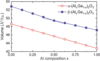
Figure 2 shows the calculated equilibrium volume of (AlxGa1-x)2O3 alloys as a function of Al fraction. For -(AlxGa1-x)2O3, the volume varies linearly with Al composition, following Vegard’s law. For -(AlxGa1-x)2O3, the volume also decreases monotonically with Al fraction, but exhibit a change in slope at . This discontinuity in the slope is attributed to Al occupying the tetrahedral sites for . This trend was recently observed by Krueger et al. Krueger et al. (2016)
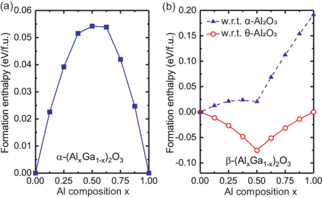
The calculated formation enthalpies of Ga2O3 and Al2O3, defined as the total energy of the compound minus the total energies of the elemental bulk phases, are listed in Table 1. We find that the formation enthalpy of -Ga2O3 is only 46 meV/f.u. higher than -Ga2O3. In contrast, -Al2O3 is much more stable than -Al2O3, by 192 meV/f.u. This is again attributed to the preference of Al occupying octahedral sites, by eV per cation. Figure 3(a) and (b) show the formation enthalpies of and -(AlxGa1-x)2O3, defined as:
| (1) |
where is the total energy of the SQS supercell structure representing the random alloy, and and are the total energies of the parent compounds Ga2O3 and Al2O3 in the same supercell. The formation enthalpies of -(AlxGa1-x)2O3 are relatively small compared to other alloys. For example, at , the formation enthalpy of -(InxGa1-x)2O3 is 300 meV/f.u.Peelaers et al. (2015), compared to 55 meV/f.u. for (AlxGa1-x)2O3. This indicates that -(AlxGa1-x)2O3 alloys are more likely to form at all Al compositions. In the case of -(AlxGa1-x)2O3, we find a stable ordered compound AlGaO3 for 50% Al content. If taken with respect to - (dashed line), which is the most stable phase of , the formation enthalpy of -(AlxGa1-x)2O3 rapidly increases with Al composition above 50%. Again, this is explained by the fact that Al strongly prefer to occupy the octahedral sites for , but endup occupying the only available tetrahedral sites for .
Therefore, for Al concentrations approaching 100%, we predict that (AlxGa1-x)2O3 alloys strongly favor the corundum or phase. This explains why single monoclinic phase at and mixed corundum and monoclinic phases for have been observed by solution combustion synthesis Krueger et al. (2016). We note, however, that thin films of -(AlxGa1-x)2O3 alloys with Al content up to 96% have been reported using pulsed laser deposition (PLD) Zhang et al. (2014).
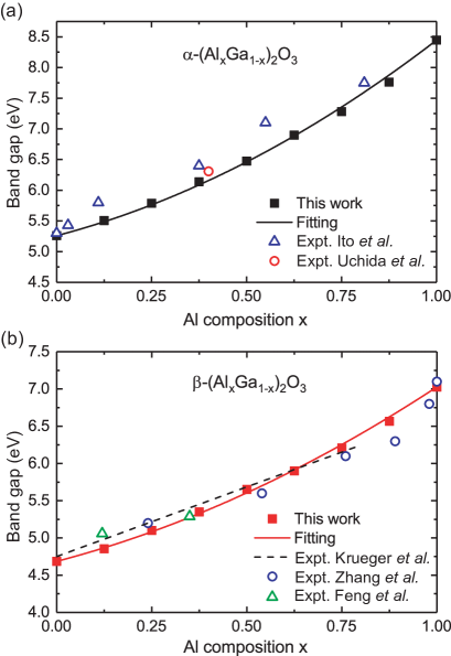
The calculated band gap of (AlxGa1-x)2O3 alloys as a function of Al content is shown in Fig. 4. The band-gap bowing parameter is derived by fitting the results using:
| (2) |
We obtained a bowing parameter of 1.6 eV for and 1.0 eV for the -(AlxGa1-x)2O3 alloys. Overall, our results are in good agreement with the available experimental data Ito et al. (2012); Uchida et al. (2016); Krueger et al. (2016); Zhang et al. (2014); Feng et al. (2017), also shown in Figure 4. Due to the stability of the ordered AlGaO3 (), we can define two independent bowing parameters, one for and another for . These are listed in the Supplemental Material along the bowing parameters for the VBM and CBM separatelysup .
The band offsets between (AlxGa1-x)2O3 and the parent compound Ga2O3 are crucial parameters in the design of electronic devices that depend on carrier confinement or on the separation between carriers and ionized impurities such as in modulation-doped field-effect transistors (MODFETs) Krishnamoorthy et al. (2017); Zhang et al. (2018). We calculated the band offset between two materials using the following procedure Janotti and Van de Walle (2007). First, the valence-band maximum (VBM) and the conduction-band minimum (CBM) of the bulk materials are determined with respect to the averaged electrostatic potential. Then we align the averaged electrostatic potential in the two materials by performing an an interface calculation. In this case, we used supercells composed of 12 layers of each material with two equivalent interfaces. The supercells are constructed along non-polar directions to avoid problems resulting from the polar discontinuity at the interface and the consequent slopes in the averaged electrostatic potential in the bulk regions. For Ga2O3 and Al2O3 in the monoclinic phase, we chose a superlattice geometry along the [010] non-polar direction. For the corundum phase, we constructed a superlattice along the [100] non-polar direction. To avoid the problem of lattice mismatch, we used average in-plane lattice parameters; the out-of-plane lattice parameter is set so that each material in the superlattice has its equilibrium volume. In this way, the averaged electrostatic potentials in each side of the interface correspond the average electrostatic potential in the respective bulk materials. This procedure, therefore, gives us the natural band offset between Ga2O3 and Al2O3.
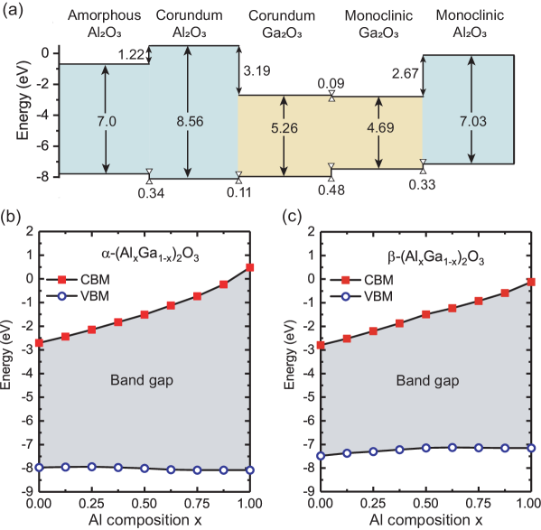
For monoclinic Ga2O3 and Al2O3, we find a type II staggered alignment, with a valence-band offset of 0.33 eV and a conduction-band offset of 2.67 eV, as shown in Fig. 5(a). Thus, 89% of the band offset arrises from the discontinuity in the conduction band, and only 11% comes from the valence band. In the case of corundum Ga2O3 and Al2O3, we find a type I straddling alignment, with 0.11 eV valence-band offset and 3.19 eV conduction-band offset, also shown in Fig. 5(a), i.e., 97% of the offset comes from the conduction band, and only 3% from the valence band.
We also determined the absolute position of the valence and conduction bands by taking the averaged electrostatic potential of and -Ga2O3 with respect to the vacuum level using surface calculations of non-polar terminations. The results are shown in the energy axis of Fig. 5(a), where we also added the band-edge positions of amorphous Al2O3 according to previous experimental results of band gap and valence-band offset with -Al2O3 from Ref. Filatova and Konashuk, 2015 for comparison.
Finally, we determined the band-edge positions in (AlxGa1-x)2O3 with respect to that in Ga2O3 and Al2O3. The averaged electrostatic potential for a given alloy composition is derived from a linear interpolation of the averaged electrostatic potential of the constituents compounds. Figure 5(b) and (c) show the derived VBM and CBM positions for and -(AlxGa1-x)2O3 as a function of Al composition. The valence-band edges only change slightly with Al concentration , while most of the change occurs in the CBM. This is expected since O 2 states dominate the VBM. All the band gap values, the absolute position of VBM and CBM, and the corresponding bowing parameters are listed in the Supplemental Material sup .
The results above have important implications to device design. For instance, for Al concentration of 20% we find that the conduction-band offset between monoclinic (Al0.2Ga0.8)2O3 and Ga2O3 of 0.47 eV, compared to the assumed 0.6 eV in Ref.Krishnamoorthy et al., 2017 for a MODFET structure. This relatively small conduction-band offset for 20% Al content in the alloy can be insufficient so that electrons from the 2DEG at the (Al0.2Ga0.8)2O3/Ga2O3 may stay in the Si -doped layer in the (Al0.2Ga0.8)2O3 alloy, causing a parasitic parallel channel of conduction in the MODFET Krishnamoorthy et al. (2017). Higher Al concentrations in the (AlxGa1-x)2O3 film (AlxGa1-x)2O3, resulting in increased conduction-band offsets, are required to overcome this detrimental effect.
We also note the discontinuity in the first-order derivative for the CBM and VBM at for -(AlxGa1-x)2O3. Like the discontinuities in volume and formation enthalpies, this is attributed to Al also occupying tetrahedral sites for . The kinks at in the equilibrium volume, formation enthalpies, and band-edge positions of (AlxGa1-x)2O3 indicate that -AlGaO3 may well be considered an ordered compound with Al in octahedral sites and Ga in tetrahedral sites instead of a random alloy.
In summary, we find that (AlxGa1-x)2O3 alloys have much lower mixing enthalpies than (InxGa1-x)2O3. The band gap of the alloys can be tuned in a wide range by changing Al composition, adding great flexibility in the design of (AlxGa1-x)2O3/Ga2O3-based electronic devices. The conduction-band discontinuity comprises 89% of the band offset between monoclinic Al2O3 and Ga2O3, and 97% in the case of the corundum phase. Our results suggest that films with Al concentrations larger that 20% are required to avoid unwanted parallel conduction channel in MODFETs based on monoclinic (AlxGa1-x)2O3/Ga2O3 heterostructures.
Acknowledgements
T.W. and C.N. were supported by the II-VI Foundation, and A.J. was supported by the National Science Foundation Grant No. DMR-1652994. This research was supported through the use of the Extreme Science and Engineering Discovery Environment (XSEDE) supercomputer facility, National Science Foundation grant number ACI-1053575, and the Information Technologies (IT) resources at the University of Delaware, specifically the high-performance computing resources.
References
- Higashiwaki et al. (2012) Masataka Higashiwaki, Kohei Sasaki, Akito Kuramata, Takekazu Masui, and Shigenobu Yamakoshi, “Gallium oxide (Ga2O3) metal-semiconductor field-effect transistors on single-crystal -Ga2O3 (010) substrates,” Appl. Phys. Lett. 100, 013504 (2012).
- Masataka et al. (2016) Higashiwaki Masataka, Sasaki Kohei, Murakami Hisashi, Kumagai Yoshinao, Koukitu Akinori, Kuramata Akito, Masui Takekazu, and Yamakoshi Shigenobu, “Recent progress in Ga2O3 power devices,” Semicond. Sci. Technol. 31, 34001 (2016).
- Jessen et al. (2017) G. Jessen, K. Chabak, A. Green, J. McCandless, S. Tetlak, K. Leedy, R. Fitch, S. Mou, E. Heller, S. Badescu, A. Crespo, and N. Moser, “Toward realization of Ga2O3 for power electronics applications,” in Device Res. Conf., Vol. 75th Annua (2017) pp. 1–2.
- Oshima et al. (2008) Takayoshi Oshima, Takeya Okuno, Naoki Arai, Norihito Suzuki, Shigeo Ohira, and Shizuo Fujita, “Vertical solar-blind deep-ultraviolet schottky photodetectors based on -Ga2O3 substrates,” Appl. Phys. Express 1, 011202 (2008).
- Oshima et al. (2007) Takayoshi Oshima, Takeya Okuno, and Shizuo Fujita, “Ga2O3 thin film growth on -plane sapphire substrates by molecular beam epitaxy for deep-ultraviolet photodetectors,” Jpn. J. Appl. Physics 46, 7217–7220 (2007).
- Aida et al. (2008) Hideo Aida, Kengo Nishiguchi, Hidetoshi Takeda, Natsuko Aota, Kazuhiko Sunakawa, and Yoichi Yaguchi, “Growth of -Ga2O3 single crystals by the edge-defined, film fed growth method,” Jpn. J. Appl. Phys. 47, 8506–8509 (2008).
- Du et al. (2015) Xuejian Du, Zhao Li, Caina Luan, Weiguang Wang, Mingxian Wang, Xianjin Feng, Hongdi Xiao, and Jin Ma, “Preparation and characterization of Sn-doped -Ga2O3 homoepitaxial films by MOCVD,” J. Mater. Sci. 50, 3252–3257 (2015).
- Baldini et al. (2017) Michele Baldini, Martin Albrecht, Andreas Fiedler, Klaus Irmscher, Robert Schewski, and Günter Wagner, “Editors Choice: Si- and Sn-Doped Homoepitaxial -Ga2O3 Layers Grown by MOVPE on (010)-Oriented Substrates,” ECS J. Solid State Sci. Technol. 6, Q3040–Q3044 (2017).
- Víllora et al. (2006) Encarnación G. Víllora, Kiyoshi Shimamura, Kenji Kitamura, and Kazuo Aoki, “Rf-plasma-assisted molecular-beam epitaxy of -Ga2O3,” Appl. Phys. Lett. 88, 031105 (2006).
- Krishnamoorthy et al. (2017) Sriram Krishnamoorthy, Zhanbo Xia, Chandan Joishi, Yuewei Zhang, Joe Mcglone, Jared Johnson, Aaron R Arehart, Jinwoo Hwang, Saurabh Lodha, Siddharth Rajan, Sriram Krishnamoorthy, Zhanbo Xia, Chandan Joishi, Yuewei Zhang, Saurabh Lodha, and Siddharth Rajan, “Modulation-doped -(Al0.2Ga0.8)2O3/Ga2O3 field-effect transistor,” Appl. Phys. Lett. 111, 023502 (2017).
- Oshima et al. (2017) Takayoshi Oshima, Yuji Kato, Naoto Kawano, Akito Kuramata, Shigenobu Yamakoshi, Shizuo Fujita, Toshiyuki Oishi, and Makoto Kasu, “Carrier confinement observed at modulation-doped -(AlxGa1−x)2O3/Ga2O3 heterojunction interface,” Appl. Phys. Express 10, 035701 (2017).
- Ahmadi et al. (2017) Elaheh Ahmadi, Onur S Koksaldi, Xun Zheng, Tom Mates, Yuichi Oshima, Umesh K Mishra, and James S. Speck, “Demonstration of -(AlxGa1−x)2O3/-Ga2O3 modulation doped field-effect transistors with Ge as dopant grown via plasma-assisted molecular beam epitaxy,” Appl. Phys. Express 10, 071101 (2017).
- Kang et al. (2017) Youngho Kang, Karthik Krishnaswamy, Hartwin Peelaers, and Chris G Van de Walle, “Fundamental limits on the electron mobility of -Ga2O3,” J. physics. Condens. matter 29, 234001 (2017).
- Ma et al. (2016) Nan Ma, Nicholas Tanen, Amit Verma, Zhi Guo, Tengfei Luo, Huili (Grace) Xing, and Debdeep Jena, “Intrinsic electron mobility limits in -Ga2O3,” Appl. Phys. Lett. 109, 212101 (2016).
- Zhang et al. (2018) Yuewei Zhang, Adam Neal, Zhanbo Xia, Chandan Joishi, Yuanhua Zheng, Sanyam Bajaj, Mark Brenner, Shin Mou, Donald Dorsey, Kelson Chabak, Gregg Jessen, Jinwoo Hwang, Joseph Heremans, and Siddharth Rajan, “High Mobility two-dimensional electron gas in modulation-doped -(AlxGa1-x)2O3/Ga2O3 heterostructures,” Appl. Phys. Lett. 112, 173502 (2018).
- Krueger et al. (2016) Benjamin W Krueger, Christopher S Dandeneau, Evan M Nelson, Scott T Dunham, Fumio S Ohuchi, and Marjorie A Olmstead, “Variation of Band Gap and Lattice Parameters of -(AlxGa1-x)2O3 Powder Produced by Solution Combustion Synthesis,” J. Am. Ceram. Soc. 99, 2467–2473 (2016).
- Zhang et al. (2014) Fabi Zhang, Katsuhiko Saito, Tooru Tanaka, Mitsuhiro Nishio, Makoto Arita, and Qixin Guo, “Wide bandgap engineering of (AlGa)2O3 films,” Appl. Phys. Lett. 105, 162107 (2014).
- Ito et al. (2012) Hiroshi Ito, Kentaro Kaneko, and Shizuo Fujita, “Growth and Band Gap Control of Corundum-Structured -(AlGa)2O3 Thin Films on Sapphire by Spray-Assisted Mist Chemical Vapor Deposition,” Jpn. J. Appl. Phys. 51, 100207 (2012).
- Uchida et al. (2016) Takayuki Uchida, Riena Jinno, Shu Takemoto, Kentaro Kaneko, and Shizuo Fujita, “Characterization of band offset in -(AlxGa1-x)2O3/-Ga2O3 heterostructures,” in 2016 Compd. Semicond. Week, Vol. 113 (2016) pp. 5–6.
- Feng et al. (2017) Qian Feng, Xiang Li, Genquan Han, Lu Huang, Fuguo Li, Weihua Tang, Jincheng Zhang, and Yue Hao, “(AlGa)2O3 solar-blind photodetectors on sapphire with wider bandgap and improved responsivity,” Opt. Mater. Express 7, 1240–1248 (2017).
- Yamaguchi et al. (1970) Goro; Yamaguchi, Itaru; Yasui, and Wen-Chau Chiu, “A New Method of Preparing Theta-Alumina and the Interpretation of its X-ray power Diffraction Pattern and Electron Diffraction Pattern,” Bull. Chem. Soc. Japan 43, 2487–2491 (1970).
- Zhou and Snyder (1991) Rong-Sheng Zhou and Robert L. Snyder, “Structures and transformation mechanisms of the , and transition aluminas,” Acta Crystallogr. B B47, 617–630 (1991).
- Husson and Repelin (1996) E Husson and Y Repelin, “Structural studies of transition aluminas. Theta alumina,” Eur. J. solid state Inorg. Chem. 33, 1223–1231 (1996).
- Newnham and De Haan (1962) E E Newnham and Y M De Haan, “Refinement of the Al2O3, Ti2O3, V2O3 and Cr2O3 structures,” Zeitschrift für Krist. Mater. 117, 235–237 (1962).
- Marezio and Remeika (1967) M Marezio and J P Remeika, “Bond Lengths in the -Ga2O3 Structure and the Highâ€Pressure Phase of Ga2−xFexO3,” J. Chem. Phys. 46, 1862–1865 (1967).
- Åhman et al. (1996) John Åhman, Göran Svensson, and Jörgen Albertsson, “A reinvestigation of -gallium oxide,” Acta Crystallogr. 52, 1336–1338 (1996).
- Ghosh and Kay (1977) D Ghosh and D A R Kay, “Standard free energy of formation of alumina,” J. Electrochem. Soc. 124, 1836–1845 (1977).
- Barin (2008) Ihsan Barin, “Ga-Ge5U3,” in Thermochem. Data Pure Subst. (Wiley-VCH Verlag GmbH, 2008) pp. 728–780.
- French (1990) Roger H French, “Electronic Band Structure of Al2O3, with Comparison to Alon and AIN,” J. Am. Ceram. Soc. 73, 477–489 (1990).
- Shinohara and Fujita (2008) Daisuke Shinohara and Shizuo Fujita, “Heteroepitaxy of Corundum-Structured -Ga2O3 Thin Films on -Al2O3 Substrates by Ultrasonic Mist Chemical Vapor Deposition,” Jpn. J. Appl. Phys. 47, 7311 (2008).
- Onuma et al. (2015) Takeyoshi Onuma, Shingo Saito, Kohei Sasaki, Tatekazu Masui, Tomohiro Yamaguchi, Tohru Honda, and Masataka Higashiwaki, “Valence band ordering in -Ga2O3 studied by polarized transmittance and reflectance spectroscopy,” Jpn. J. Appl. Phys. 54, 112601 (2015).
- Orita et al. (2000) Masahiro Orita, Hiromichi Ohta, Masahiro Hirano, and Hideo Hosono, “Deep-ultraviolet transparent conductive -Ga2O3 thin films,” Appl. Phys. Lett. 77, 4166–4168 (2000).
- Hohenberg and Kohn (1964) P Hohenberg and W Kohn, “Inhomogeneous Electron Gas,” Phys. Rev. 136, B864—-B871 (1964).
- Kohn and Sham (1965) W Kohn and L J Sham, “Self-Consistent Equations Including Exchange and Correlation Effects,” Phys. Rev. 140, A1133–A1138 (1965).
- Blöchl (1994) P. E. Blöchl, “Projector augmented-wave method,” Phys. Rev. B 50, 17953–17979 (1994).
- Kresse and Hafner (a) G. Kresse and J. Hafner, “Ab initio molecular dynamics for liquid metals,” Phys. Rev. B , 558–561 (a).
- Kresse and Hafner (b) G. Kresse and J. Hafner, “Ab initio molecular-dynamics simulation of the liquid-metal–amorphous-semiconductor transition in germanium,” Phys. Rev. B , 14251–14269 (b).
- Perdew et al. (2008) John P Perdew, Adrienn Ruzsinszky, Gábor I Csonka, Oleg A Vydrov, Gustavo E Scuseria, Lucian A Constantin, Xiaolan Zhou, and Kieron Burke, “Restoring the density-gradient expansion for exchange in solids and surfaces,” Phys. Rev. Lett. 100, 136406 (2008).
- Heyd et al. (2003) Jochen Heyd, Gustavo E. Scuseria, and Matthias Ernzerhof, “Hybrid functionals based on a screened Coulomb potential,” J. Chem. Phys. 118, 8207–8215 (2003).
- Heyd et al. (2006) Jochen Heyd, Gustavo E. Scuseria, and Matthias Ernzerhof, “Erratum: Hybrid functionals based on a screened coulomb potential (journal of chemical physics (2003) 118 (8207)),” The Journal of Chemical Physics 124, 219906 (2006).
- Perdew et al. (1996) John P. Perdew, Kieron Burke, and Matthias Ernzerhof, “Generalized Gradient Approximation Made Simple,” Phys. Rev. Lett. 77, 3865–3868 (1996).
- Peelaers and Van de Walle (2015) Hartwin Peelaers and Chris G. Van de Walle, “Brillouin zone and band structure of -Ga2O3,” Phys. Status Solidi B 252, 828–832 (2015).
- Zunger et al. (1990) Alex Zunger, S.-H. Wei, L. G. Ferreira, and James E. Bernard, “Special quasirandom structures,” Phys. Rev. Lett. 65, 353–356 (1990).
- van de Walle et al. (2013) A. van de Walle, P. Tiwary, M. De Jong, D. L. Olmsted, M. Asta, A. Dick, D. Shin, Y. Wang, L. Q. Chen, and Z. K. Liu, “Efficient stochastic generation of special quasirandom structures,” Calphad Comput. Coupling Phase Diagrams Thermochem. 42, 13–18 (2013).
- Peelaers et al. (2015) Hartwin Peelaers, Daniel Steiauf, Joel B. Varley, Anderson Janotti, and Chris G. Van de Walle, “(InxGa1-x)2O3 alloys for transparent electronics,” Phys. Rev. B 92, 085206 (2015).
- (46) “See Supplemental Material for further details on band gap values, absolute positions of cbm and vbm, and the corresponding bowing parameters” .
- Janotti and Van de Walle (2007) Anderson Janotti and Chris G. Van de Walle, “Absolute deformation potentials and band alignment of wurtzite ZnO, MgO, and CdO,” Phys. Rev. B 75, 121201 (2007).
- Filatova and Konashuk (2015) Elena O. Filatova and Aleksei S. Konashuk, “Interpretation of the Changing the Band Gap of Al2O3 Depending on Its Crystalline Form: Connection with Different Local Symmetries,” J. Phys. Chem. C 119, 20755–20761 (2015).