Spin-orbit interaction and induced superconductivity in an one-dimensional hole gas
Abstract
Low dimensional semiconducting structures with strong spin-orbit interaction (SOI) and induced superconductivity attracted much interest in the search for topological superconductors. Both the strong SOI and hard superconducting gap are directly related to the topological protection of the predicted Majorana bound states. Here we explore the one-dimensional hole gas in germanium silicon (Ge-Si) core-shell nanowires (NWs) as a new material candidate for creating a topological superconductor. Fitting multiple Andreev reflection measurements shows that the NW has two transport channels only, underlining its one-dimensionality. Furthermore, we find anisotropy of the Landé g-factor, that, combined with band structure calculations, provides us qualitative evidence for direct Rashba SOI and a strong orbital effect of the magnetic field. Finally, a hard superconducting gap is found in the tunneling regime, and the open regime, where we use the Kondo peak as a new tool to gauge the quality of the superconducting gap.
keywords:
spin-orbit interaction, mesoscopic superconductivity, nanowires, hole transport. LaTeXThese authors contributed equally to this work. \altaffiliationThese authors contributed equally to this work. \altaffiliationCurrent address: Beijing Key Lab of microstructure and Property of Advanced Materials, Beijing University of Technology, Pingleyuan No.100, 100024, Beijing, P. R. China \alsoaffiliationMicrosoft Station Q Delft, 2600 GA Delft, The Netherlands
The large band offset and small dimensions of the Ge-Si core-shell NW leads to the formation of a high-quality one-dimensional hole gas 1, 2. Moreover, the direct coupling of the two lowest-energy hole bands mediated by the electric field is predicted to lead to a strong direct Rashba SOI 3, 4. The bands are coupled through the electric dipole moments that stems from their wavefunction consisting of a mixture of angular momentum (L) states. On top of that the spin states of that wavefunction are mixed due to heavy and light hole mixing. Therefore an electric field couples via the dipole moment to the spin states of the system and causes the SOI. This is different from Rashba SOI which originates from the coupling of valence and conduction bands. The predicted strong SOI is interesting for controlling the spin in a quantum dot electrically 5, 6. Combining this strong SOI with superconductivity is a promising route towards a topological superconductor 7, 8. Signatures of Majorana bound states (MBSs) have been found in multiple NW experiments 9, 10. An important intermediate result is the measurement of a hard superconducting gap 11, 12, which ensures the semiconductor is well proximitized as is needed for obtaining MBSs.
Here we study a superconducting quantum dot in a Ge-Si NW. The scanning and transmission electron microscopy images of the device (Fig. 1a and Fig. 1b) show a Josephson junction of 170 nm length. The quantum dot is formed in between the contacts. The NW has a Ge core with a radius of 3 nm. The Ge crystal direction is found to be [110], in which hole mobilities up to 4600 cm2/ Vs are reported 2. The elemental analysis in Fig. 1c reveals a pure Ge core with a 1 nm Si shell and a 3 nm amorphous silicon oxide shell around the wire. Superconductivity is induced in the Ge core by aluminium (Al) leads 13 and, crucially, the device is annealed for a short time at a moderate temperature 14, 15. We believe that the high temperature causes the Al to diffuse in the wire, therefore enhancing the coupling to the hole gas. Note that we do not diffuse the Al all the way through, since we pinch off the wire (Supplementary Fig. 1) and there is no Al found in the elemental analysis (Fig. 1c). Two terminal voltage bias measurements are performed on this device in a dilution refrigerator with an electron temperature of 50 mK.
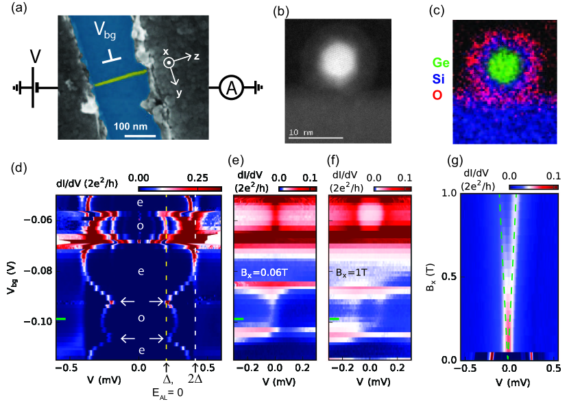
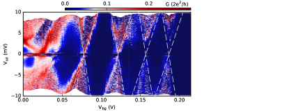
To perform tunneling spectroscopy measurements the bottom gate voltage is used to vary the barriers of the quantum dot and alter the density of the holes as well. From a large source-drain voltage measurement (Supplementary Fig. 1), we estimate a charging energy of 12 meV, barriers’ asymmetry of = 0.2-0.5, where is the coupling to the left (right) lead, and a lever arm of 0.3 eV/V. In Fig. 1d, the differential conductance as a function of a versus reveals a superconducting gap (2 = 380 eV) and several Andreev processes within this window. Additionally, an even-odd structure shows up in both the superconducting state at low and normal state at high , which is related to the even or odd parity of the holes in the quantum dot. The even-odd structure persists as we suppress the superconductivity in the device by applying a small magnetic field (60 mT) perpendicular to the substrate (Fig. 1e). A zero bias peak appears when the quantum dot has odd parity. This is a signature of the Kondo effect 16, 17. When increasing the magnetic field to 1 T, the Kondo peak splits due to the Zeeman effect by . The energy splitting of the two levels is linear as shown in Fig. 1g, and thus can be used to extract a Landé g-factor of 1.9. In the remainder of the letter we will discuss the three magnetic field regimes of Fig. 1d-f (0 T, 60 mT and 1T, respectively) in more detail.
 \justify
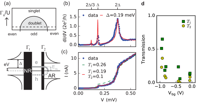
The resonance that disperses with in Fig. 1d is an Andreev Level (AL), which is the energy transition from the ground to the excited state in the dot 18, 19. The ground state of the dot switches between singlet and doublet if the occupation in the dot changes, as sketched in the phase diagram in the top panel of Fig. 2a. Since our charging energy is large, we trace the dashed line in the phase diagram. The AL undergoes Andreev reflection at the side of the quantum dot with large coupling () and normal reflection at the opposite side that has lower coupling (), as schematically drawn in bottom panel of Fig. 2a. The superconducting lead with the low coupling serves as a tunneling spectroscopy probe of the density of states. To be more precise, the coherence peak of the superconducting gap is the probing the Andreev level energy . For example if we measure it at , the resonance thus has an offset of in the measurement in Fig 1d. The ground state transition is visible as a kink of the resonance at = at = -0.09 mV and -0.11 mV. At more negative the coupling of the hole gas to the superconducting reservoirs is strongly enhanced. This eventually leads to the observation of both the DC and AC Josephson effects (Supplementary Fig. 2).
In the upper part of Fig. 1d we measure multiple Andreev reflection (MAR): resonances at integer fractions of the superconducting gap. Fig. 2b presents a line trace at = -0.85 V that shows the gap edge and first- and second- order Andreev reflection. Fitting the differential conductance 20, 21 (see Supplementary) allows us to extract = 190 eV, close to the bulk gap of Al. We also fit the measured current to extract the transmission of the spin degenerate longitudinal modes in the NW (Fig. 2c) 22, 23. The two-mode fit resembles the data better than the single mode fit. Therefore the first provides us an estimate for the transmission in the two modes, and . We interpret the two modes as two semiconducting bands in the NW. The MAR fitting analysis is repeated at different and the resulting and are plotted in Fig. 2d. The strong increase of the transmission below = -0.8 V is attributed to the increase of the Fermi level, and and .
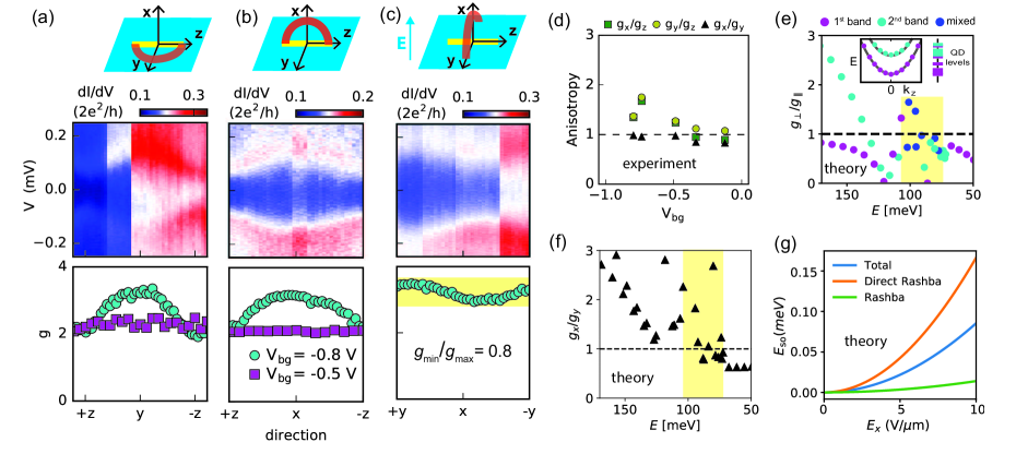
The Landé g-factor is investigated further by measuring the Kondo peak splitting as a 0.9 T magnetic field is rotated from - to -, - to - and - to -direction as presented in the second row of Fig. 3a-c. Interestingly, we find a strong anisotropy of the Kondo peak splitting and accordingly of at = -0.79 V (bottom row Fig. 3a-c). Both directions perpendicular to the NW show a strongly enhanced . Similar anisotropy has been reported before in a closed quantum dot, where is even quenched in the -direction 24, 25, 26. In our experiment the highest of 3.5 is found when the magnetic field is pointed perpendicular to the NW, and almost perpendicular to the substrate.
On the contrary, at a = -0.5 V we find an isotropic (bottom row of Fig. 3a-c), all of which have a value of around 2. The anisotropies at different are summarized in Fig. 3d. The strong anisotropy seems to set in around = -0.7 V. This sudden transition from isotropic to anisotropic , which has not been observed before in a quantum dot system, is correlated with the increase in transmission in Fig. 2d. We speculate that the change from isotropic to anisotropic behaviour is related to the occupation of two bands in the NW. To test this hypothesis and get an understanding of the origin of the anisotropy we theoretically model the band structure of our NW and focus on the two lowest bands.
We use the model described in Ref. 4 and apply it to our experimental geometry (see Supplementary for details). Simulating the device as an infinite wire we first consider the anistropy of between the directions parallel and perpendicular to the NW. We find that there are two contributions to the anisotropy: the Zeeman and the orbital effect of the magnetic field 27, 28. The anisotropy of the Zeeman component is similar for the two lowest bands, where for the orbital part the anisotropy differs strongly. The anisotropy of the total therefore shows a strong difference for the two lowest bands (Supplementary Figs. 5-6). This agrees qualitatively with earlier predictions3, but we find additionally that strain lifts the quenching of along the NW such that , in agreement with our measurements. From these observations we conclude that the observed isotropic and anisotropic with respect to the NW-axis is due to the orbital effect.
In addition, we include the confinement along the NW, such that a quantum dot is formed and the energy levels are quantized in the -direction. Besides the lowest energy states studied before,24, 6 we also consider a large range of higher quantum dot levels. In the regime where two bands are occupied we observe that the quantum dot levels originating from the first and second band have a unique ordering as a function of Fermi energy, this situation is sketched in the inset of Fig. 3e. We also find that some of the quantum dot levels are a mixture of the two bands (Supplementary Fig. 8), resulting in a different anisotropy for each quantum dot level. In the simulation results (Fig. 3e and Supplementary Fig. 9) the anisotropy values are colored according to the band they predominantly originate from. To compare the simulation with the measured data we note that a more negative in the experiment increases the Fermi level for holes . In the simulation we observe a regime in (highlighted in Fig. 3e), where the anisotropy / is around 1 and goes up towards 2 as increases. This behaviour qualitatively resembles the measurement of and in Fig. 3d.
Now we turn to the magnetic field rotation in the -plane, the two directions perpendicular to the NW that are parallel and perpendicular to the electric field induced by the bottom gate. The measured anisotropy is / = 0.8 (Fig. 3c). The maximum of 3.5 is just offset of the -direction, which is almost parallel to the electric field. This anisotropy with respect to the electric field direction is a signature of SOI 24, 25. As discussed before, the Ge-Si NWs are predicted to have both Rashba SOI and direct Rashba SOI 3, 6. The electric field could also cause anisotropy via the orbital effect or geometry, due to an anisotropic wavefunction. However we can rule that out since our simulations show that the wavefunction does not significantly change as electric field is applied (Supplementary Fig. 7). In the simulation (Fig. 3f) with a constant electric field of 10 mV/m, we observe anisotropy of parallel () and perpendicular() to the electric field. Similar to our data the anisotropy starts below 1 and goes to 1 as the Fermi level is increased. The spread in the anisotropy values is due to the mixing of the bands for each quantum dot level. Furthermore we calculated the magnitude of the Rashba and direct contribution to the SOI and find the direct Rashba SOI is dominating in the small diameter nanowires of our study (Fig. 3g). This agrees with the effective Hamiltonian derived in Ref. 3, which predicts that the direct Rashba SOI dominates in NWs with a Ge core of 3 nm radius. To summarize, we observe anisotropy with respect to the electric field direction that is caused by SOI, which is likely for the largest part due to the direct Rashba SOI.
 \justify
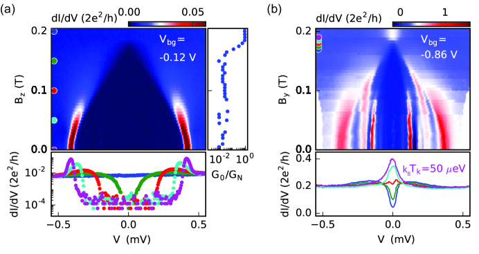
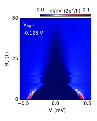
Finally, in Fig. 4 we take a detailed look at the superconducting gap as a function of magnetic field. We find the critical magnetic field for different directions: = 220 mT (Fig. 4a), = 220 mT (Fig. 4b), and = 45 mT(Fig. 1g and Supplementary Fig. 3), consistent with an Al thin film. In the tunneling regime at = -0.12 V, we observe a clean gap closing (Fig. 4a). The conductance inside the gap is suppressed by two orders of magnitude, signaling a low quasiparticle density of states in the superconducting gap. This large conductance suppression remains as the gap size decreases towards (bottom panel in Fig. 4a). In the low conductance regime we thus measure a hard superconducting gap persisting up to in Ge-Si NWs.
The closing of the superconducting gap in a higher conductance regime is presented in Fig. 4b. Since the transmission is increased, Andreev reflection processes cause a significant conductance within the superconducting gap 29. Therefore the conductance suppression in the gap becomes an ill-defined measure of the quasiparticle density of states and with that the quality of the induced superconductivity. However, here we can use the Kondo peak to examine the quasiparticle density of states in the superconducting gap. The Kondo peak is formed by coupling through quasiparticle states within the window of the Kondo energy (). In the regime where , the existence and size of the Kondo peak is then an indication of the quasiparticle density of states inside the superconducting gap 30, 31. In our measurement is indeed than up to a magnetic field = 170 mT (see the blue and magenta line traces in bottom panel of Fig. 4b). Since in the measurement the Kondo peak only arises once the gap is fully closed, we have a low quasiparticle density of states within the superconducting gap. This supports our observation of a hard superconducting gap up to . It also illustrates a new way of gauging whether the superconducting gap is hard in a high conductance regime.
Combining all three magnetic field regimes of Fig. 2-4, we observed: Andreev levels showing a ground state transition; SOI from the coexistence of two bands in Ge-Si core-shell NWs; and a hard superconducting gap. The combination and correlation of these observations is a crucial step for exploring this material system as a candidate for creating a one-dimensional topological superconductor.
0.1 Associated Content
Supporting Information
The supporting information entails extra experimental data and a description and intermediate results of the band structure calculations.
0.2 Author Information
Author contributions
F.K.d.V. and J.S. designed the experiment, fabricated the devices and performed the measurements. M.P.N. and M.W. did the MAR fitting. R.S., D.V., L.W., and M.W. performed band structure calculations. J.R. and F.Z. contributed to the discussions of data. A.L. and E.P.A.M.B. grew the material. S.K., and M.A.V. did TEM analysis. L.P.K. and J.S. supervised the project. F.K.d.V., J.S. and R.S. wrote the manuscript. All authors commented on the manuscript.
Notes
The authors declare no competing financial interests.
0.3 Acknowledgements
The authors thank M. C. Cassidy for fruitful discussions about the fabrication and Y. Ren for help with the growth. This work has been supported by funding from the Netherlands Organisation for Scientific Research (NWO), Microsoft Corporation Station Q and the European Research Council (ERC HELENA 617256 and ERC Starting Grant 638760). We acknowledge Solliance, a solar energy R&D initiative of ECN, TNO, Holst, TU/e, imec and Forschungszentrum Jülich, and the Dutch province of Noord-Brabant for funding the TEM facility. M.P.N. acknowledges support by the National Science Centre, Poland (NCN).
References
- Xiang et al. 2006 Xiang, J.; Lu, W.; Hu, Y.; Wu, Y.; Yan, H.; Lieber, C. M. Ge/Si nanowire heterostructures as high-performance field-effect transistors. Nature 2006, 441, 489 EP –
- Conesa-Boj et al. 2017 Conesa-Boj et al., S. Boosting Hole Mobility in Coherently Strained [110]-Oriented Ge-Si Core-Shell Nanowires. Nano Lett. 2017, 17, 2259–2264
- Kloeffel et al. 2011 Kloeffel, C.; Trif, M.; Loss, D. Strong spin-orbit interaction and helical hole states in Ge/Si nanowires. Phys. Rev. B 2011, 84, 195314
- Kloeffel et al. 2018 Kloeffel, C.; Rančić, M. J.; Loss, D. Direct Rashba spin-orbit interaction in Si and Ge nanowires with different growth directions. Phys. Rev. B 2018, 97, 235422
- Nadj-Perge et al. 2010 Nadj-Perge, S.; Frolov, S. M.; Bakkers, E. P. A. M.; Kouwenhoven, L. P. Spin-orbit qubit in a semiconductor nanowire. Nature 2010, 468, 1084–7
- Kloeffel et al. 2013 Kloeffel, C.; Trif, M.; Stano, P.; Loss, D. Circuit QED with hole-spin qubits in Ge/Si nanowire quantum dots. Phys. Rev. B 2013, 88, 241405
- Alicea 2012 Alicea, J. New directions in the pursuit of Majorana fermions in solid state systems. Rep. Prog. Phys. 2012, 75, 076501
- Maier et al. 2014 Maier, F.; Klinovaja, J.; Loss, D. Majorana fermions in Ge/Si hole nanowires. Phys. Rev. B 2014, 90, 195421
- 9 Mourik et al., V. Signatures of Majorana fermions in hybrid superconductor-semiconductor nanowire devices. Science 336, issue = 6084, pages = 1003-1007, ISSN = 0036-8075, year = 2012, type = Journal Article
- Deng et al. 2016 Deng et al., M. T. Majorana bound state in a coupled quantum-dot hybrid-nanowire system. Science 2016, 354, 1557–1562
- Chang et al. 2015 Chang et al., W. Hard gap in epitaxial semiconductor-superconductor nanowires. Nat Nanotech. 2015, 10, 232–6
- Gul et al. 2017 Gul et al., O. Hard Superconducting Gap in InSb Nanowires. Nano Lett. 2017, 17, 2690–2696
- Xiang et al. 2006 Xiang, J.; Vidan, A.; Tinkham, M.; Westervelt, R. M.; Lieber, C. M. Ge/Si nanowire mesoscopic Josephson junctions. Nature Nanotech. 2006, 1, 208–13
- Su et al. 2016 Su et al., Z. High critical magnetic field superconducting contacts to Ge/Si core/shell nanowires. arXiv preprint arXiv:1610.03010 2016,
- Ridderbos 2018 Ridderbos, J. Quantum dots and superconductivity in Ge-Si nanowires. Dissertation, 2018
- Goldhaber-Gordon et al. 1998 Goldhaber-Gordon et al., D. Kondo effect in a single-electron transistor. Nature 1998, 391, 156
- Cronenwett et al. 1998 Cronenwett, S. M.; Oosterkamp, T. H.; Kouwenhoven, L. P. A Tunable Kondo Effect in Quantum Dots. Science 1998, 281, 540–544
- Deacon et al. 2010 Deacon et al., R. S. Tunneling spectroscopy of Andreev energy levels in a quantum dot coupled to a superconductor. Phys. Rev. Lett. 2010, 104, 076805
- Lee et al. 2014 Lee et al., E. J. Spin-resolved Andreev levels and parity crossings in hybrid superconductor-semiconductor nanostructures. Nature Nanotech. 2014, 9, 79–84
- Averin and Bardas 1995 Averin, D.; Bardas, A. ac Josephson Effect in a Single Quantum Channel. Phys. Rev. Lett. 1995, 75, 1831–1834
- Kjaergaard et al. 2017 Kjaergaard et al., M. Transparent Semiconductor-Superconductor Interface and Induced Gap in an Epitaxial Heterostructure Josephson Junction. Phys. Rev. Applied 2017, 7, 034029
- Scheer et al. 1997 Scheer, E.; Joyez, P.; Esteve, D.; Urbina, C.; Devoret, M. H. Conduction Channel Transmissions of Atomic-Size Aluminum Contacts. Phys. Rev. Lett. 1997, 78, 3535–3538
- Goffman et al. 2017 Goffman et al., M. F. Conduction channels of an InAs-Al nanowire Josephson weak link. New Journal of Physics 2017, 19, 092002
- Maier et al. 2013 Maier, F.; Kloeffel, C.; Loss, D. Tunable gfactor and phonon-mediated hole spin relaxation in Ge/Si nanowire quantum dots. Phys. Rev. B 2013, 87, 161305(R)
- Brauns et al. 2016 Brauns, M.; Ridderbos, J.; Li, A.; Bakkers, E. P. A. M.; Zwanenburg, F. A. Electric-field dependent g-factor anisotropy in Ge-Si core-shell nanowire quantum dots. Phys. Rev. B 2016, 93, 121408(R)
- Brauns et al. 2016 Brauns et al., M. Anisotropic Pauli spin blockade in hole quantum dots. Phys. Rev. B 2016, 94, 041411(R)
- Nijholt and Akhmerov 2016 Nijholt, B.; Akhmerov, A. R. Orbital effect of magnetic field on the Majorana phase diagram. Phys. Rev. B 2016, 93, 235434
- Winkler et al. 2017 Winkler et al., G. W. Orbital Contributions to the Electron Factor in Semiconductor Nanowires. Phys. Rev. Lett. 2017, 119, 037701
- Blonder et al. 1982 Blonder, G. E.; Tinkham, M.; Klapwijk, T. M. Transition from metallic to tunneling regimes in superconducting microconstrictions: Excess current, charge imbalance, and supercurrent conversion. Phys. Rev. B 1982, 25, 4515–4532
- Buitelaar et al. 2002 Buitelaar, M. R.; Nussbaumer, T.; Schonenberger, C. Quantum dot in the Kondo regime coupled to superconductors. Phys. Rev. Lett. 2002, 89, 256801
- Lee et al. 2012 Lee et al., E. J. Zero-bias anomaly in a nanowire quantum dot coupled to superconductors. Phys. Rev. Lett. 2012, 109, 186802
Supplementary Material
Spin-orbit interaction and induced superconductivity in an one-dimensional hole gas
F. K. de Vries, J. Shen, R.J. Skolasinski, M. P. Nowak, D. Varjas, L. Wang, M. Wimmer, J. Ridderbos, F. A. Zwanenburg, A. Li, S. Koelling, M. A. Verheijen, E. P. A. M. Bakkers and L. P. Kouwenhoven
1 Calculation of multiple Andreev reflection and the fitting procedure
The conductance and the current response of the voltage biased nanowire Josephson junction are calculated following the scattering approach introduced by Averin and Bardas in Ref. 2. The model accounts for sequential Andreev reflections of electrons and holes accelerated by the voltage bias that propagate through the normal part of a SNS junction. The total DC current of a multimode junction is obtained 3 as a sum of the currents carried by individual modes of the transverse quantization
| (1) |
where is the transmission probability of the ’th mode and is the superconducting gap.
The transmission probabilities and the superconducting gap of the measured nanowire junction are inferred by fitting the numerically obtained current to the experimental one through minimization of . is a free parameter of the fitting procedure. We have checked that increase of above 2 results in the transmission probabilities evidencing the presence of only two conducting modes in the structure as described in the main text. The analogous procedure is performed for the differential conductance traces, obtained in the numerics by differentiation of the calculated current over the bias voltage.
2 Numerical calculations
2.1 Discussion of previous results and overview
Our experimental data shows a g-factor with a gate-tunable anisotropy. A g-factor anisotropy for Ge-Si core-shell nanowires with a circular crosssection and in the absence of electric fields was predicted for the lowest two subbands in Ref. 4: At , the g-factors for the lowest subband were computed to be and , for the second subband and . Comparing to the experimentally measured values, we observe that (i) the computed anisotropy in the lowest subband is larger than in the second subband, whereas we observe a quenched anisotropy for lower densities, and (ii) the experimentally measured never drops below 2. A later numerical simulation including strain found for the lowest subband and 5, i.e. bringing the g-factor for field parallel to the wire closer to our experimental results. However, no results were given for the second subband there. Ref. 6 discussed the electric field dependence of the g-factor anisotropy for the ground state in a quantum dot in the Ge-Si core-shell nanowire, and found that the anisotropy was quenched with increasing electric field due to the direct Rashba SOI. Again, this is opposite to our experimental observation that the anisotropy is quenched for small (absolute) gate voltages.
We can thus not directly interpret our results in terms of existing theory. For this reason we apply the model described in Ref. 5 to our experimental geometry and strain values. As we show below, strain can change g-factor values up to an order of magnitude and even reverse anisotropies. We also find that we need to consider excited quantum dot states to find agreement with the experimental data.
2.2 Model for nanowire along [110]
We use the Luttinger-Kohn Hamiltonian for holes that has been established for modelling Ge-Si core shell nanowires 4, 5. Below we give this Hamiltonian in detail, the description was adapted from Ref. 5. The bulk Hamiltonian of the Ge core is
| (2) |
where is the Luttinger-Kohn (LK) Hamiltonian, the coupling to the electric field that is known to give rise to the direct Rashba spin-orbit interaction (SOI) 4, is the indirect Rashba SOI due to coupling to other bands, and is the Bir-Pikus Hamiltonian describing the effects of strain. The magnetic field is included through the Zeeman term , and the orbital effect. We consider the orbital effect of the field through kinetic momentum substitution. We include a global “” sign in our Hamiltonian such that hole states have a positive effective mass. In the following we take a detailed look at each term in the Hamiltonian separately.
Luttinger-Kohn Hamiltonian
| (3) |
where are the Luttinger parameters, is the electron mass, are the spin- matrices, , “c.p.” stands for cyclic permutation, and is the anticommutator.
Magnetic field
We include magnetic field through the Zeeman term 8, 9
| (4) |
and the orbital effect by the following substitution in the Hamiltonian
| (5) |
where , the vector potential, is the flux quantum with being positive elementary charge and the Planck constant. The anisotropic Zeeman term 9, 8, where , is omitted as for Si and Ge 5, 10.
Electric field
Strain effect
In our numerical calculations we only simulate the Ge core, and include the presence of the Si shell through the strain that it induces in the core 4. We model the strain using the Bir-Pikus Hamiltonian 11
| (8) |
where are the deformation potentials and are the strain tensor elements. Similarly to the Luttinger-Kohn Hamiltonian the spherical approximation can be used and strain may assumed to be constant in the Ge core 12. Thus, , , and . The Bir-Pikus Hamiltonian then simplifies to the spherical symmetric form 12
| (9) |
where a global energy shift has been omitted.
2.2.1 Material parameters
2.2.2 Numerical method
We perform our numerical calculations using Kwant 14. We use the finite difference method to discretize the Hamiltonian (2) on a cubic grid with spacing . Depending on the geometry we use two slightly different methods.
The first approach is suitable for simulating a translation invariant infinite wire system, by considering the Hamiltonian
| (10) |
The transverse momenta and are treated as differential operators, which are discretized as finite difference operators. The Hamiltonian is then represented in a tight-binding form, and a finite system in the -plane is generated that represents the wire cross section. The cross section has either a square or hexagon shape. The momentum along the wire, , remains a scalar parameter.
In the second approach we treat all momenta as differential operators:
| (11) |
In addition to a finite cross section in the -plane we terminate the wire in the -direction, effectively obtaining a quantum dot of length .
The Landé -factors are extracted from the energy spectrum of the system as a split in energies caused by the finite magnetic field
| (12) |
where is band number, is Bohr magneton, and is the magnitude of the magnetic field. For the infinite wire we use the energy split at . We note that this numerical approach goes beyond the effective Hamiltonian approach in Ref. 4 and also takes into account the effects of higher states. The accuracy of our approach is controlled by the grid spacing .
2.2.3 Model geometry and verification
The nanowires used in our experiment have a hexagonal cross-section with a corner-to-corner width of nm. Faithfully representing this shape with a cubic lattice requires a rather small lattice spacing that is computationally unfavorable.
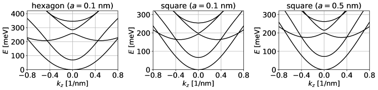
Figure S4 shows the comparison of the band structure between the wires with hexagon (left) and square (middle) shaped cross sections calculated using the grid spacing nm. We observe that the impact of the cross section shape on the qualitative result is small, in agreement with what was reported for the comparison between a circular and square cross section5. Hence we use a square cross section with nm side length in further calculations.
This choice allows us to use a larger grid spacing ( nm) that significantly reduces the computational cost of the calculation. For grid spacing nm the square cross section preserves the symmetries of the system and key features of the dispersion of two lowest subbands, see middle and right panel on Fig. S4. We also note that the band structures we observe agree qualitatively with what was reported earlier 4, 5, further verifying the accuracy of our approach.
2.3 Simulation code and dataset
All simulation codes used in this project are available under (simplified) BSD licence together with raw simulation data 15.
2.4 Results
2.4.1 Infinite wire
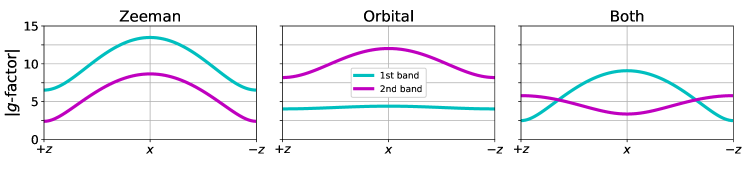
We first investigate the infinite wire system. In Fig. S5 we present the anisotropy of the -factors when a magnetic field is included only through the Zeeman term, only the orbital effect, and both of these contributions, respectively. The direction of magnetic field changes from along the axis (parallel to the wire) to the axis (antiparallel to the wire). No electric field is present in the system. The results show that the states behave differently in the lowest two subbands. In the lowest state the anisotropy originates almost exclusively from the Zeeman term. On the other hand, in the second state the Zeeman and orbital contributions both have significant anisotropies but opposite signs, such that they partially cancel (note that the graphs show absolute values of the -factors). Comparing to Ref. 4 we find increased g-factor values, such as an order-of-magnitude enhancement of in the lowest suband. We can attribute this to strain, as our numerical simulations yield g-factor values comparable to Ref. 4 in the absence of strain. Also, strain leads to in the second subband, reversing the anisotropy. Note also that our results for the lowest subband agree better with the results of Ref. 5 with a somewhat weaker strain than in our situation.
In Fig. S6 we analyse the anisotropy as the magnetic field orientation changes with respect to the wire from the parallel to antiparallel direction (left and middle) and around the perpendicular directions (right), in the absence and presence of electric fields. The magnetic field is rotated from to axis through (left) and (middle). In the right panel magnetic field changes from through to . The upper row corresponds to systems with no electric field whereas the bottom row corresponds to systems with perpendicular electric field that we estimate for our experimental situation. Due to the fourfold rotational symmetry, -factors are identical for and directions in the abscence of electric field as expected. This symmetry is in principle broken by the applied field, but the anisotropy between and remains small for experimentally relevant field strengths.
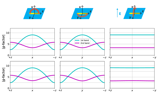
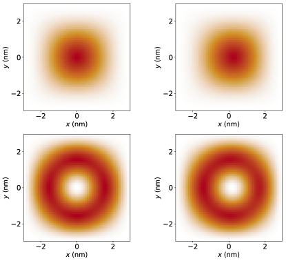
Indeed, we observe that due to the large confinement energy (around 80meV, see Fig. S4) the effect of the electric field on the states in the infinite wire is almost negligible, as demonstrated in Fig. S7 (note that the shape of these wave functions in the absence of electric fields is in agreement with previous results 16, 4, 5).
In summary, we find that the g-factor anisotropy of the lowest subbands is modified considerably by strain. However, the results also do not agree with our experimental finding of a quenched anisotropy at lower densities. For this reason, we now turn to quantum dots.
2.5 Quantum dot
As explained in the main text, the experiment accesses higher states of the quantum dot, which originate from different subbands. In this section we show results for a quantum dot of length nm (with hard-wall boundary conditions), corresponding to the experimental setup. The discretization grid has nm.
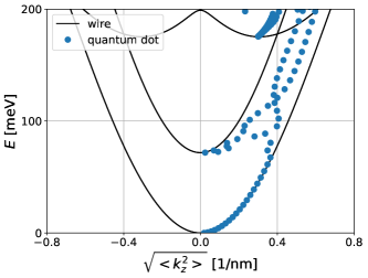
Fig. S8 shows the energy levels in the quantum dot as a function of evaluated in the given eigenstate. The states near the bottom of the lowest subband trace the infinite wire’s dispersion very accurately, confirming the particle-in-box momentum quantization picture. When the second subband enters, the quantum dot levels significantly deviate from the infinite wire dispersion. This is a finite size effect, the result of mixing between states from different subbands with different (note that in a finite wire is not a conserved quantity). For most of the energy window with two subbands the two branches of the dispersion are clearly distinguishable, supporting the view that consecutive quantum dot states inherit properties from different subbands.
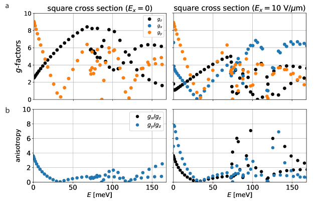
Fig. S9a and Fig. S9b show the -factors and -factor anisotropies in the finite quantum dot respectively. At low energies, Fig. S9a reveals in the absence of an electric field () and in the presence of . This is in qualitative agreement with previous calculations for the ground states in Ge-Si NW quantum dots 6. Also, at finite has recently been observed experimentally 17. Where the second subband enters, the -factor values split into two branches corresponding to the first and second subbands, this is especially visible in the values. The external electric field induces a much larger anisotropy between and in higher states compared to the lowest one accessed at , that was discussed previously in Ref. 6. Since the effect of the electric field on the g-factor in the infinite wire case is small, we attribute the increased anisotropy to spin-momentum locking present at nonzero .
References
- Ridderbos 2018 Ridderbos, J. Quantum dots and superconductivity in Ge-Si nanowires. Dissertation, 2018
- Averin and Bardas 1995 Averin, D.; Bardas, A. ac Josephson Effect in a Single Quantum Channel. Phys. Rev. Lett. 1995, 75, 1831–1834
- Bardas and Averin 1997 Bardas, A.; Averin, D. V. Electron transport in mesoscopic disordered superconductor normal-metal superconductor junctions. Phys. Rev. B 1997, 56, R8518–R8521
- Kloeffel et al. 2011 Kloeffel, C.; Trif, M.; Loss, D. Strong Spin-Orbit Interaction and Helical Hole States in Ge/Si Nanowires. Phys. Rev. B 2011, 84, 195314
- Kloeffel et al. 2018 Kloeffel, C.; Rančić, M. J.; Loss, D. Direct Rashba spin-orbit interaction in Si and Ge nanowires with different growth directions. Phys. Rev. B 2018, 97, 235422
- Maier et al. 2013 Maier, F.; Kloeffel, C.; Loss, D. Tunable gfactor and phonon-mediated hole spin relaxation in Ge/Si nanowire quantum dots. Phys. Rev. B 2013, 87, 161305(R)
- Luttinger and Kohn 1955 Luttinger, J. M.; Kohn, W. Motion of Electrons and Holes in Perturbed Periodic Fields. Phys Rev 1955, 97, 869–883
- Luttinger 1956 Luttinger, J. M. Quantum Theory of Cyclotron Resonance in Semiconductors: General Theory. Phys. Rev. 1956, 102, 1030–1041
- Winkler 2003 Winkler, R. Spin-Orbit Coupling Effects in Two-Dimensional Electron and Hole Systems; Springer: Berlin, Heidelberg, 2003
- Lawaetz 1971 Lawaetz, P. Valence-Band Parameters in Cubic Semiconductors. Phys Rev B 1971, 4, 3460–3467
- Bir and Pikus 1974 Bir, G. L.; Pikus, G. Symmetry and strain-induced effects in semiconductors; 1974
- Kloeffel et al. 2014 Kloeffel, C.; Trif, M.; Loss, D. Acoustic Phonons and Strain in Core/Shell Nanowires. Phys. Rev. B 2014, 90
- Conesa-Boj et al. 2017 Conesa-Boj, S.; Li, A.; Koelling, S.; Brauns, M.; Ridderbos, J.; Nguyen, T. T.; Verheijen, M. A.; Koenraad, P. M.; Zwanenburg, F. A.; Bakkers, E. P. A. M. Boosting Hole Mobility in Coherently Strained [110]-Oriented Ge-Si Core-Shell Nanowires. Nano Lett. 2017, 17, 2259–2264
- Groth et al. 2014 Groth, C. W.; Wimmer, M.; Akhmerov, A. R.; Waintal, X. Kwant: a software package for quantum transport. New J. Phys. 2014, 16, 063065
- de Vries et al. 2018 de Vries, F. K.; Shen, J.; Skolasinski, R.; Nowak, M. P.; Varjas, D.; Wang, L.; Wimmer, M.; Ridderbos, J.; Zwanenburg, F.; Li, A.; Verheijen, M. A.; Bakkers, E. P. A. M.; Kouwenhoven, L. P. Simulation codes and data for Spin-orbit interaction and induced superconductivity in an one-dimensional hole gas. 2018; \urlhttps://doi.org/10.5281/zenodo.1310873
- Csontos and Zülicke 2007 Csontos, D.; Zülicke, U. Large variations in the hole spin splitting of quantum-wire subband edges. Phys. Rev. B 2007, 76, 073313
- Brauns et al. 2016 Brauns, M.; Ridderbos, J.; Li, A.; Bakkers, E. P. A. M.; Zwanenburg, F. A. Electric-field dependent g-factor anisotropy in Ge-Si core-shell nanowire quantum dots. Phys. Rev. B 2016, 93, 121408(R)