Mapping of Lattice Surgery-based Quantum Circuits on Surface Code Architectures
Abstract.
Quantum error correction (QEC) and fault-tolerant (FT) mechanisms are essential for reliable quantum computing. However, QEC considerably increases the computation size up to four orders of magnitude. Moreover, FT implementation has specific requirements on qubit layouts, causing both resource and time overhead. Reducing spatial-temporal costs becomes critical since it is beneficial to decrease the failure rate of quantum computation. To this purpose, scalable qubit plane architectures and efficient mapping passes including placement and routing of qubits as well as scheduling of operations are needed. This paper proposes a full mapping process to execute lattice surgery-based quantum circuits on two surface code architectures, namely a checkerboard and a tile-based one. We show that the checkerboard architecture is x qubit-efficient but the tile-based one requires lower communication overhead in terms of both operation overhead (up to ) and latency overhead (up to ).
1. Introduction
By exploiting superposition and entanglement, quantum computing can outperform classical computing while solving certain problems. For example, quantum computers can factor large numbers using Shor’s algorithm with an exponential speedup over its best classical counterparts (shor1994algorithms, ). When adopting the circuit model as a computational model, algorithms can be described by quantum circuits consisting of qubits and gates. Such a circuit representation is hardware agnostic and assumes, for instance, that any arbitrary interaction between qubits is possible and both qubits and gates are reliable.
However, real quantum processors have specific constraints that must be complied to when executing a quantum algorithm, a procedure for mapping quantum circuits is therefore required. One of the main constraints in current quantum experimental platforms is the limited connectivity between qubits. A promising qubit structure that is being pursued for many quantum technologies like superconductors (barends2014superconducting, ; versluis2016scalable, ) and quantum dots (hill2015surface, ; li2017crossbar, ), is a 2D grid architecture that only allows nearest-neighbour (NN) interactions. Other 2D qubit structures such as the quantum processors from IBM (IBM17, ), Google (boixo2016characterizing, ), and Rigetti (sete2016functional, ) have even more restrictive connectivity constraints. This means that non-neighbouring or non-connected qubits need to be moved or routed to be adjacent for interacting -i.e. performing a two-qubit gate, resulting in an overhead in the number of operations as well as the execution time (latency) of the circuit.
Placing frequently interacting qubits close to each other combined with efficient routing techniques -e.g. shortest path- can help to reduce the movement overhead. In addition, exploiting available parallelism of operations will reduce the overall execution time of the circuit. Note that reducing the number of operations and the total circuit latency will be of benefit to decrease the failure rate of computation (bishop2017quantum, ; linke2017experimental, ). Therefore, efficiently mapping quantum circuits on a specific qubit structure, including placement and routing of qubits and scheduling of operations, is necessary for reliable quantum computation. Many works have been done to map physical quantum circuits on different qubit structures. (metodi2006scheduling, ; whitney2007automated, ; dousti12min, ; yazdani2013quantum, ; bahreini2015minlp, ; lye2015determining, ; wille2016look, ; farghadan2017quantum, ) propose algorithms to map physical circuits on quantum processors with 2D NN structures. (IBMQISKIT, ; Zulehner2017efficient, ; siraichi2018qubit, ) and (venturelli2018compiling, ) respectively focus on IBM and Rigetti processors which both only support interactions on dedicated neighbours.
Moreover, quantum hardware is error prone, that is, the qubits loose their states (or decohere) extremely fast and quantum operations are faulty. For instance, superconducting qubits decohere in tens of microseconds (riste2015detecting, ) and quantum operations have error rates (kelly2015state, ) compared to for CMOS based devices. Therefore, quantum error correction (QEC) and fault-tolerant (FT) mechanisms are needed to protect quantum states from errors and make quantum computing FT. This is achieved by encoding a logical qubit into multiple error prone physical qubits and applying FT (logical) operations on such logical qubits (nielsen2010quantum, ). However, QEC significantly increases the computation size up to four orders of magnitude. Furthermore, this FT implementation may lead to more and/or different constraints on the encoded logical circuits, e.g., interaction restrictions between two logical qubits. Consequently, the mapping of fault-tolerant quantum circuits may become more difficult because it should consider both physical-level and logical-level constraints. In addition, it may require the definition of a virtual layer called qubit plane architecture to provide scalable management of qubits and support fast execution of fault-tolerant operations.
Several papers (balensiefer2005quale, ; dousti2013leqa, ; dousti2014squash, ; ahsan2015architecture, ; heckey2015compiler, ; lin2015paqcs, ) have discussed how to map FT quantum circuits onto 2D quantum architectures based on concatenated codes such as Steane code. However, not many papers focus on surface code (SC) (bravyi1998quantum, ), currently one of the most promising QEC codes. (paler2016synthesis, ; paler2017fault, ; paler2017online, ) optimize quantum circuits based on defect surface codes in terms of geometrical volume defined by the product of # qubits and # gates (or time) of the circuit. (javadi2017optimized, ) evaluates both planar and defect surface codes in terms of qubit resources and circuit latency. However, they assume two-qubit gates (CNOT) between two planar qubits can be performed transversally, which is an over-optimistic assumption given the limited connectivity in current quantum technologies. Fortunately, a technique called lattice surgery (horsman2012surface, ; landahl2014quantum, ) can be used to perform a two-qubit gate between two planar qubits in a 2D NN architecture. Nevertheless, the mapping of quantum circuits based on lattice surgery and the required qubit plane architecture have been hardly researched. (horsman2012surface, ) introduces a scalable qubit architecture for efficiently supporting lattice surgery-based two-qubit gates. (herr2017optimization, ) proves that the optimization of lattice surgery-based quantum circuits on its geometrical volume is NP-hard.
This paper will focus on the mapping of lattice surgery-based quantum circuits onto surface code qubit architectures. The contributions of this paper are the following:
-
•
We derive the logical-level constraints of the mapping process when the lattice surgery is used to perform FT operations on planar surface codes. We further provide the quantification of these logical operations, which are used for the mapping passes.
-
•
Based on the qubit plane architecture presented in (horsman2012surface, ), we propose two different qubit architectures, namely a checkerboard architecture and a tile-based one, that support lattice surgery-based operations. For the tile-based architecture, we present an approach to fault-tolerantly swap tiles by lattice surgery, which is x faster than a standard SWAP operation by consecutive logical CNOT gates. In addition, we also apply similar techniques to perform a FT CNOT gate between tiles where logical data qubits are not located in the required positions.
-
•
We propose a full mapping procedure, including placement and routing of qubits and scheduling of operations, to map FT quantum circuits onto the two presented qubit architectures and evaluate these architectures on their communication overhead.
The paper is organized as follows. Section 2 introduces the basics of FT quantum computing. We introduce two qubit plane architectures of interest in Section 3 followed by the proposed mapping passes in Section 4. The evaluation metrics and benchmarks are shown in Section 5. The experimental results are discussed in Section 6. Section 7 concludes.
2. FT quantum computing
Like in classical computing, quantum computing is also built on a two-level system named qubit. A qubit however can be in a superposition of states and : where and are complex numbers. Quantum states can be transformed by performing quantum operations on them. Commonly-used quantum gates include single-qubit gates, such as Pauli-, -, -, Hadamard (), and , and two-qubit gates, such as the Controlled-NOT (CNOT) and SWAP. In a CNOT gate, the target qubit ‘T’ is flipped only if the control qubit ‘C’ is . A SWAP gate interchanges the states of two qubits and can be implemented by three consecutive CNOT gates. The gate set is one of the most popular universal sets of quantum gates, meaning that any arbitrary quantum gate can be approximated within a particular precision by a finite sequence of those gates. Any quantum algorithm can be described by a quantum circuit which consist of qubits and quantum gates.
2.1. Quantum error correction
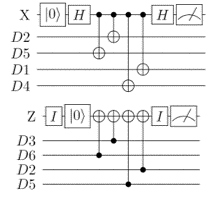
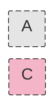
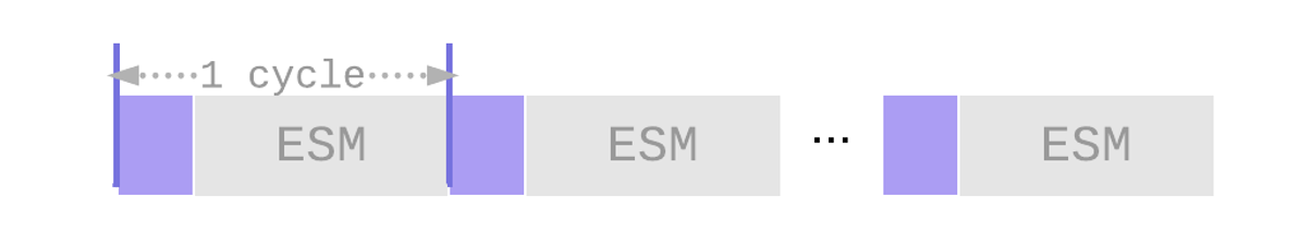
As mentioned before, quantum systems are error prone so that QEC is required for reliable computation. The idea of QEC is to encode a logical qubit into many physical qubits and constantly check the system to detect possible errors. The number of errors that can be corrected is determined by the code distance which is defined as the minimum number of physical operations required to perform a logical operation. Surface code is one of the most promising QEC codes because of its high tolerance to errors (around ) and its simple 2D structure with only NN interactions as shown in Figure 1. It consists of two types of qubits, data qubits (solid circles) for storing computational information, and - or -ancilla qubits (open circles) used to perform stabilizer measurement. The stabilizer measurements are also called error syndrome measurements (ESM) of which circuit description is shown in Figure 1. Note that the CNOT gates are only performed between ancilla qubits and their nearest-neighbouring data qubits. We define a SC cycle as the interval between the starting points of two consecutive ESM.
In surface code, there are two main ways of encoding a single logical qubit, using a planar (dennis2002topological, ) or a defect approach (raussendorf2006fault, ). In planar SC, a single lattice is used to encode one logical qubit. In defect SC, a logical qubit is realized by creating defects in a lattice. For both codes, an implementable universal set of FT logical operations are initialization (Init) and measurement (MSMT) of qubits, Pauli, , , and CNOT gates. However, planar SC requires less physical qubits to encode one logical qubit for the same code distance. In the near-term implementation of quantum computing, qubits are scarce resources and current quantum technologies are pursuing a realization of planar SC quantum hardware (versluis2016scalable, ). This paper therefore focuses on planar surface code. Note that the FT implementation of defect SC (fowler2012surface, ; raussendorf2006fault, ; raussendorf2007fault, ; raussendorf2007topological, ) differs from planar SC, leading to different implications on the mapping procedure.
[width=1.5in]figure/cnot_layout
[width=0.71in]figure/merge
[width=0.89in]figure/split
2.2. Fault-tolerant mechanisms
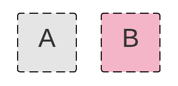
Figure 2 shows three logical qubits based on distance- planar SC and they are labeled as ‘A’, ‘T’ and ‘C’, respectively. Each logical qubit consists of physical qubits and has two types of boundaries, -boundaries and -boundaries. For instance, in lattice ‘A’, the left and right boundaries are -type and the top and bottom boundaries are -type. In planar SC, initialization, measurement, Pauli gates, and can be implemented transversally, i.e., applying bitwise physical operations on a subset of the data qubits, and then performing ESM to detect errors. The FT implementation of and gates in surface code requires ancillary qubits prepared in specific states called magic states. However, the preparation of magic states is not fault-tolerant and produces states with low fidelity that need to be purified by a non-deterministic procedure called state distillation (bravyi2005universal, ; bravyi2012magic, ; meier2012magic, ; jones2013multilevel, ; campbell2017unifying, ). This distillation procedure is repeated until the measurement results indicate one state is successfully purified. On top of that, multiple rounds of successful distillation may be required to achieve the desired state fidelity. Therefore, magic state distillation is the most resource- and time-consuming process in FT quantum computing. Since the and gates can be performed only if their corresponding magic states have been delivered, an online or dynamic scheduling and run-time routing may be required for efficient circuit execution (paler2017online, ). In this paper, we assume magic states have been prepared and properly allocated whenever and gates need to be performed. We will investigate the dynamics of magic state preparation in future work.
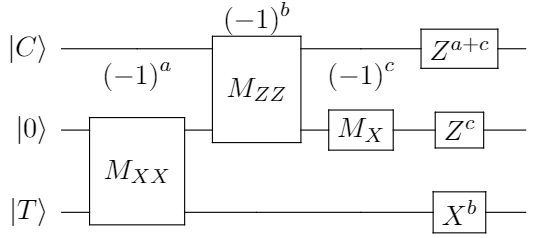
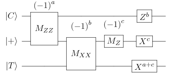
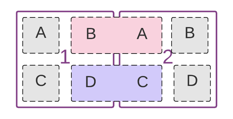
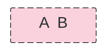
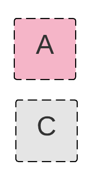
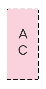
In principle, a FT logical CNOT gate between two planar logical qubits can be performed transversally, i.e., applying pairwise physical CNOT gates to the data qubits in the two lattices. However, this transversal CNOT cannot be realized in current quantum technologies which only allow NN interactions in 2D architectures. Alternatively, a measurement-based procedure (gottesman1998fault, ) which is equivalent to a CNOT gate can be applied and its circuit representations are shown in Figure 3. The joint measurement () is realized by first merging two logical qubits and then splitting them, where their adjacent boundaries are -(-)type boundaries. The outcomes of these measurements will determine whether the corresponding Pauli corrections should be applied (see Appendix A for more details).
The qubit layout for performing the measurement-based CNOT gate in the 2D NN architecture is shown in Figure 2. The realization of the circuit in Figure 3 is achieved as follows: 1) lattices ‘A’ and ‘C’ are merged and then split; 2) lattices ‘A’ and ‘T’ are merged and then split; and 3) measure ‘A’. The merge and split operations are implemented by a technique called lattice surgery (horsman2012surface, ; landahl2014quantum, ). For instance, the merge and split of lattice ‘A’ and ‘C’ are implemented by performing ESM on the integrated lattice (Figure 2) and on the separated lattices (Figure 2), respectively. In general, a surgery-based CNOT takes SC cycles. It is worthy to mention that a split operation between qubits ‘’ and ‘’(‘’) can happen simultaneously with a merge operation between qubits ‘’ and ‘’(‘’). Furthermore, a split operation between two qubits and a measurement on one of them can be performed in parallel. By exploiting the parallelism, the execution time in SC cycles can be reduced to .
2.3. Implications on the mapping problem
Based on the FT implementation of logical operations on planar SC, we derive the following constraints that must be taken into account by the mapping process as well as its implications.
Constraints: 1) The physical 2D NN interaction constraint is intrinsically satisfied by the construction of surface codes, thus the physical-level mapping becomes trivial; 2) A surgery-based CNOT gate requires that the qubits ‘C’ and ‘T’ together with the ancilla qubit ‘A’ are placed in particular neighbouring positions, forming a 90-degree elbow-shaped layout.
Implications: 1) Logical qubits that need to interact and are not placed in such neighbouring positions need to be moved, for instance by means of SWAP operations. The movement of qubits introduces overhead in terms of both qubit resources and execution time; 2) Therefore, in lattice surgery-based SC quantum computing, it is essential to pre-define a qubit plane architecture for efficiently managing qubit resources and supporting communication between logical qubits; 3) In addition, operations for moving qubits should be defined; 4) It is necessary to initially place highly interacting logical qubits as close as possible and apply routing techniques to find the communication paths.
Based on the above observations, we will introduce two slightly different plane architectures and mapping passes for efficient execution of lattice surgery-based quantum circuits in the following sections.
3. Qubit plane architecture
A qubit plane architecture is a virtual layer that organizes the qubits in different specialized and pre-defined areas such as communication, computation and storage (dousti2014squash, ; heckey2015compiler, ). Qubit architectures should be able to manage qubit resources efficiently and provide fast execution of any quantum circuit.
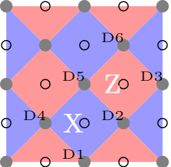
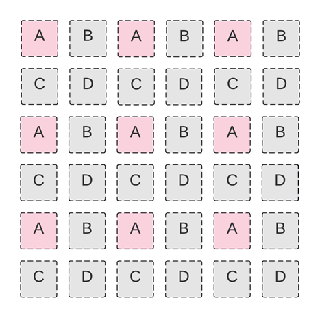
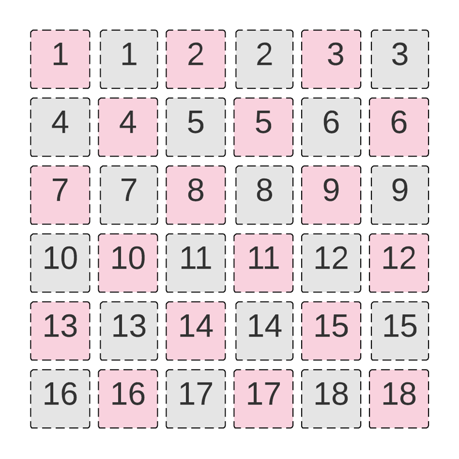
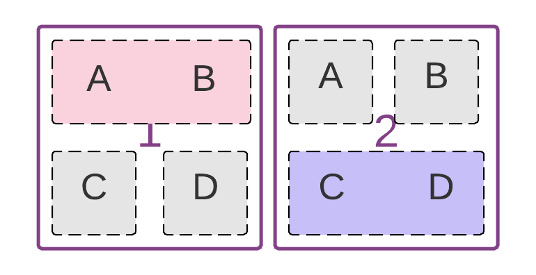
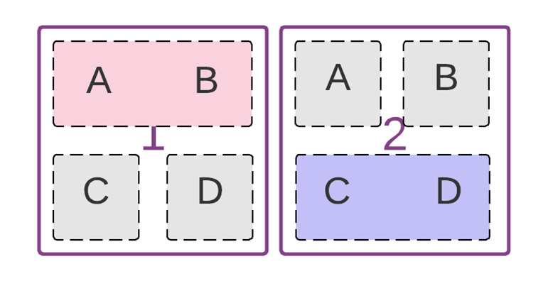
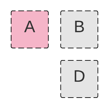
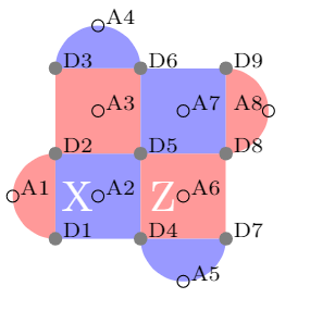
In (horsman2012surface, ), a layout that supports lattice surgery-based CNOT gates on planar SC is presented. As shown in Figure 4, it consists of several patches. The gray patches of the lattice are used for allowing qubits to perform CNOT operations, whereas the pink patches are used for holding logical data qubits. Then, only of the available patches contains logical data qubits. Based on this layout, we propose two slightly different qubit plane architectures, the tile-based architecture (t-arch) and the checkerboard architecture (c-arch) as shown in Figure 5. The pink and purple patches are where logical data qubits containing information can be allocated (data patches), whereas the gray patches are assisting logical qubits (ancilla patches) that are used for performing logical CNOT gates and for communication. These two architectures differ in: i) the number of logical data qubits that can allocate, ii) the way movement operations are implemented, iii) the steps required for performing a CNOT between neighbouring logical data qubits, and iv) the number of neighbours.
Logical data qubit allocation: In the checkerboard architecture, logical data qubits can be assigned to any of the pink patches, that is, of the total patches are used to hold data qubits. In the tile-based architecture, a lined area consisting of logical patches is defined as a basic computation tile and at most one logical data qubit can be allocated in each tile, that is, in either the pink or the purple patch. Then, only of the total number of patches can be used for allocating logical data qubits.
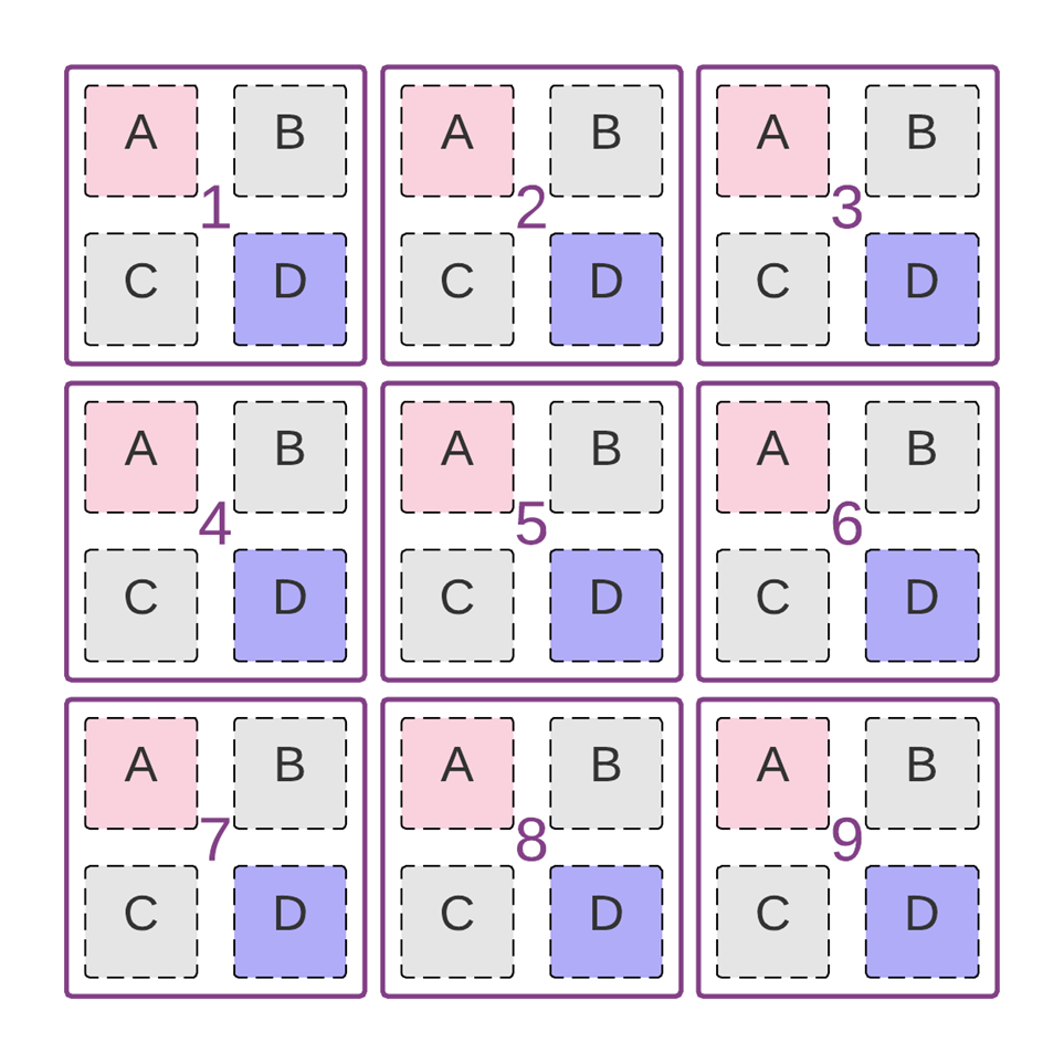
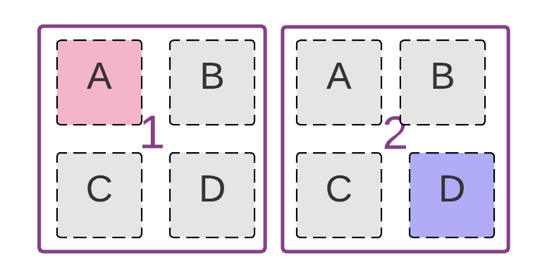
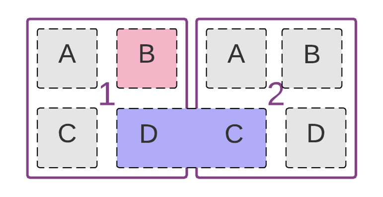
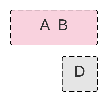
Movement operations: One typical way to move physical qubits is through SWAP operations in which the state of the qubits is exchanged. Usually, a SWAP gate is implemented by applying consecutive CNOT gates. The same principle can be applied for moving logical qubits. In this case a logical SWAP is realized by performing consecutive lattice surgery-based CNOT gates, which is extremely time-consuming ( SC cycles). In the checkerboard architecture, we will use such a swap method called c-SWAP for moving logical qubits because of the limited number of ancilla patches. In the tile-based architecture, we propose to use a faster movement operation, which is analogous to the measurement-based procedure for CNOT gates, to swap data information between two horizontally or vertically adjacent tiles. This swap operation called t-SWAP only takes x logical CNOT gate time regardless of locations where data qubits are allocated inside the tiles -i.e. purple or pink patches. It is realized by ’moving’ qubits to neighbouring horizontal and vertical patches (see Appendix B). Figure 6 shows an example of how to swap two logical data qubits placed in adjacent tiles by using the t-SWAP operation. Similarly, one can perform a t-SWAP between any other pair of patches in the horizontally or vertically adjacent tiles.
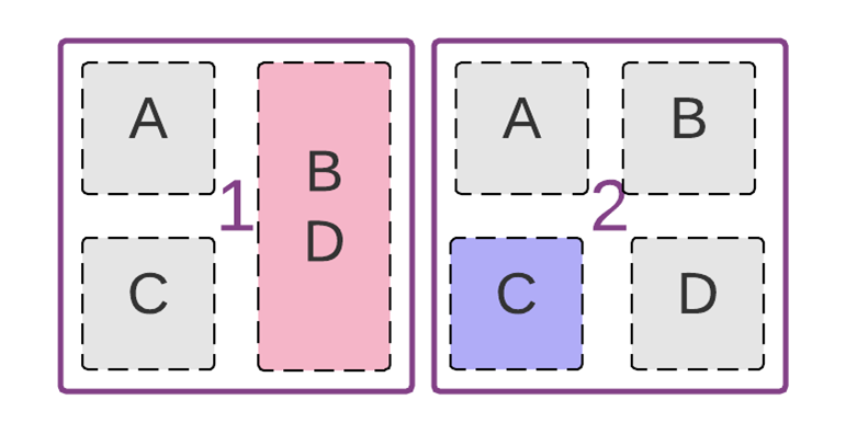
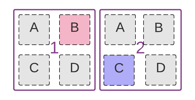
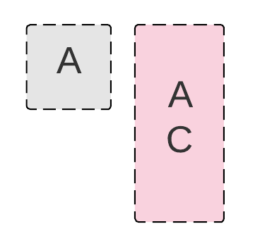
CNOT operations: As mentioned in Section 2, the control and target qubits need to be placed in patches that form a 90-degree elbow-shaped in order to perform a lattice surgery-based CNOT. In the checkerboard architecture, two neighbouring data patches are always in such 90-degree locations so that a lattice surgery-based CNOT gate can be directly performed between them. We called this operation c-CNOT and it is implemented by 3 steps, taking SC cycles as described in the previous section. However, in the tile-based architecture, a CNOT operation called t-CNOT between two data qubits placed in horizontally, vertically, or diagonally adjacent tiles may need some pre-processing, depending on where data qubits are allocated. If the control and target logical qubits are already placed in patches forming a 90-degree shape, then one can perform the CNOT directly, e.g., patch D1 with patches A4, A2, A5. Otherwise, logical data qubits need to be moved to the required locations before performing the CNOT gate as shown in Figure 7.
Similarly, one can perform a t-CNOT between any other pair of patches in adjacent tiles. The t-CNOT with and without pre-processing takes and SC cycles, respectively. In the results section, we will assume that a t-CNOT always takes 4d SC cycles for simplicity.
Number of neighbours: In the checkerboard architecture one data patch can only interact with adjacent data patches, e.g., the neighbours of patch are in Figure 5. As mentioned in Section 2, a logical ancilla is required for performing a lattice surgery-based CNOT gate. To avoid ancilla conflicts when performing multiple logical CNOT gates simultaneously in the checkerboard, only the upper ancilla patch adjacent to the two interacting data patches can be used. For instance, ancilla () will be used when performing a CNOT between data qubits and ( and ). In the tile-based architecture, one tile can interact with at most neighbours, e.g., the neighbours of tile are . However, logical CNOT gates between data qubits in tiles and , and between data qubits in tiles and cannot be performed simultaneously because of ancilla conflicts. To avoid such conflicts for now, we only assume 6 neighbours per tile; we remove the right-top and left-bottom neighbours of each tile, e.g., remove tiles and from the neighbour list of tile .
In the next section, we will introduce the procedure for mapping lattice surgery-based quantum circuits onto both qubit architectures. We will then evaluate their communication overhead in terms of both operation overhead and latency overhead in Section 6 .
4. Quantum circuit mapping
The mapping of quantum circuits involves initial placement and routing of qubits and scheduling of operations. The need for QEC significantly enlarges the circuit size, which makes the mapping problem even more complex. For instance, in surface codes one logical qubit is encoded into physical qubits and one logical operation is implemented by physical operations, where is the code distance. Therefore, we propose to perform the mapping of quantum circuits before going to the physical implementation of logical qubits and operations. It means that each logical qubit is treated as one single unit, and each logical operation is regarded as one single instruction. Once the mapping is finished, logical operations need to be expanded into the corresponding physical operations. We use a library to translate each logical operation into pre-scheduled physical quantum operations (see Appendix C). During the translation, the address of underlying physical qubits corresponding to a logical qubit can be retrieved by maintaining a q-symbol table (fu2016heterogeneous, ).
Table 1 depicts the execution time of different logical operations on planar surface codes expressed in SC cycles. It includes single-qubit operations as well as the two-qubit operations used in both qubit architectures presented previously. The execution time of different operations is used in the scheduling and routing passes. Furthermore, we will use these numbers for calculating the overall circuit latency in Section 5.
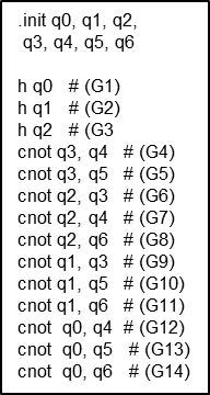
In order to illustrate the different steps in the mapping of quantum circuits, we will use the circuit in Figure 8 described by a quantum assembly language (QASM). This is the encoding circuit of the -qubit Steane code and it can also be used to distill the magic states for gates (fowler2012surface, ). In this case, we assume each qubit is a logical qubit encoded by a distance- planar SC and each operation is a FT operation implemented by the techniques in Section 2 and Section 3.
| Init & MSMT | Pauli | ||||
| # Cycles | |||||
| c-CNOT | c-SWAP | t-CNOT | t-SWAP | ||
| # Cycles |
4.1. Scheduling operations
The objective of the scheduling problem is to minimize the total execution time (circuit latency) of quantum algorithms meanwhile keeping the correctness of the program semantics. Similar to instruction scheduling in classical processors, the correctness can be achieved by respecting the data dependency (hennessy2011computer, ) between quantum operations. Analogous to classical computing, two kinds of data dependency can be defined for quantum computing: true dependency, which is the dependency between two single-qubit gates and between a single-qubit gate and a CNOT gate, and name dependency, which is the dependency between two CNOT gates which have the same control (or target) qubit.
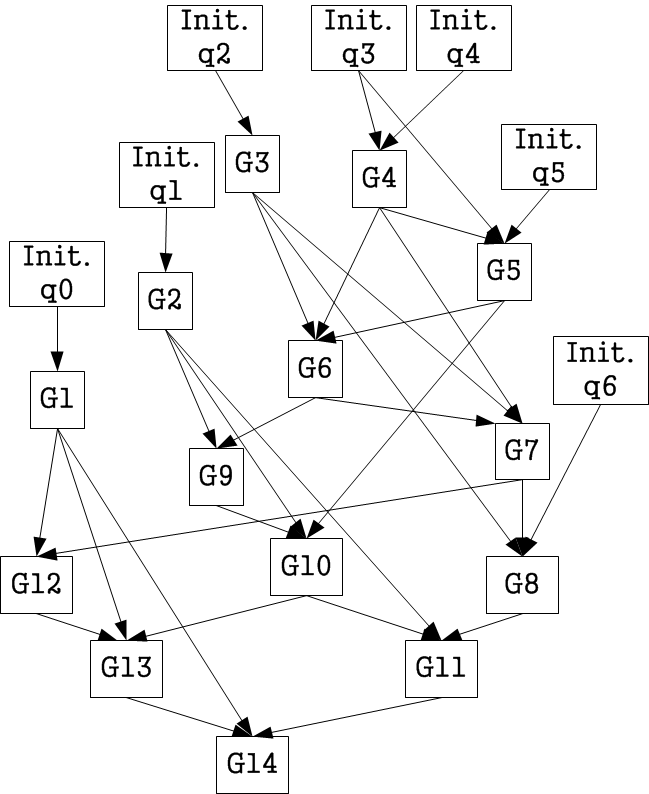
We convert a QASM-described quantum circuit into a data flow-based weighted directed graph, which is called Quantum Operation Dependency Graph (QODG) and shown in Figure 8. In this graph , each operation is denoted using a node , and the data dependency arising from two consecutive operations on a same qubit, e.g., followed by , is represented using a directed edge . and are the node set and edge set of , respectively. We also define and as the collection of edges that exhibits true and name dependency, respectively. represents the starting time of operation and indicates its latency. The scheduling objective is to minimize the total circuit latency (Formula 1) while preserving the data dependency between operations (Formula 2).
| (1) |
subject to
| (2) |
Note that two CNOT gates which share the same control or the same target qubit are commutable, meaning that they can be executed in any order except in parallel. This commutation property has not been considered in previous works (lin2015paqcs, ; metodi2006scheduling, ; whitney2007automated, ; dousti12min, ; yazdani2013quantum, ; bahreini2015minlp, ; balensiefer2005quale, ; dousti2013leqa, ; dousti2014squash, ; ahsan2015architecture, ; heckey2015compiler, ). In this paper, we take commuted CNOT gates into account and replace the optimization condition 2 with conditions 3 and 4:
| (3) |
| (4) |
With respect to different dependencies, the scheduler will exploit parallelism and output the operation sequence with timing information, which is an as-soon-as-possible (ASAP) schedule. An as-late-as-possible (ALAP) schedule can be also easily implemented by scheduling operations in the reverse order (Figure 8).
4.2. Placing and routing qubits
The QAP-model for initial placement of qubits: The goal of qubit placement is to find an optimal initial placement of the qubits that minimizes communication overhead. Similar to the placement approaches in (bahreini2015minlp, ; dousti2014squash, ; shafaei2014qubit, ), the initial placement problem is formulated as a quadratic assignment problem (QAP) with the communication overhead represented using the Manhattan distance:
| (5) |
subject to
| (6) |
| (7) |
| (8) |
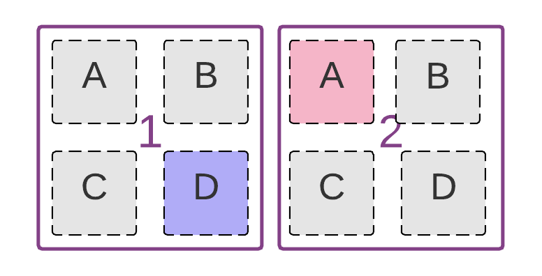
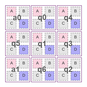
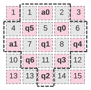
where () is the number of locations(qubits), or indicates whether qubit is assigned to location or not, is the cost of separately assigning qubit and to locations and . is the Manhattan distance between locations and , and is the number of interactions between qubits and in the circuit. Constraints 6 and 7 ensure a one-to-one mapping from qubits to locations. A location is a tile in the tile-based architecture and a data patch in the checkerboard architecture. For instance, the initial placements of the Steane encoding circuit in the tile-based architecture and the checkerboard architecture are shown in Figure 9.
In this paper, the scheduling and QAP models are solved with integer linear programming (ILP). The scheduling uses the linearization method by (richards2002spacecraft, ), and the QAP uses the method proposed by (kaufman1978algorithm, ). ILP can only solve small-scale problems in reasonable time as the ones used in this paper. Even though for near-term implementation in FT quantum computing, these numbers largely suffice. For large-scale circuits, one can either partition a large circuit into several smaller ones or apply heuristic algorithms to efficiently solve these mapping models (metodi2006scheduling, ; whitney2007automated, ; dousti12min, ; bahreini2015minlp, ; balensiefer2005quale, ; dousti2013leqa, ; ahsan2015architecture, ).
The routing algorithm: The introduced two SC qubit architectures require routing of qubits, which involves finding communication paths and inserting the corresponding movement operations, for instance by means of the SWAP operations. An efficient routing should minimize the number of inserted movement operations as well as the increased latency. In this paper, qubits are routed based on a sliding window (buffer) principle as shown in Algorithm . The algorithm will find a path for the first not NN instruction- i.e. CNOT operation in which qubits are not NN- inside the buffer. We adopted the breadth-first search (BFS) algorithm to find all possible shortest paths. Then, in order to select the communication path the algorithm looks back and forward. The look-back finds the maximum interleaving of movement instructions (SWAPs) with previous instructions. The look-ahead will look how the positions of the qubits involved in a certain path is changed and how it affects future two-qubit operations; that is, we want to avoid to move away qubits that are already close to each other and need to interact in the future. Once the path is selected, the instructions inside the buffer will be rescheduled using the ASAP strategy. Then the buffer will output routing instructions and will be fed with new ones. This process repeats until all CNOT gates can be performed in the pre-defined qubit architecture.
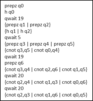
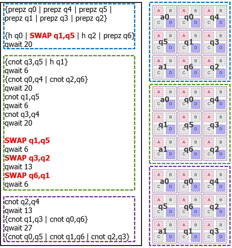
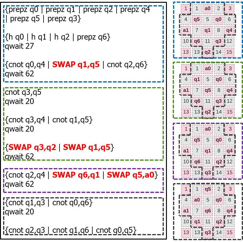
The results of routing the Steane encoding circuit onto the tile-based and checkerboard architectures are shown in Figure 10 and Figure 11, respectively. The inputs of the routing process include 1) the pre-scheduled circuit using an ALAP approach in Figure 8; 2) the initial placement in a pre-defined architecture in Figure 9. The routing process selects the communication path and inserts SWAP operations when two qubits for a coming CNOT gate are not neighbours and then the qubit layout is changed. The final circuits and the intermediate qubit layouts after a full mapping procedure on the tile-based architecture and the checkerboard architecture are shown in Figures 10 and 11 respectively. Note that the operations inside each dashed block will be executed on the qubit layout marked in the same color and the current layout will be transformed into the next one after performing the inserted SWAP operation(s). Note that the final circuits after routing are totally different from the original circuit with an ALAP scheduling. This is because the operations inside each routing buffer has been rescheduled using an ASAP approach.
5. Metrics and benchmarks
In order to evaluate the impact of the mapping passes as well as the proposed qubit plane architectures we define the following metrics:
Qubit efficiency : It is calculated as ; where # AllQubits refers to the total number of logical qubits in a predefined qubit architecture for executing a quantum algorithm, including both logical data qubits and logical ancilla qubits, and # Data is the number of logical data qubits.
Circuit latency: It is the total execution time of a quantum algorithm in SC cycles. Even though reducing the circuit latency may have an overall negligible impact on the exponential performance improvement, it may be important for the algorithms with polynomial speedup. More importantly, shorter latency will also decrease the failure rate of the executed circuit.
Latency overhead: It is the percentage of latency used for moving qubits, and it is calculated as ; where and are the circuit latency with and without considering routing qubits, respectively.
Operation overhead: It is the percentage of inserted movement operations and it is calculated as ; where # Gates is the number of operations of the quantum algorithm which has not been routed (see Table 2) and # SWAPs is the total number of SWAP operations that are inserted for routing qubits. Reducing the number of operations for qubit communication helps to improve the computation fidelity.
Communication overhead: It is expressed in terms of both operation overhead and latency overhead.
The benchmarks used for this mapping evaluation are shown in Table 2 from Qlib (lin2014qlib, ) and RevLib (miller2003transformation, ). These circuits are decomposed into ones which only contain the gates from the fault-tolerantly implementable universal set Pauli, on surface codes. We characterize these benchmarks in terms of percentage of CNOT gates , percentage of edges which have name dependency () in the QODG , and percentage of expensive and gates . The first two benchmarks are encoding circuits of different QEC codes which are used for preparing magic states on SC (fowler2012surface, ). Table 2 also shows the size () of a qubit plane architecture, where and represent the number of data qubits in the axis and axis of the defined qubit plane architecture, respectively.
| Benchmarks | # Qubits | # Gates | #CNOT | Rcg% | Rcd% | Rtsg% | Size |
|---|---|---|---|---|---|---|---|
| 7-enc | 7 | 21 | 12 | 52.38 | 42.55 | 0 | 33 |
| 15-enc | 15 | 53 | 35 | 64.15 | 60.17 | 0 | 44 |
| Adder0-5 | 16 | 306 | 126 | 41.18 | 26.1 | 48.0 | 44 |
| Adder1-8 | 18 | 289 | 129 | 44.64 | 22.38 | 45.3 | 55 |
| Adder1-16 | 34 | 577 | 257 | 44.54 | 22.16 | 44.9 | 66 |
| Multiply4 | 21 | 1655 | 722 | 43.63 | 18.20 | 44.4 | 55 |
| Shor15 | 11 | 4792 | 1788 | 37.31 | 21.03 | 48.4 | 43 |
| sqrt7 | 15 | 7630 | 3089 | 40.48 | 6.41 | 43.72 | 44 |
| sqrt8 | 12 | 3009 | 1314 | 43.67 | 4.63 | 43.50 | 43 |
| ham7 | 7 | 320 | 149 | 35.63 | 5.67 | 41.56 | 33 |
| hwb5 | 5 | 233 | 107 | 45.92 | 5.52 | 42.06 | 32 |
| hwb6 | 6 | 1336 | 598 | 44.76 | 5.26 | 42.96 | 32 |
| hwb7 | 7 | 6723 | 2952 | 61.60 | 4.64 | 43.62 | 33 |
| rd73 | 10 | 230 | 104 | 45.22 | 4.61 | 42.61 | 43 |
| rd84 | 15 | 343 | 154 | 44.90 | 4.63 | 42.86 | 44 |
6. Results
We map the benchmarks shown in Table 2 onto the two introduced qubit architectures using the proposed mapping passes. As shown in Table 1, the execution time of different operations is determined by the code distance which is a tunable parameter of the mapping procedure. In this section, only the mapping results for distance- and distance- planar SC are presented, the results for other distances will be similar.
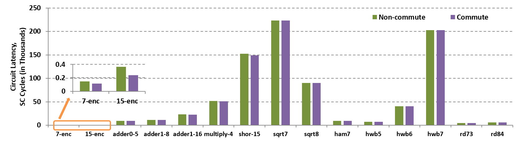
We first analyze the impact of the CNOT commutation property (Section 4.1) on the latency of scheduled quantum circuits. We only show the results for the ALAP scheduling as they are similar to the ASAP scheduling. Figures 12 ( 13) compares the proposed scheduling models for distance (distance ) with and without taking the commutation property into account. For the encoding circuits, the scheduling considering commutation can significantly reduce the circuit latency, () for 7-enc and () for 15-enc, compared to the scheduling without considering commutation. This is because they have a high percentage of commutable CNOT gates () meanwhile the percentage of expensive gates () is much lower (). In contrast, for the other benchmarks the benefit of considering commutation is negligible, up to () for adder0-5.
Furthermore, we perform the full mapping procedure proposed in Section 4, including scheduling, placement and routing, on both the tile-based architecture (t-arch) and the checkerboard architecture (c-arch). The scheduling is implemented by the ALAP approach with considering commutation property. The initial placement is achieved by either the smart approach based on Manhattan distance or the naive method which places qubits in order. Note that the effect of initial placement is not always important (lin2015paqcs, ), depending on the benchmarks (see Appendix D). In this section, the best mapping result of the above two placement approaches for each benchmark is chosen.
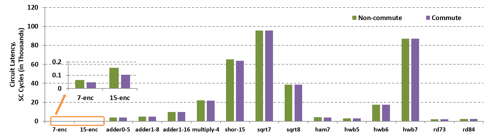
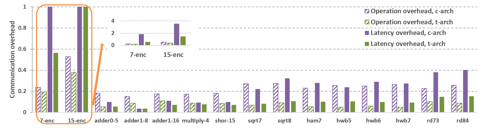
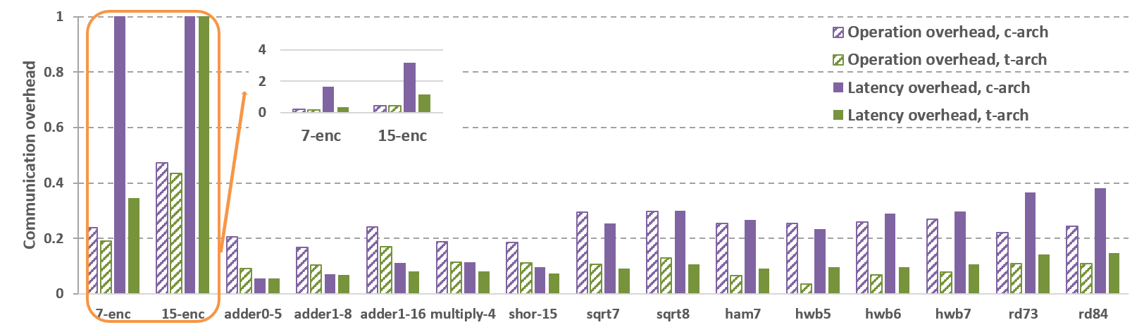
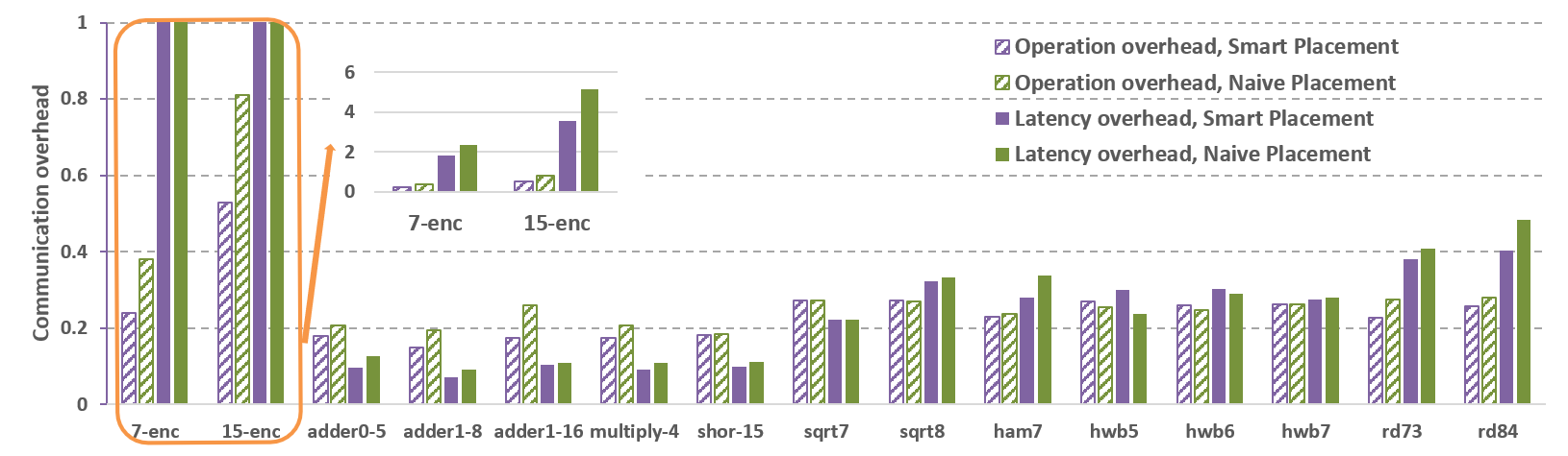
Communication overhead: As mentioned previously, the mapping process results in an increase of the number of quantum operations (operation overhead) as well as in an increase in the circuit latency (latency overhead). We evaluate the communication overhead of mapping quantum circuits on different qubit plane architectures, namely the tile-based architecture (t-arch) and the checkerboard architecture (c-arch). Figure 14 and 15 show the comparison between t-arch and c-arch for distance and surface codes, respectively. The mapping results for both distances are similar and the t-arch achieves less communication overhead because it has a higher number of nearest neighbours.
The operation overhead in the t-arch compared to the c-arch is reduced by (7-enc) up to (hwb5) for and by (15-enc) up to (hwb5) for . The latency overhead when mapping on the t-arch shows a reduction of (adder1-8), (multiply-4) and up to (7-enc) for distance 3. And (adder1-8), (shor-15) and up to (7-enc) for distance 7. Note that this latency reduction is not only due to the less number of movement operations but also due to the use of much faster movements (t-SWAP) although the CNOT gates (t-CNOT) are slightly slower.
Qubit efficiency: As mentioned in Section 3, and of the total number of patches are used for allocating logical data qubits in the tile-based architecture and the checkerboard architecture, respectively. Therefore, the qubit efficiency in the t-arch is and the qubit efficiency in the c-arch is .
Based on the above observations, we can conclude that although the tile-based architecture is less qubit efficient than the checkerboard architecture, it can also substantially reduce the communication overhead in terms of operation overhead (up to ) and latency overhead (up to ). As we mentioned previously, decreasing the communication overhead helps to improve the computation fidelity. Therefore, one may have to compromise between qubit efficiency and communication overhead for the realization of quantum algorithms.
7. Conclusion
We have proposed two SC qubit plane architectures to efficiently support the execution of lattice surgery-based quantum circuits. We developed a full procedure for mapping small-scale quantum algorithms onto these two SC architectures. The experimental results show the following observations. First, the proposed scheduling considering the commutation property provides faster circuit execution than the scheduling without considering commutation. Secondly, the mapping procedure causes communication overhead in terms of both operation overhead and latency overhead. Moreover, the communication overhead highly depends on how qubits are organized and moved, that is, the qubit plane architectures. The tile-based architecture considerably decreases the number of movements and also supports faster execution compared to the checkerboard though it is less qubit-efficient.
As future work, we will focus on heuristic scheduling and placement algorithms as well as different routing techniques for large-scale quantum benchmarks. Furthermore, we will consider the dynamics of quantum computation such as magic state distillation for or gates and qubit routing for performing ‘neighbouring’ CNOT gates. Then we will investigate their implications on quantum circuit mapping. In addition, we will investigate different qubit architectures, for instance, an architecture with specialized communication channels for moving qubits and pre-defined regions for preparing magic states.
References
- (1) P. W. Shor, “Algorithms for quantum computation: Discrete logarithms and factoring,” in SFCS, 1994.
- (2) R. Barends et al., “Superconducting quantum circuits at the surface code threshold for fault tolerance,” Nature, vol. 508, no. 7497, pp. 500–503, 2014.
- (3) R. Versluis et al., “Scalable quantum circuit and control for a superconducting surface code,” arXiv:1612.08208, 2016.
- (4) C. D. Hill et al., “A surface code quantum computer in silicon,” Science advances, vol. 1, no. 9, p. e1500707, 2015.
- (5) R. Li et al., “A crossbar network for silicon quantum dot qubits,” arXiv:1711.03807, 2017.
- (6) IBM, “Quantum experience.”
- (7) S. Boixo et al., “Characterizing quantum supremacy in near-term devices,” arXiv:1608.00263, 2016.
- (8) E. A. Sete et al., “A functional architecture for scalable quantum computing,” in ICRC, pp. 1–6, IEEE, 2016.
- (9) L. S. Bishop et al., “Quantum volume,” tech. rep., 2017.
- (10) N. M. Linke et al., “Experimental comparison of two quantum computing architectures,” Proceedings of the National Academy of Sciences, p. 201618020, 2017.
- (11) T. S. Metodi et al., “Scheduling physical operations in a quantum information processor,” in SPIE, 2006.
- (12) M. Whitney et al., “Automated generation of layout and control for quantum circuits,” in CF, 2007.
- (13) M. J. Dousti and M. Pedram, “Minimizing the latency of quantum circuits during mapping to the ion-trap circuit fabric,” in DATE, 2012.
- (14) M. Yazdani et al., “A quantum physical design flow using ilp and graph drawing,” Quantum information processing, vol. 12, no. 10, pp. 3239–3264, 2013.
- (15) T. Bahreini and N. Mohammadzadeh, “An minlp model for scheduling and placement of quantum circuits with a heuristic solution approach,” JETC, vol. 12, no. 3, p. 29, 2015.
- (16) A. Lye et al., “Determining the minimal number of swap gates for multi-dimensional nearest neighbor quantum circuits,” in ASP-DAC, pp. 178–183, IEEE, 2015.
- (17) R. Wille et al., “Look-ahead schemes for nearest neighbor optimization of 1d and 2d quantum circuits,” in ASP-DAC, pp. 292–297, IEEE, 2016.
- (18) A. Farghadan and N. Mohammadzadeh, “Quantum circuit physical design flow for 2d nearest-neighbor architectures,” International Journal of Circuit Theory and Applications, vol. 45, no. 7, pp. 989–1000, 2017.
- (19) IBM, “Qiskit, quantum information software kit.”
- (20) A. Zulehner et al., “An efficient methodology for mapping quantum circuits to the ibm qx architectures,” arXiv:1712.04722, 2017.
- (21) M. Siraichi et al., “Qubit allocation,” in ACM-CGO, pp. 1–12, 2018.
- (22) D. Venturelli, M. Do, E. Rieffel, and J. Frank, “Compiling quantum circuits to realistic hardware architectures using temporal planners,” Quantum Science and Technology, vol. 3, no. 2, p. 025004, 2018.
- (23) D. Ristè et al., “Detecting bit-flip errors in a logical qubit using stabilizer measurements,” Nature communications, vol. 6, no. 6983, 2015.
- (24) J. Kelly et al., “State preservation by repetitive error detection in a superconducting quantum circuit,” Nature, vol. 519, no. 7541, pp. 66–69, 2015.
- (25) M. A. Nielsen and I. L. Chuang, Quantum computation and quantum information. Cambridge university press, 2010.
- (26) S. Balensiefer et al., “Quale: quantum architecture layout evaluator,” in SPIE, 2005.
- (27) M. J. Dousti and M. Pedram, “Leqa: latency estimation for a quantum algorithm mapped to a quantum circuit fabric,” in DAC, 2013.
- (28) M. J. Dousti et al., “Squash: a scalable quantum mapper considering ancilla sharing,” in GLSVLSI, 2014.
- (29) M. Ahsan, Architecture Framework for Trapped-Ion Quantum Computer based on Performance Simulation Tool. PhD thesis, Duke University, 2015.
- (30) J. Heckey et al., “Compiler management of communication and parallelism for quantum computation,” in ASPLOS, 2015.
- (31) C.-C. Lin et al., “Paqcs: Physical design-aware fault-tolerant quantum circuit synthesis,” IEEE Transactions on VLSI Systems, vol. 23, no. 7, pp. 1221–1234, 2015.
- (32) S. B. Bravyi and A. Y. Kitaev, “Quantum codes on a lattice with boundary,” arXiv:9811052, 1998.
- (33) A. Paler et al., “Synthesis of arbitrary quantum circuits to topological assembly,” Scientific reports, vol. 6, p. 30600, 2016.
- (34) A. Paler et al., “Fault-tolerant, high-level quantum circuits: form, compilation and description,” Quantum Science and Technology, vol. 2, no. 2, p. 025003, 2017.
- (35) A. Paler et al., “Online scheduled execution of quantum circuits protected by surface codes,” arXiv:1711.01385, 2017.
- (36) Javadi-Abhari et al., “Optimized surface code communication in superconducting quantum computers,” in MICRO, pp. 692–705, ACM, 2017.
- (37) C. Horsman et al., “Surface code quantum computing by lattice surgery,” New Journal of Physics, vol. 14, no. 12, p. 123011, 2012.
- (38) A. J. Landahl and C. Ryan-Anderson, “Quantum computing by color-code lattice surgery,” arXiv preprint arXiv:1407.5103, 2014.
- (39) D. Herr et al., “Optimization of lattice surgery is np-hard,” npj Quantum Information, vol. 3, no. 1, p. 35, 2017.
- (40) E. Dennis et al., “Topological quantum memory,” Journal of Mathematical Physics, vol. 43, no. 9, pp. 4452–4505, 2002.
- (41) R. Raussendorf et al., “A fault-tolerant one-way quantum computer,” Annals of physics, vol. 321, no. 9, pp. 2242–2270, 2006.
- (42) A. G. Fowler et al., “Surface codes: Towards practical large-scale quantum computation,” Physical Review A, vol. 86, no. 3, p. 032324, 2012.
- (43) R. Raussendorf and J. Harrington, “Fault-tolerant quantum computation with high threshold in two dimensions,” Physical review letters, vol. 98, no. 19, p. 190504, 2007.
- (44) R. Raussendorf, J. Harrington, and K. Goyal, “Topological fault-tolerance in cluster state quantum computation,” New Journal of Physics, vol. 9, no. 6, p. 199, 2007.
- (45) S. Bravyi and A. Kitaev, “Universal quantum computation with ideal clifford gates and noisy ancillas,” Physical Review A, vol. 71, no. 2, p. 022316, 2005.
- (46) S. Bravyi and J. Haah, “Magic-state distillation with low overhead,” Physical Review A, vol. 86, no. 5, p. 052329, 2012.
- (47) A. M. Meier, B. Eastin, and E. Knill, “Magic-state distillation with the four-qubit code,” arXiv:1204.4221, 2012.
- (48) C. Jones, “Multilevel distillation of magic states for quantum computing,” Physical Review A, vol. 87, no. 4, p. 042305, 2013.
- (49) E. T. Campbell and M. Howard, “Unifying gate synthesis and magic state distillation,” Physical Review L, vol. 118, no. 6, p. 060501, 2017.
- (50) D. Gottesman, “Fault-tolerant quantum computation with higher-dimensional systems,” arXiv:9802007, 1998.
- (51) X. Fu et al., “A heterogeneous quantum computer architecture,” in CF, 2016.
- (52) J. L. Hennessy and D. A. Patterson, Computer architecture: a quantitative approach. Elsevier, 2011.
- (53) A. Shafaei et al., “Qubit placement to minimize communication overhead in 2d quantum architectures,” in ASP-DAC, 2014.
- (54) A. Richards et al., “Spacecraft trajectory planning with avoidance constraints using mixed-integer linear programming,” JGCD, vol. 25, no. 4, pp. 755–764, 2002.
- (55) L. Kaufman and F. Broeckx, “An algorithm for the quadratic assignment problem using bender’s decomposition,” EJOR, vol. 2, no. 3, pp. 207–211, 1978.
- (56) C.-C. Lin et al., “Qlib: Quantum module library,” ACM-JETC, vol. 11, no. 1, p. 7, 2014.
- (57) D. M. Miller et al., “A transformation based algorithm for reversible logic synthesis,” in DAC, pp. 318–323, IEEE, 2003.
- (58) D. Gottesman, “The heisenberg representation of quantum computers,” arXiv:9807006, 1998.
Appendix A Lattice surgery-based CNOT
A CNOT is a gate applying on two qubits, the target qubit undergoes an gate only if the control qubit is in . One way to validate a CNOT implementation is to check the transformation of logical and operators using the Heisenberg representation (gottesman1998heisenberg, ) as follows:
| (9) |
| (10) |
| (11) |
| (12) |
For instance, the CNOT gate transforms an in the control qubit into the target qubit in Equation (9). We can verify the measurement-based procedure (gottesman1998fault, ), which is described by the circuits in Figure 3 and 3, by examining these transformations ((9)-(12)) as shown in Equations (13) and (14) respectively. These equations illustrate how different measurements transform stabilizers and logical operators. ‘C’, ‘T’, and ‘A’ represent the control, target, and ancillary qubit, respectively. ‘S’ and ‘L’ represent the stabilizers and logical operators, respectively. For example, after performing measurements in (13), the stabilizer is transformed into and the logical operator is transformed into . Equations (13) and (14) show that the measurement-based procedure does satisfy the transform relations in Equations (9)-(12) and it is thus equivalent to a CNOT.
| (13) |
|
| (14) |
|
The joint measurement () is realized by merge and split operations using lattice surgery (horsman2012surface, ; landahl2014quantum, ). The basic operations of lattice surgery are to stop measuring some existing stabilizers and start to measure some new stabilizers. For example, the merge operation for on the qubits ‘A’ and ‘C’ in Figure 2 is performed by ceasing to measure and , starting to measure , and , that is, performing rounds of ESM on the merged lattice in Figure 2. This means the two lattices ‘’ and ‘’ are integrated into one single lattice. Similarly, the split operation is implemented by ceasing to measure , and , starting to measure stabilizer and , that is, performing rounds of ESM individually on each lattice ‘’ and ‘’ in Figure 2. The splitting procedure divides the merged lattice back into two lattices. Afterwards, one needs to read out the outcome of each joint measurement for further logical Pauli corrections. The measurement result of is interpreted into () if the number of ‘’ syndromes from the new stabilizers and during the merge is even (odd).
Appendix B Lattice surgery-based movement
The lattice surgery-based joint measurements can be used to ‘move’ logical qubits to other locations. As mentioned previously, the adjacent boundaries should be in both - or -type when performing such a joint measurement. Assuming that the qubit patches in the same row (column) of the tile-based architecture in Figure 5 have (-)type adjacent boundaries, we introduce two basic movements: horizontal movement (Figure 16) and vertical movement (Figure 17). A logical state in can be moved to its horizontally (vertically) adjacent position () by first performing a joint measurement () between and () followed by a () measurement on . This horizontal (vertical) movements mimics the procedure in Equation (15) (Equation (16)), that is, the logical operators in patch are transformed into patch (). It means that the logical state in is moved to patch (). One can progressively move one logical state from one patch to the other by applying these horizontal movements and vertical movements as shown in Figure 18.
| (15) |
| (16) |
Appendix C FT library
After the logical-level mapping, the physical-level mapping becomes trivial for several reasons. First, there is no need to place and route physical qubits since surface codes intrinsically satisfy the 2D NN constraint. Secondly, as discussed in Section 2, each of the universal set of logical operations (preparation, measurement, Pauli, H, CNOT, S and T gates) on planar SC is implemented by a certain series of SC cycles.
As shown in Figure 19, each cycle is composed of two time slots, one purple slot for performing physical single-qubit gates and one gray slot for performing one round of ESM. Depending on the logical operation, a single-qubit gate such as Identity, Pauli gates or H gate needs to be performed during each purple slot. For instance, a logical X gate on the distance- planar surface code (Figure 20) can be realized by one SC cycle, that is, first performing bit-wise physical X gates on qubits (purple slot) and then performing round of ESM (gray slot). Therefore, a library can be built to translate each logical operation into pre-scheduled physical quantum operations. Since the operations in a purple slot are bit-wise and performed in parallel, one only need to pre-schedule the operations of error syndrome measurement.
The ESM circuits for and stabilizers are shown in Figure 1.
One full round of ESM on the distance- planar surface code (Figure 20) is scheduled and performed as follows (in QASM):
{ prepz A2 — prepz A7 — prepz A5}
{ h A2 — h A7 — h A5 — prepz A1 — prepz A3 — prepz A6}
{ cnot A2, D5 — cnot A7, D9 — cnot A5, D7 — cnot D2, A1 — cnot D6, A3 — cnot D8, A6 — prepz A8 — prepz A4}
{ cnot A2, D2 — cnot A7, D6 — cnot A5, D4 — cnot D9, A8 — cnot D3, A3 — cnot D5, A6 — h A4}
{ cnot A2, D4 — cnot A7, D8 — cnot A4, D6 — cnot D1, A1 — cnot D5, A3 — cnot D7, A6 — h A5}
{ cnot A2, D1 — cnot A7, D5 — cnot A4, D3 — cnot D8, A8 — cnot D2, A3 — cnot D4, A6 — measure A1 — measure A5}
{ h A2 — h A4 — h A7 — measure A3 — measure A6 — measure A8}
{ measure A2 — measure A4 — measure A7}
However, a more realistic scheduling needs to consider the underlying hardware constraints such as the allowed primitive operations, their execution time, frequency multiplexing, etc. A scalable scheme for executing the ESM of surface code on superconducting qubits with NN coupling can be found in (versluis2016scalable, ).
Appendix D Initial placements
In this section, we examine how initial placement affects the mapping results.
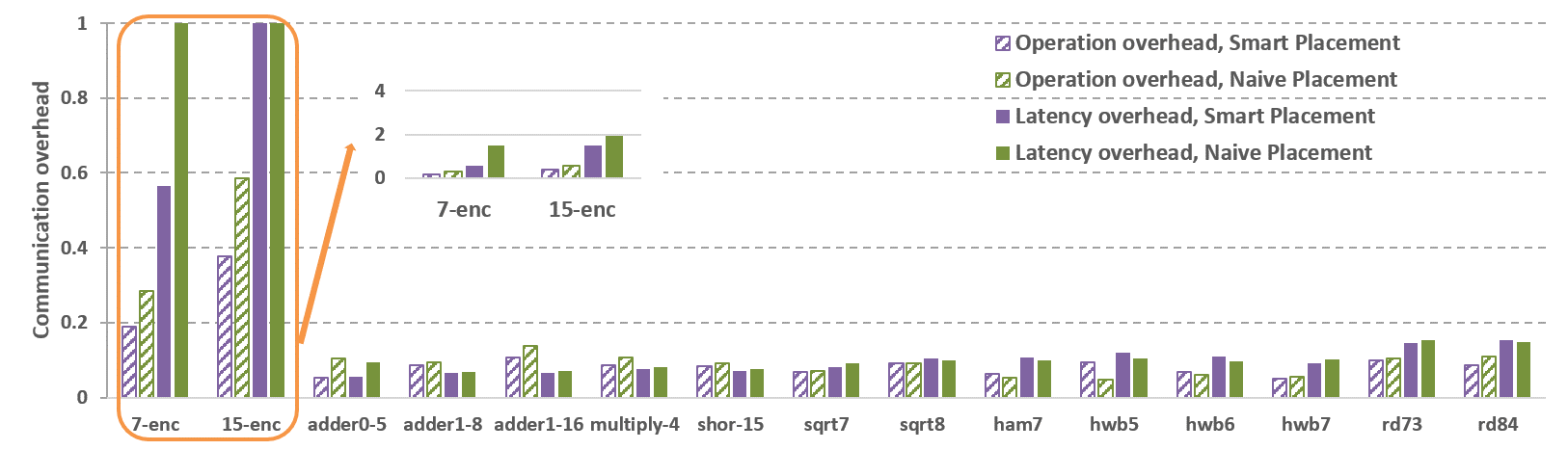
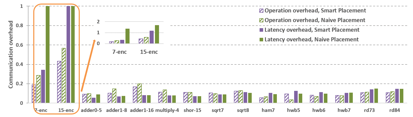
Figures 21 and 22 show the comparison of the proposed smart placement based on Manhattan distance with a naive placement which locates qubits in order, where logical qubits are encoded by the distance- surface code. For some benchmarks, the use of the smart initial placement effectively decreases the operation overhead on both the c-arch and the t-arch, from up to (rd84, adder0-5, multiply-4, rd73, adder1-8, adder1-16, 15-enc) and from up to (adder1-8, hwb7, shor-15, multiply-4, rd84, adder1-16, 7-enc, 15-enc), respectively. Furthermore, the smart placement approach reduces the latency overhead of the c-arch and t-arch by to (rd73, shor-15, rd84, multiply-4, ham7, adder1-8, 7-enc, adder0-5, 15-enc) and by to (shor-15, adder1-16, hwb7, sqrt7, 15-enc, adder0-5, 7-enc), respectively. However, for other benchmarks, the smart placements provide marginal reductions or even increases in communication overhead on both qubit architectures. This is because the position of the qubits will change after each SWAP operation, and the possible benefit of the smart initial placement will progressively disappear as the circuit execution advances.
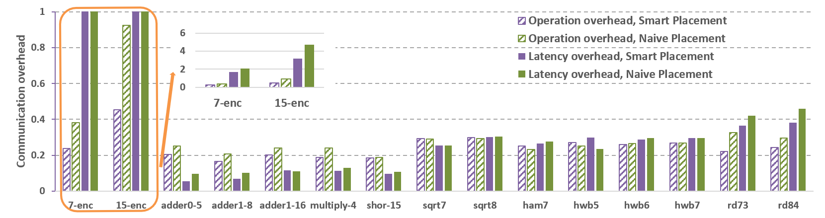
Figures 23 and 24 show similar results for distance- surface code. For some benchmarks, the use of smart initial placements can effectively decrease the communication overhead compared to naive placements. The smart initial placement decreases the operation overhead on the c-arch and the t-arch, from up to (adder1-16, rd84, adder0-5, adder1-8, 7-enc, 15-enc) and from up to (adder0-5, rd84, ham7, adder1-16, multiply-4, 15-enc, adder1-8, 7-enc), respectively. Moreover, the smart placement approach reduces the latency overhead of the c-arch and t-arch by to (shor-15, multiply-4, rd73, rd84, 7-enc, adder1-8, 15-enc, adder0-5) and by to (rd73, adder1-8, 15-enc, adder0-5, 7-enc), respectively. However, for other benchmarks, the benefits from smart initial placements disappear on both qubit architectures.