Experimental observation of bound states of 2D Dirac electrons on the surface of topological insulator Bi2Se3
Abstract
Topologically protected surface states of three-dimensional topological insulators provide a model framework for studying massless Dirac electrons in two dimensions. Usually a step on the surface of a topological insulator is treated as a scatterer for the Dirac electrons, and the study of its effect is focused on the interference of the incident and scattered electrons. Then a major role plays the warping of the Dirac cone far from the Dirac point. Here we experimentally demonstrate the existence of another significant effect near the Dirac point brought about by the presence of steps. Namely the band bending in the vicinity of steps leads to formation of 1D bound states in the corresponding potential wells. We report the observation of bound states in such potential wells in our scanning tunneling microscopy and spectroscopy investigation of the surface of the topological insulator Bi2Se3. Numerical simulations support our conclusion and provide a recipe for their identification.
Recently, a number of solid state systems have been used as model systems for investigating exotic particle physics for quantum field theory and high-energy physics. Of great interest in this respect are Dirac materials Wehling2014 . Their electronic excitations obey the Dirac equation, in place of the Schroedinger one. This opens up a possibility to study quasi-relativistic physics in a convenient tunable solid-state setting. In particular, graphene and, more recently, topological insulators provide a model framework for studying massless Dirac electrons in two dimensions.
Three-dimensional topological insulators are characterized by the presence of gapless surface states on the background of an insulating bulk review . The existence of these states is governed by the nontrivial value of the topological invariant. In the prototypical topological insulator Bi2Se3 Zhang2009 the topologically protected surface states form a cone in -space. The apex of the cone (the Dirac point) is located at the -point of the surface Brillouin zone, its energy being within the bulk band gap. In the vicinity of the Dirac point the Bi2Se3 surface states can be described by a model Dirac Hamiltonian Zhang2009 . Here is the Pauli matrices vector, is the wave vector, eVnm defines the Fermi velocity.
Massless Dirac electrons possess a number of peculiar properties. For instance, they can travel without reflection through a potential step (Klein tunneling Klein1929 ; Katsnelson2006 ). It is generally accepted that due to the Klein tunneling the confinement of massless fermions by means of purely electrostatic potential is not possible. It is true in a one-dimensional (1D) case, however for a 2D Dirac system with a 1D potential, states localized in one direction (perpendicular to the potential well or barrier) exist Pereira2006 ; Tudorovskiy2007 . The issue of Dirac electrons confinement continues to attract considerable attention from theorists Yampolskii2008 ; Yokoyama2010 ; Seshadri2014 ; Hartmann2017 . Experiments in this area have been mostly concentrated on graphene: from Klein tunneling Young2009 to lithographically defined quantum dots Ponomarenko2008 and chemically synthesized flakes Subramaniam2012 . More recently, quasi-bound states were observed by means of scanning tunneling microscopy in electrostatically defined quantum dots Gutierrez2016 ; Lee2016 . Current distribution in one-dimensional graphene edge channels was investigated in transport measurements Allen2016 .
Topologically nontrivial systems offers an extensive playground for studying exotic quasiparticle physics. A prime example of the reach variety of physical properties in these systems are sister compounds Bi2Se3 and Bi2Te3, both topological insulators. The Dirac cone warping and the Dirac point position in the bulk valence band in the latter substance cause a dramatic difference in the behavior of the topologically protected surface states. As shown by tight binding calculations Kobayashi , edge states could form on the surface steps of Bi2Te3, whereas no such states are expected on Bi2Se3. These calculations do not, however, take into account the 1D potential wells for the Dirac electrons that arise on the surface of the topological insulator Bi2Se3 as band bending occurs near surface steps Fedotov2017 .
Steps on the surface of topological insulators are interesting objects of experimental Alpichshev ; Interf1 ; Interf2 ; Dmitriev ; Fedotov2017 ; Seo2010 ; Bauer2016 as well as theoretical Yokoyama2010 ; Seshadri2014 ; Kobayashi ; Xu2018 ; Moon ; Narayan2014 ; Alos2013 ; Wang2010 ; Biswas2011 ; Liu2012 ; Zheng2012 ; An2012 investigation. Edge states were found on steps in crystalline topological insulators crystalTI and Weyl semimetals Weyl1 ; Weyl2 ; Weyl3 . Topological insulators of higher order revealing hinge states are also at the forefront of topological insulator research HighTI .
Most STS studies of surface steps in bismuth chalcogenide systems focus on the surface states scattering and interference patterns Interf1 ; Interf2 . Alpichshev et al. Alpichshev observed an accumulation of LDOS near a step on the surface of topological insulator Bi2Te3 by means of STS. This accumulation was ultimately attributed to a contribution from the states on the side surface of the step AlpichshevDiss .
Formation of waveguide states on the side surface of a step in Bi2Se3 was discussed theoretically in Moon using an optical analogy on the basis of the lower Fermi velocity of the topologically protected surface states on the side surface obtained in DFT calculations.
Other theoretical approaches include treating the step as a -function potential barrier Biswas2011 ; Liu2012 ; Zheng2012 ; An2012 ; Xu2018 . A barrier potential at the step results in bound states formation, but branches of point in the opposite direction compared to the states in a potential well discussed here. Papers Biswas2011 ; Liu2012 ; Zheng2012 ; An2012 focus on the scattering of the surface states rather than the formation of bound states.
Here we report direct observation of bound states in potential wells formed in the vicinity of steps on the surface of the topological insulator Bi2Se3. We employ scanning tunneling microscopy and spectroscopy (STM/STS) to image the spatial distribution of LDOS and numerical modeling to support our findings.
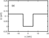
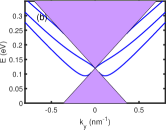
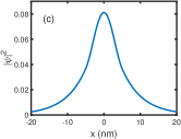
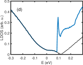
Let us briefly remind the specifics of bound states formation in a massless Dirac system using an exactly solvable model of a rectangular potential well. Following Pereira2006 ; Tudorovskiy2007 , we are considering a system with a Hamiltonian
| (1) |
where is a 1D rectangular potential well running along the axis (Fig. 1(a))
Since is invariant under translations along the axis, is a good quantum number. Inside the well the wave function is a combination of and outside the well . For and we have and correspondingly. The continuity condition for the wave function at leads to an equation for of the states localized in the direction in the quantum well
| (2) |
For each value of equation (2) has solutions , that give us branches of the bound 1D states in the potential well. Corresponding energy dispersions are given by .
The dispersions of three lowest branches of these states calculated using Eq. (2) for eV, nm are shown in Fig. 1(b). The shaded area represents the continuum of the 2D states forming the Dirac cone. Attached to it are the branches of the bound 1D states. The lowest branch has a minimum, that gives rise to a pronounced peak in the density of states. The second branch is attached to the Dirac point. For a square potential such a branch exists independently of the potential strength, for a sufficiently weak potential it is the lowest branch. This may be also the case for other potential shapes as is claimed in Xu2018 .
The calculated local density of states (LDOS) in the center of the potential well is shown in Fig. 1(d) (solid line). It deviates considerably from the V-shape of the unperturbed LDOS. The minimum flattens out and a maximum appears. The contribution of delocalized states to the LDOS is shown in Fig. 1(d) by a dashed line. We see that the sharp feature is due to the local density of the bound states. The probability density of a bound state from the lowest branch is shown in Fig. 1(c).
Thus, the signatures of the bound states in the LDOS are disappearance and flattening of the sharp V-shaped minimum, representing the Dirac cone apex, and formation of a single or multiple peaks or step-like features (see also Yampolskii2008 ). STM can be used to search for such features in the tunneling spectra. 1D potential wells similar to the one discussed above arise due to the band bending in the vicinity of extended surface defects of a topological insulator, e. g. Bi2Se3. Below we report our observations of bound states in such potential wells Fedotov2017 .
For the experimental search for the bound states we performed spatially resolved scanning tunneling microscopy and spectroscopy measurements on the surface of Bi2Se3 samples cleaved in situ. All the measurements were done at liquid helium temperature in the UHV conditions (typical base vacuum Torr). Pt-Rh tips were used, their quality was checked on Au foil. If needed, we performed a tip recovery procedure which included briefly dipping the tip into the Au foil followed by the tip control procedure. The curves of the tunneling junction (tunneling spectra) were obtained by numerically differentiating measured curves. To account for the band bending and extract information about the local potential we use the normalization method described in Ref. Fedotov2017 . The local potential is obtained as the overall shift of the normalized curve.
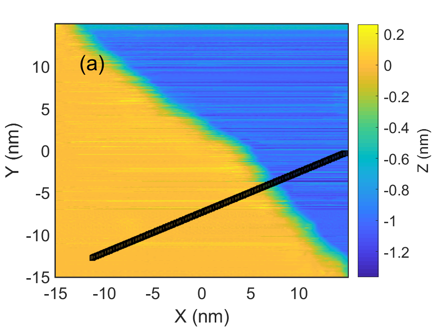
Bi2Se3 is a layered compound that consists of quintuple layers (QL) Se-Bi-Se-Bi-Se bound one with another by van der Waals interaction. When Bi2Se3 is cleaved, high steps ( nm) are formed if one or more quintuple layers are torn. An STM image of such a step is shown in Fig. 3(a). The step height nm corresponds to 1 QL. In the vicinity of these steps on Bi2Se3 surface on a nm scale a meV shift of the chemical potential occurs Dmitriev ; Fedotov2017 , thus forming a potential well for the Dirac electrons.
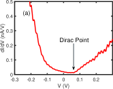
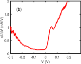
A typical differential tunneling conductance () curve taken far from any defects is presented in Fig. 2(a). As the Dirac point of the Bi2Se3 surface states lies within its bulk band gap, it corresponds to the V-shaped minimum of the curve (shown with an arrow). A differential tunneling conductance curve taken on a step is shown in Fig. 2(b). Apart from an overall shift in voltage, corresponding to the local potential, it shows significant change in shape in comparison with the spectrum away from defects (Fig. 2(a)). Specifically, the V-shaped minimum corresponding to the Dirac point flattens out and a sharp rise with a maximum appears at the side of the flattened region of the curve. From the comparison with the model predictions it is evident, that these changes of LDOS are in agreement with the expected effect of a potential well. In particular the sharp feature corresponds to bound states formation.
A spatially resolved STS map taken along a line (black squares in Fig. 3(a)) across the step in Fig. 3(a) is shown in Fig. 3(b). Approximate positions of the Dirac point and bulk band edges (depicted by white dashed lines in Fig. 3(b)) are determined as in Ref. Fedotov2017 . A 0.15 V deep and nm wide potential well forms due to the band bending in the vicinity of the step (which is located at nm). A horizontal feature of the normalized appears in the potential well region at eV. This feature in the STS map corresponds to a maximum of the differential tunneling conductance, such as the one in Fig. 2(b). This maximum is a feature of the LDOS of the sample and not of the tip as it is absent on both sides of the step. Moreover, it does not correspond to a dangling-bond state or a state of an atom adsorbed on the step edge because such states do not spread over distances of nm. We observe this behavior in different points along a step and in multiple samples. For instance, Figs. 2 and 3 were obtained on different samples. We argue that this horizontal feature is evidence of formation of bound states in a system of massless 2D electrons, namely the topologically protected surface states of a topological insulator.
To justify our interpretation we compare the experimental spatially resolved STS data in the potential well near the surface step in Fig. 3 with the spatial distributions of numerically calculated local density of states of 2D massless Dirac electrons in a one-dimensional potential of the same shape. We perform our calculations based on the model Dirac Hamiltonian Eq (1). The potential is assumed to be constant along the axis in our approximation, so that the wave function and the 2D Dirac equation is reduced to a 1D equation for each value of . We numerically solve the corresponding equation by a symmetric finite difference method with periodical boundary conditions. Grid discretizations of such equations produce spurious solutions, a problem known as fermion doubling. One of the ways to avoid the fermion doubling is to add a Wilson mass term doubling . This is the method we use in this work.
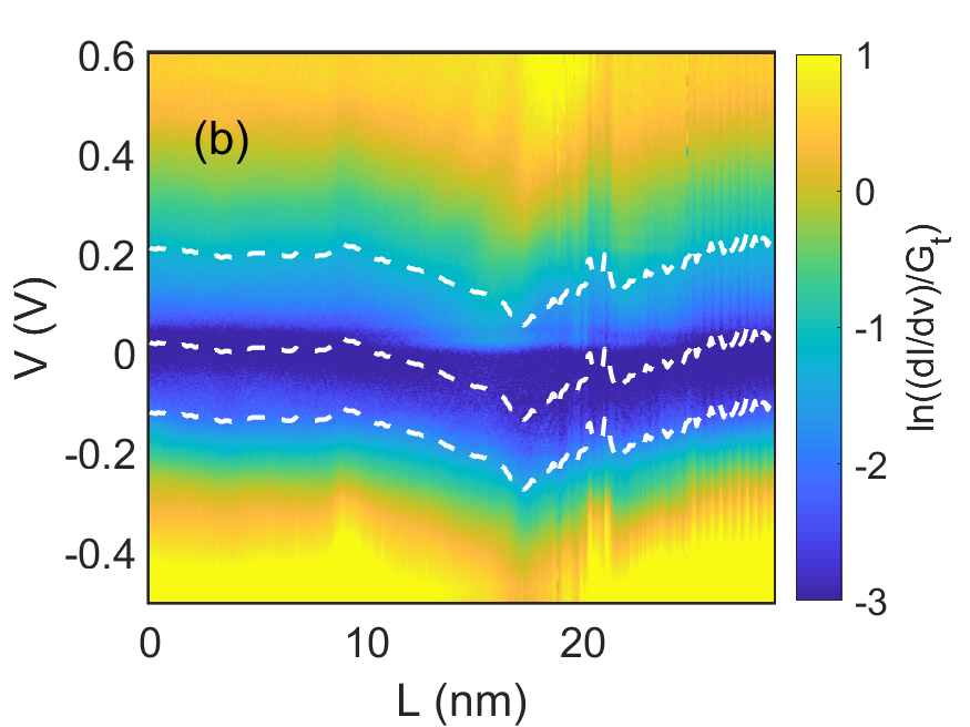
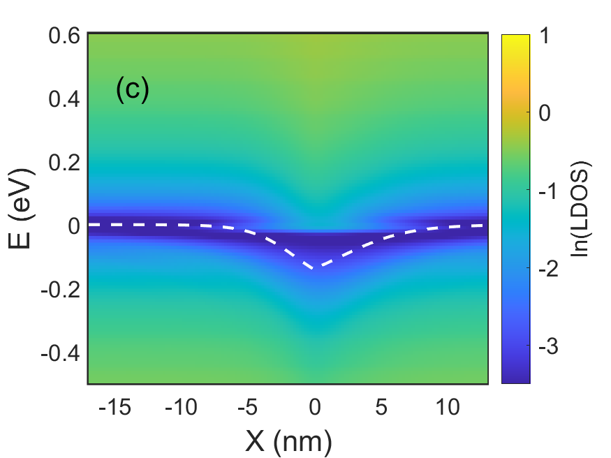
The numerically calculated spatial distribution of the local density of states in the quantum well, corresponding to the potential near the step in Fig. 3(a), is shown in Fig. 3(c). The white dashed line depicts the potential profile used for the calculations. The results are in reasonable qualitative as well as quantitative agreement with the experimental distribution both in energy and in space despite the absence of any fitting parameters. Namely, a sharp feature appears in the potential well region in the calculations as well as in the experimental results. The energy dispersion resulting from the numerical simulation exhibits similar features as the one in Fig. 1(b). Namely, branches of bound states arise, attached to the Dirac cone of the 2D delocalized states. The local density of these states produces the horizontal feature in the spatial distribution of LDOS. Similar features can be observed in the potential wells near other types of extended defects.
Formation of such bound states (or waveguide states) was discussed theoretically in Yokoyama2010 ; Seshadri2014 in the case of topological insulators. These two papers focus on the branches of the bound states that connect to the Dirac point. We find however that for the typical parameters of the potential wells in our case (100 mV, 10 nm) lower lying branches exist, that provide a larger peak-like contribution to the LDOS. Note that energy dispersion and properties of such states depend on the parameters of the potential and may vary e. g. with step height or defect type.
The increase of LDOS near a step on the surface of topological insulator Bi2Te3 observed by Alpichshev et al. Alpichshev is due to a purely geometrical effect associated with the presence of an edge connecting two surfaces at an angle AlpichshevDiss . Such an effect is also reproduced by numerical simulation FedotovZZ2018 . Thus, this increase of LDOS does not correspond to a bound state. In our case the bound state forms in a potential well on the surface of Bi2Se3 and is not intrinsically linked to the presence of the step.
The comparatively large localization length of the states we observe on the upper surface of the step implies that they are not a manifestation of the states forming on the side surface of a step discussed in Moon .
In other papers Biswas2011 ; An2012 the surface step is modeled as a scattering -function barrier. We are considering only the experimentally observed potential wells formed on both sides of the step. The rationale behind this approach is that the topologically protected surface states flow around the step. To take the effect of the step into account more accurately one needs to consider a three-dimensional model. Note that a barrier potential at the step also results in bound states formation, but branches of point in the opposite direction. Correspondingly the energy distribution of LDOS is reversed.
The fact that steps are always present at the surface of a topological insulator inevitably leads to the presence of the bound states. The role of such states is especially important when the Fermi levels is near the Dirac point where the density of states is low. In particular, they may be involved in scattering of surface electrons, which is associated with a change in the spin direction. So the spin texture associated with such defects is an interesting question. Thus the formation of bound states at the extended defects of the surface (especially surface steps) of topological insulators may result in additional conductivity and scattering channels and has to be taken into account when considering prospects of topological insulator based quantum devices.
In conclusion, we experimentally observe formation of one-dimensional bound states of two-dimensional massless Dirac electrons in potential wells in the vicinity of surface steps on the Bi2Se3 topological insulator. Numerical simulations support this conclusion and provide a recipe for their identification. The states form branches attached to the Dirac cone and can be identified on spatially resolved STS maps as sharp horizontal features with characteristic length nm.
Acknowledgments We are grateful to V.A. Sablikov for valuable discussion. The work was carried out with financial support of RSF (grant 16-12-10335).
References
- (1) T.O. Wehling, A.M. Black-Schaffer, and A.V. Balatsky Advances in Physics 63, 1-76 (2014).
- (2) As a review see: Topological Insulators: Fundamentals and Perspectives, Eds.: Frank Ortmann, Stephan Roche, Sergio O. Valenzuela, Laurens W. Molenkamp, Wiley (2015); Contemporary Concepts of Condensed Matter Science, Eds.: E.Burstein, A.H. Macdonald and P. J. Stiles, Vol. 6, Topological Insulators, Eds.: M. Franz, L. Molenkamp, Elsevier, Oxford, 2013.
- (3) Haijun Zhang, Chao-Xing Liu, Xiao-Liang Qi, Xi Dai, Zhong Fang and Shou-Cheng Zhang, Nat. Phys. 5, 438–442 (2009).
- (4) Klein, O. Z. Phys. 53, 157 (1929).
- (5) M. I. Katsnelson, K. S. Novoselov, and A. K. Geim Nat. Phys. 2, 620–625 (2006).
- (6) J. Milton Pereira, Jr., V. Mlinar, F. M. Peeters, and P. Vasilopoulos Phys. Rev. B 74, 045424 (2006).
- (7) T. Ya. Tudorovskiy, A. V. Chaplik, JETP Lett. 84, 619 (2007).
- (8) Takehito Yokoyama, Alexander V. Balatsky, and Naoto Nagaosa Phys. Rev. Lett. 104, 246806 (2010).
- (9) Ranjani Seshadri and Diptiman Sen Phys. Rev. B 89, 235415 (2014).
- (10) V A Yampol’skii, S Savel’ev and Franco Nori, New J. Phys. 10, 053024 (2008).
- (11) R. R. Hartmann and M. E. Portnoi Scientific Reports 7, 11599 (2017).
- (12) Young, A. F. and Kim, P. Nat. Phys. 5, 222–226 (2009).
- (13) L. A. Ponomarenko, et al. Science 320, 356–358 (2008).
- (14) D. Subramaniam, F. Libisch, Y. Li, C. Pauly, V. Geringer, R. Reiter, T. Mashoff, M. Liebmann, J. Burgdörfer, C. Busse, T. Michely, R. Mazzarello, M. Pratzer, and M. Morgenstern Phys. Rev. Lett. 108, 046801 (2012).
- (15) Christopher Gutiérrez, Lola Brown, Cheol-Joo Kim, Jiwoong Park, and Abhay N. Pasupathy Nat. Phys. 12, 1069 (2016).
- (16) Juwon Lee, Dillon Wong, Jairo Velasco Jr, Joaquin F. Rodriguez-Nieva, Salman Kahn, Hsin-Zon Tsai, Takashi Taniguchi, Kenji Watanabe, Alex Zettl, Feng Wang, Leonid S. Levitov, and Michael F. Crommie Nat. Phys. 12, 1032 (2016).
- (17) M. T. Allen, O. Shtanko, I. C. Fulga, A. R. Akhmerov, K. Watanabe, T. Taniguchi, P. Jarillo-Herrero, L. S. Levitov, and A. Yacoby Nat. Phys. 12, 128 (2016).
- (18) Katsuyoshi Kobayashi Phys. Rev. B 84, 205454 (2011).
- (19) N. I. Fedotov and S. V. Zaitsev-Zotov Phys. Rev. B 95, 155403 (2017).
- (20) A.Yu. Dmitriev, N.I. Fedotov, V.F. Nasretdinova, S.V. Zaitsev-Zotov, Pis’ma Zh. Eksp. Teor. Fiz., 100, 442 (2014); JETP Letters, 100, 398 (2014). DOI: 10.1134/S0021364014180039.
- (21) Zh. Alpichshev, J. G. Analytis, J.-H. Chu, I. R. Fisher, and A. Kapitulnik, Phys. Rev. B 84, 041104(R) (2011).
- (22) Can-Li Song, Lili Wang, Ke He, Shuai-Hua Ji, Xi Chen, Xu-Cun Ma, and Qi-Kun Xue Phys. Rev. Lett. 114, 176602 (2015)
- (23) Tong Zhang, Peng Cheng, Xi Chen, Jin-Feng Jia, Xucun Ma, Ke He, Lili Wang, Haijun Zhang, Xi Dai, Zhong Fang, Xincheng Xie, and Qi-Kun Xue Phys. Rev. Lett. 103, 266803 (2009).
- (24) Jungpil Seo, Pedram Roushan, Haim Beidenkopf, Y. S. Hor, R. J. Cava, and Ali Yazdani1 Nature 466, 343–346 (2010).
- (25) Sebastian Bauer and Christian A. Bobisch Nat. Comms. 7, 11381 (2016).
- (26) Yishuai Xu, Guodong Jiang, Janet Chiu, Lin Miao, Erica Kotta, Yutan Zhang, Rudro R. Biswas, and L. Andrew Wray, New J. Phys. 20 073014 (2018).
- (27) Ch.-Y. Moon, J. Han, H. Lee, and H. J.Choi, Phys.Rev. B 84, 195425 (2011).
- (28) Awadhesh Narayan, Ivan Rungger, Andrea Droghetti, and Stefano Sanvito Phys. Rev. B 90, 205431 (2014).
- (29) M. Alos-Palop, Rakesh P. Tiwari, and M. Blaauboer Phys. Rev. B 87, 035432 (2013).
- (30) Qiang-Hua Wang, Da Wang, and Fu-Chun Zhang Phys. Rev. B 81, 035104 (2010).
- (31) Rudro R. Biswas and Alexander V. Balatsky Phys. Rev. B 83, 075439 (2011).
- (32) Qin Liu, Xiao-Liang Qi, and Shou-Cheng Zhang Phys. Rev. B 85, 125314 (2012).
- (33) Degang Zhang and C. S. Ting Phys. Rev. B 85, 115434 (2012).
- (34) Jin An and C. S. Ting Phys. Rev. B 86, 165313 (2012).
- (35) Sessi P, Di Sante D, Szczerbakow A, Glott F, Wilfert S, Schmidt H, Bathon T, Dziawa P, Greiter M, Neupert T et al. Science 354 1269 (2016).
- (36) X. Li, W. Huang, Y. Lv, K. Zhang, C. Yang, B. Zhang, Y. B. Chen, S. Yao, J. Zhou, M. Lu, L. Sheng et al. Phys. Rev. Lett. 116 176803(2016).
- (37) Z. Fei, T. Palomaki, S. Wu, W. Zhao, X. Cai, B. Sun, P. Nguyen, J. Finney, X. Xu and D. H. Cobden Nature Physics 13 677–682 (2017).
- (38) S. Tang, C. Zhang, D. Wong, Z. Pedramrazi, H. Tsai, C. Jia, B. Moritz, M. Claassen, H. Ryu, S. Kahn et al. Nature Physics 13 683–687 (2017).
- (39) Frank Schindler, Ashley M. Cook, Maia G. Vergniory, Zhijun Wang, Stuart S. P. Parkin, B. Andrei Bernevig, and Titus Neupert Sci. Adv., 4 eaat0346 (2018)
- (40) Zh. Alpichshev (2012) STM and STS studies of electronic states near macroscopic defects in topological insulators (Doctoral dissertation)
- (41) Leonard Susskind Phys. Rev. D 16, 3031 (1977).
- (42) N. I. Fedotov and S. V. Zaitsev-Zotov arXiv:1807.09068.