Search for alternative magnetic tunnel junctions based on all-Heusler stacks
Abstract
By imposing the constraints of structural compatibility, stability and a large tunneling magneto-resistance, we have identified the Fe3Al/BiF3/Fe3Al stack as a possible alternative to the well-established FeCoB/MgO/FeCoB in the search for a novel materials platform for high-performance magnetic tunnel junctions. Various geometries of the Fe3Al/BiF3/Fe3Al structure have been analyzed, demonstrating that a barrier of less than 2 nm yields a tunneling magneto-resistance in excess of 25,000 % at low bias, without the need for the electrodes to be half-metallic. Importantly, the presence of a significant spin gap in Fe3Al for states with symmetry along the stack direction makes the TMR very resilient to high voltages.
pacs:
72.15.-v 85.70.Ay 85.75.DdI Introduction
Spin valves displaying large tunnel magneto-resistance (TMR) have undoubtedly revolutionized the electronics industry and now form the central component of many technologies, the most successful device being the read heads in hard-disk drives TMR300 . Importantly, spin valves are set to become the central component of many devices of the future, such as magnetic random access memories and spin-torque oscillators. The major breakthrough was the fabrication of epitaxial CoFeB/MgO/CoFeB spin valves Yuasa ; Parkin , which exploit coherent electronic tunneling Butler ; Mathon to provide a large TMR even at room temperature. In practical devices the fabrication of CoFeB/MgO/CoFeB spin valves requires the growth of rather complex thin films stacks, including functional layers (e.g. for magnetic pinning) and seed layers necessary for the epitaxial growth. It is then desirable to enlarge the available materials platform beyond the CoFeB/MgO system. However, despite a large effort in both industry and academia spintronics_review , no junction alternative to CoFeB/MgO/CoFeB has been adopted by the community. This is a significant deficiency, since little room is left for tuning the materials properties necessary for the development of new applications of the technology. It is therefore imperative to explore alternative materials combinations, which offer more freedom to engineer the device properties.
Heusler alloys are a large class of binary (), ternary () and quaternary () compounds with more than 1,500 known members and an impressively wide range of properties Heusler . Many elements can be incorporated into the Heusler structure, making it rich and tunable, and as such ideal for developing new technologies.
| MTJ structure | TMR | TMR | Ref. |
|---|---|---|---|
| Co2MnAlSi/MgO/CoFe | 600 | 180 | Co2MnAlSi |
| Co2MnSi/MgO/Co2MnSi | 1,995 | 354 | Co2MnSi-H |
| Co2MnSi/MgO/CoFe | 1,049 | 335 | Co2MnSi-L |
| Co2MnGe/MgO/CoFe | 376 | 160 | Co2MnGe-J |
| Co2FeAl/Mg2AlO4/CoFe | 453 | 280 | Co2FeAl-H |
| Co2FeAl/MgO/Co3Fe | - | 175 | Co2FeAl-M |
| Co2FeAl/MgO/CoFeB | - | 53 | Co2FeAl-L |
| Co2FeAlSi/MgO/Co2FeAlSi | 390 | 220 | Co2FeAlSi |
| Co2FeSi/MgO/Co3Fe | - | 30 | Co2FeSi-L |
| Co2FeSi/MgO/CoFeB | - | 90 | Co2FeSi-H |
| Co2FeSi/BaO/Fe | - | 104 | Co2FeSi-BaO |
| Co2CrFeAl/MgO/CoFe | 317 | 109 | Co2CrFeAl-H |
| Co2CrFeAl/MgO/Co3Fe | 74 | 42 | Co2CrFeAl-L |
| Co2CrFeAl/MgO/Co2CrFeAl | 238 | 60 | Co2CrFeAl-M |
| Mn1.8Co1.2Ga/MgO/CoFeB | - | 11 | Mn2CoGa |
| Fe2CrSi/MgO/CoFe | - | 8 | Fe2CrSi |
| Fe2CoSi/MgO/Co3Fe | 262 | 159 | Fe2CoSi |
Several attempts have been made to substitute the magnetic electrodes of the FeCoB/MgO/FeCoB stack with Heusler magnets, and successes have been obtained by replacing one or both the electrodes with Co, where Fe, Mn and Si, Al H-lead-1 ; H-lead-2 ; H-lead-4 ; Co2Mn1.29Si . This body of works is summarized in Table 1. To the best of our knowledge, the highest TMR observed was for Co2MnSi/MgO/Co2MnSi, which displays a TMR ratio of 1,995% at 4K Co2Mn1.29Si . In this system, however, the magnetoresistance is sensitive to temperature with the TMR reducing to 354% at room temperature Co2MnSi-H . Such temperature sensitivity suggests inter-facial magnetic defects or secondary phases, which disrupt the coherent tunneling. Co and Mn can directly substitute into the rock-salt MgO structure with formation energies of eV and eV, respectively Aflowlib , making substitutional Mn in the MgO lattice a likely culprit.
A second approach has been to construct all Heuslers giant magneto-resistance (GMR) stacks, where the spacer between the magnetic electrodes is a metal. The relevant literature is summarized in Table 2. Although a MR has been demonstrated, it was found small for all the known experiments, so that further work is needed to explain these negative results in view of the large MR predicted by calculations all-H-3 .
| all Heusler structure | GMR | RA | method | Ref. |
|---|---|---|---|---|
| Co2MnGe/Rh2CuSn/Co2MnGe | 6.7 | 4 | Exp. | all-H-1 |
| Co2MnSi/Ni2NiSi/Co2MnSi | - | 0.24 | Exp. | all-H-2 |
| Co2CrSi/Cu2CrAl/Co2CrSi | - | all-H-3 |
The question that we answer to in this paper is the following: given the wide variety of properties available in the Heusler class, is it possible to create an all-Heusler TMR junction with materials alternative to the Fe/MgO system? In this work we will use simple design concepts and ab initio calculations to screen candidates based on the symmetry filtering mechanism, which has been so successful for the Fe/MgO junction. Our analysis returns us the Fe3Al/BiF3 system as a promising stack for large magnetoresistance with a strong TMR retention at high bias. The paper is organized as follows. We open our discussion by explaining the criteria that have brought us to focus on a particular Heusler alloys stack, by looking first at the barrier and then at the magnetic electrodes. Then we move to discuss the transport properties of several Fe3Al/BiF3/Fe3Al junctions with different barrier thicknesses. We first look at the zero-bias properties and then move to the finite-bias ones. Finally we conclude.
II Screening the materials
II.1 The tunnel barrier
In order to propose a new junction we must satisfy a number of constraints, which we will use to screen candidate materials combinations. Firstly, the barrier material must be a robust insulator and therefore must have a large band gap, . If we use a cut off band gap of 2.5 eV, we will reduce the number of the candidate Heusler materials from over 300,000, (these include those reported in literature and the hypothetical ones contained in the AFLOW.org database Aflow.org ), to just 26. Notably, only 4 of these have been grown experimentally before, the remaining 22 are only predicted from ab initio calculations Aflow.org . The 26 barrier candidates are shown in Table 3. Note that the band gaps reported here are computed by density functional theory (DFT) in the generalized gradient approximation (GGA), therefore they are expected to be significantly smaller than the true quasi-particle band gap. As such our 2.5 eV criterion effectively selects insulators with a band gap, which is likely to be significantly larger than 2.5 eV.
| Material | SB | method | Ref. | |||
|---|---|---|---|---|---|---|
| BaBrCl | C1b | 7.604 | 3.476 | - | Aflow.org | |
| BiF3 | D03 | 5.861 | 5.100 | 1.0 | Exp. | lat-BiF3 ; exp_gap_BiF3 ; mm |
| BrClSr | C1b | 7.262 | 4.670 | - | Aflow.org | |
| BrClPb | C1b | 7.251 | 3.090 | - | Aflow.org | |
| BrCaCl | C1b | 6.973 | 4.386 | - | Aflow.org | |
| BrHgK | C1b | 7.948 | 3.253 | - | Aflow.org | |
| Br2KLi | L21 | 7.647 | 3.313 | - | Aflow.org | |
| Br2KNa | L21 | 7.784 | 3.337 | - | Aflow.org | |
| Br2KTl | L21 | 8.083 | 3.330 | - | Aflow.org | |
| Br2LiNa | L21 | 7.251 | 3.045 | - | Aflow.org | |
| Cl2GaK | L21 | 7.493 | 3.424 | - | Aflow.org | |
| Cl2GaNa | L21 | 7.198 | 3.032 | - | Aflow.org | |
| Cl2InK | L21 | 7.718 | 3.154 | 1.2 | Aflow.org ; mm | |
| Cl2KLi | L21 | 7.230 | 4.293 | 1.0 | Aflow.org ; mm | |
| Cl2KNa | L21 | 7.367 | 4.277 | - | Aflow.org | |
| Cl2KTl | L21 | 7.749 | 3.801 | - | Aflow.org | |
| Cl2LiNa | L21 | 6.793 | 4.194 | - | Aflow.org | |
| Cl2LiTl | L21 | 7.397 | 3.281 | 1.2 | Aflow.org ; mm | |
| ClHgK | C1b | 7.771 | 3.531 | - | Aflow.org | |
| ClKZn | C1b | 7.637 | 3.107 | - | Aflow.org | |
| ClHgK | C1b | 7.778 | 3.143 | - | Aflow.org | |
| LiMgN | C1b | 4.955 | 3.200 | 1.0 | Exp. | LiMgN |
| LiMgP | C1b | 6.005 | 2.430 | 1.0 | Exp. | LiMgP |
| LiNaS | C1b | 6.100 | 3.120 | 1.0 | LiNaZ | |
| LiNaSe | C1b | 6.390 | 2.700 | 1.0 | LiNaZ | |
| TaIrGe | C1b | 5.967 | 3.360 | 1.0 | Exp. | exp_TaIrGe |
Next we consider the transport properties of the tunnel barrier. In epitaxial spin valves the magnitude of the TMR is determined by the symmetry matching between the evanescent wave-functions in the insulating barrier and the Bloch wave-functions for majority and minority spins in the magnetic electrodes. In particular the TMR will be large if such wave-function symmetry match occurs for only one of the two spin species, i.e. if only one of the two spin species is transmitted with large probability Butler ; Mathon .
In order to further screen these candidate barrier materials we have performed electronic structure calculations using self-interaction-corrected Asic-Method1 ; Asic-Method2 DFT as implemented in the atomic-orbital-based code Siesta SIESTA . In general the inclusion of self-interaction corrections drastically improve the band gap of a broad range of insulators, and here it brings the calculated gap of the chosen Heusler barriers within 10% from the experimental one. Core electrons are treated with norm-conserving relativistic Troullier-Martin pseudopotentials PSP , while multi- numerical atomic orbitals are used to represent the electron density and all the operators. Total energies are computed on a uniform real-space grid with an equivalent cutoff of 600 Ry, while the primitive unit cells are sampled with a 888 -point mesh over the Brillouin zone. The linear response conductance is calculated with the DFT-based non-equilibrium Green’s functions code Smeagol smeagol2 ; SigmaMethod , where the typical -point sampling for a given heterojunction is 1001001.
| Material | SB | Symmetry | ||
|---|---|---|---|---|
| BiF3 | D03 lat-BiF3 | 5.861 lat-BiF3 | 5.10 exp_gap_BiF3 | |
| LiMgN | C1b LiMgN | 4.955 LiMgN | 3.20 LiMgN | , |
| LiMgP | C1b LiMgP | 6.005 LiMgP | 2.43 LiMgP | , |
| TaIrGe | C1b exp_TaIrGe | 5.967 exp_TaIrGe | 3.36 exp_TaIrGe | , |
For each of the insulators we determine the symmetry of the slowest decaying state along the [001] direction, and we restrict ourselves to the experimentally verified insulating Heusler alloys, namely BiF3, LiMgN, LiMgP and TaIrGe. Our results are presented in Table 4, where we list the experimental structural parameters and quasi-particle band gap, together with the symmetry of the evanescent wave function with the slowest decay across the barrier. Notably, while for BiF3 there is only one low-lining complex band crossing the band gap, this is not the case for the other three alloys. In fact, for LiMgN, LiMgP and TaIrGe the symmetry of the valence band maximum (VBM) and conduction band minimum (CBM) are different. This means that there is not a single complex band bridging the band gap, since the one starting at the VBM (CBM) does not end at the CBM (VBM). As such, the symmetry of the slowest decaying state across the barrier depends upon the exact position of the Fermi level in the hypothetical junction, namely on the band alignment. This situation is not desirable in a tunneling junction Nuala . When all these features are brought together, BiF3 appears as our best candidate. Its band structure is illustrated in Fig. 1(d).
BiF3 is the naturally occurring mineral Gananite, which has been reported to have a D03 structure and a lattice parameter of 5.861Å lat-BiF3 . The F atoms occupy the 4, 4 and 4 Wyckoff positions, while Bi is accommodated in the 4. Gananite is a wide band-gap insulator with an experimentally observed optical gap of 5.10 eV exp_gap_BiF3 . Theoretical band gaps of 3.81 eV and 3.94 eV were calculated with the LDA (at the LDA lattice constant of =5.865Å) gapBiF3-FP-LMTO and the GGA (at the GGA lattice constant of =5.860Å) GapBiF3 ; gapBiF3_1 , respectively. In this work the atomic self-interaction correction (ASIC) scheme built on top of the LDA returns us a value of 5.25 eV (=5.836Å).
II.2 The magnetic electrodes
We now move to select the magnetic materials to be used as electrodes. A crude screening criterion is that the magnetic electrodes must be made of materials having a magnetic ordering temperature significantly higher than room temperature. Here we have chosen the cutoff to be 700 K, a value that should be sufficient to ensure little magnetization degradation for temperatures around room temperature. Such cutoff temperature reduces the number of candidates to the 20 alloys listed in Table 5.
| Material | SB | Magnetic ground state | Ref. | ||
|---|---|---|---|---|---|
| Fe3Al | D03 | 5.793 | 713 | FM | exp_Fe3_Al-Si |
| Fe3Si | D03 | 5.553 | 840 | FM | exp_Fe3_Al-Si |
| Fe2CoGe | D03 | 5.780 | 925 | FM | m_exp_Fe2CoGe |
| Fe2CoSi | D03 | 5.645 | 1,025 | FM | m_exp_Fe2CoSi |
| Fe2CuAl | A2 | 5.830 | 875 | FM | m_exp_Fe2CoGe |
| Fe2NiGe | A2 | 5.761 | 750 | FM | m_exp_Fe2CoGe |
| Fe2NiAl | L21 | 5.778 | 965 | FM | m_exp_Fe2NiAl |
| Fe2NiSi | D03 | 5.671 | 755 | FM | m_exp_Fe2NiAl |
| Co2MnAl | B2 | 5.671 | 710 | HMF | exp_Co2MnAl |
| Co2MnSi | L21 | 5.655 | 985 | HMF | exp_Co2MnSi |
| Co2MnGe | L21 | 5.749 | 905 | HMF | Co2MnGe |
| Co2MnSn | L21 | 6.000 | 829 | HMF | Co2MnSn-1 ; Co2MnSn-2 |
| Co2FeSi | L21 | 5.640 | 1,100 | HMF | Co2FeX-1 ; Co2FeSi-1 ; Co2FeSi-2 |
| Co2FeAl | B2 | 5.737 | 1,000 | HMF | Co2FeX-1 ; Co2FeAl-1 ; Co2FeAl-2 |
| Co2FeGa | L21 | 5.751 | 1,100 | HMF | Co2FeX-1 ; Co2MnSn-1 |
| Co2FeGe | L21 | 5.743 | 981 | HMF | Co2FeX-1 ; Co2FeGe |
| Co2CrSi | L21 | 5.647 | 747 | HMF | Co2CrSi |
| NiMnSb | C1b | 5.903 | 730 | HMF | NiMnSb |
| Mn2VAl | L21 | 5.920 | 760 | HMF (ferri) | Mn2VAl |
| Mn2CoGa | L21 | 5.873 | 740 | HMF (ferri) | Mn2CoGa-X |
Secondly, there should be a good lattice match between the magnetic electrodes and the insulator. This is a necessary condition to ensure the epitaxial grow of the stack, which in turn is necessary for the spin filtering. We set the tolerance for the lattice match to less than 1.5%. Such match can be achieved either by having a one-to-one match between the insulator and the magnet (the two share the same crystallographic axes), or by rotating one of them by in the plane of the stack (here we consider only the (100) growth direction). Table 6 presents all the possible electrode/barrier combinations having a lattice mismatch smaller than 1.5%, with the -rotated epitaxial structures being in grey colour.
|
BiF3 |
TaIrGe |
LiMgP |
Cl2KTl |
Br2KLi |
ClHgK |
Br2KNa |
BrHgK |
Br2KTl |
|
|---|---|---|---|---|---|---|---|---|---|
| Fe3Si | 1.3 | 1.1 | 1.0 | 0.9 | 1.2 | ||||
| Co2FeSi | 0.4 | 1.3 | |||||||
| Fe2CoSi | 0.4 | 1.2 | |||||||
| Co2CrSi | 0.5 | 1.2 | |||||||
| Co2MnSi | 0.6 | 1.1 | |||||||
| Fe2NiSi | 0.9 | 0.8 | |||||||
| Co2MnAl | 0.9 | 0.8 | |||||||
| Co2FeAl | 0.4 | ||||||||
| Co2FeGe | 0.5 | ||||||||
| Co2MnGe | 0.6 | ||||||||
| Co2FeGa | 0.6 | ||||||||
| Fe2NiGe | 1.4 | 0.8 | |||||||
| Fe2NiAl | 1.4 | 1.1 | |||||||
| Fe2CoGe | 1.4 | 1.1 | |||||||
| Fe3Al | 1.2 | 1.4 | |||||||
| Fe2CuAl | 0.5 | ||||||||
| Mn2CoGa | 0.2 | ||||||||
| NiMnSb | 0.7 | 1.1 | |||||||
| Mn2VAl | 1.0 | 0.8 | 1.4 | ||||||
| Co2MnSn | 0.6 | 0.1 |
From the table it is easy to note that there are only eight magnets presenting a lattice mismatch smaller than 1.5% with our chosen insulator, BiF3. Two of these, Mn2CoGa and Mn2VAl, are Mn2-based Heusler alloys, which we exclude from further analysis. The reason for such exclusion is that often the ground state of Mn2-type alloys presents a complex magnetic structure with ferrimagnetic order between the crystallographic inequivalent Mn ions (e.g. see Mn3Ga Karsten ). This is a situation, which is not suitable for a spin-valve. We also exclude the half-Heusler, NiMnSb, which has a half-metallic electronic structure, but it is prone to disorder that strongly modifies its magnetic properties doi:10.1063/1.372550 . The electronic structure of the remaining five electrode compounds has been calculated, the symmetry of the states at the Fermi-level has been analysed and it is summarized in table 7. Given the symmetry of the relevant complex band in BiF3, the electrodes must present bands with symmetry at the Fermi level for only one spin channel along the [001] direction. All the five remaining candidates meet this criteria.
| Material | SB | |||||
|---|---|---|---|---|---|---|
| Fe3Al exp_Fe3_Al-Si | D03 | 5.793 | 5.10 | 713 | , | - |
| Fe2CoGe m_exp_Fe2CoGe | D03 | 5.780 | 5.40 | 925 | , | |
| Fe2CuAl m_exp_Fe2CoGe | A2 | 5.830 | 3.30 | 875 | , | |
| Fe2NiGe m_exp_Fe2CoGe | A2 | 5.761 | 4.29 | 750 | , | ,, |
| Fe2NiAl m_exp_Fe2NiAl | L21 | 5.778 | 4.46 | 965 | , | , |
When looking at the electronic structure of the five remaining Fe-containing magnetic Heusler alloys we notice that all of them present bands at the Fermi level with both and symmetry in the majority () channel, while the symmetry of the minority one () differentiates them. In two cases, Fe2CoGe and Fe2CuAl, the minority Fermi surface is dominated by the symmetry, while for other two, Fe2NiAl and Fe2NiGe, both and bands are present (in the case of Fe2NiGe there is also a one). Fe3Al sets a case on its own, since there is a spin-gap in the minority band. Note that this is not a complete spin gap, namely Fe3Al is not a half-metal, but it is present along the (100) direction. For this reason, among the different possibilities, we have then chosen Fe3Al as electrode material. Fe3Al has high (713 K) exp_Fe3_Al-Si , and only a 1.2% lattice mismatch to BiF3. It has a D03-structure (), Fe(I) atoms occupy the Wyckoff positions 4 () and 4 (), while Fe(II) and Al atoms occupy the 4 () and 4 () ones, respectively.
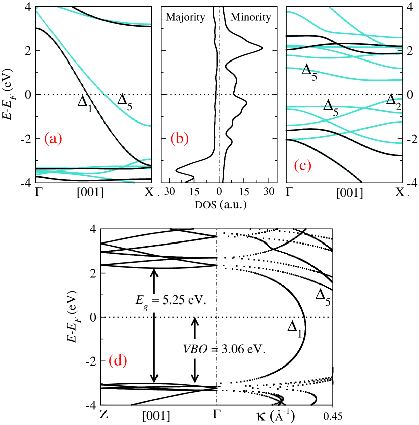
In Figs. 1(a, c) we present the band structure for majority and minority spins along [001] (the proposed stack orientation). As we have seen, BiF3 filters states with symmetry, which are present in Fe3Al only for the majority band. In fact, along the [001] direction (X in -space) at there is a wide band originating from the Al 3 and Fe 4 states in the majority spin channel [Fig. 1(a)], and a band gap in the minority one [Fig. 1(c)]. The first contributions for the minority spin appear at 1.5 eV from , providing a 3 Volt window in which the device is expected to show a large TMR. Note that, as already mentioned, the material is not half-metal as the gap in the minority channel is only along the specific X direction, as shown in Fig. 1(b).
III The all-Heusler FA/BF3/FA spin valve
III.1 Zero bias properties
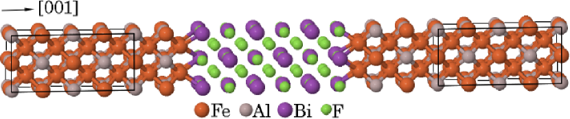
The all-Heusler Fe3Al/BiF3/Fe3Al spin valve is constructed by stacking Fe3Al(001) on BiF3(001), as shown in Fig. 2. Its transport properties are now systematically investigated.
For our transport calculations the in-plane lattice constant is fixed at =5.836 Å, equivalent to the theoretical cubic lattice constant of bulk BiF3. Fixing the in-plane lattice constant induces a small tetragonal distortion in the semi-infinite Fe3Al(001) leads with =1.124 (the cell is relaxed to a forces tolerance of 10 meV/Å). Such a distortion has negligible effects on the electronic structure of the electrodes. The interface energy, corrected for basis set superposition error, is found to be 3.78 J/m2. To put this in context, the computed Fe/MgO interface energy is reported to be 2.52 J/m2 SurfE , namely the Fe3Al/BiF3 interface seems to be stronger than the Fe/MgO one. The Fermi level of the junction is found to lie approximately in the middle of the BiF3 band gap, with a valence band offset of 3.06 eV, as shown in Fig. 1(d).
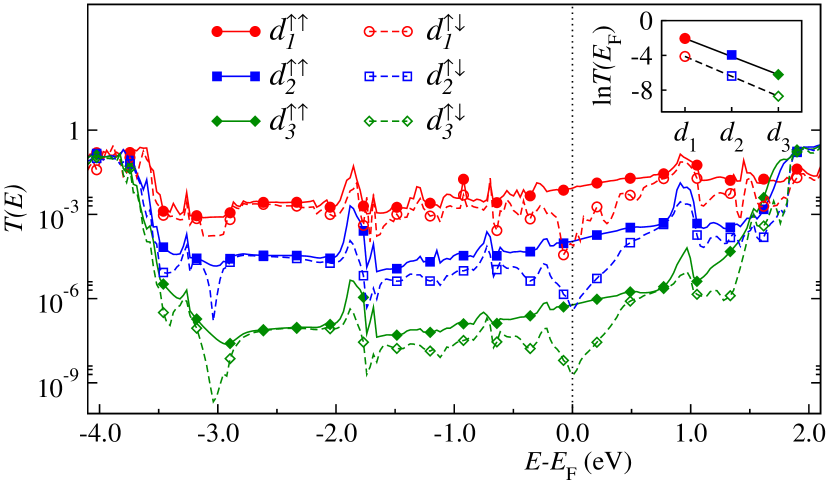
Electronic transport is calculated for three junctions with different BiF3 thicknesses, respectively of 13.10 Å, 18.94 Å and 24.77 Å. The zero-bias transmission coefficients as a function of energy, , are shown in Fig. 3 and clearly demonstrate that there is an exponential reduction of the transmission with the barrier thickness, confirming that the transport mechanism is indeed tunneling with little contribution from possible interface states. For the thinnest junction, 13.10 Å, there is a some structure in for the anti-parallel configuration around . This is the result of the bands not being fully filtered, but it disappears for thicker junctions, for which around is smooth.
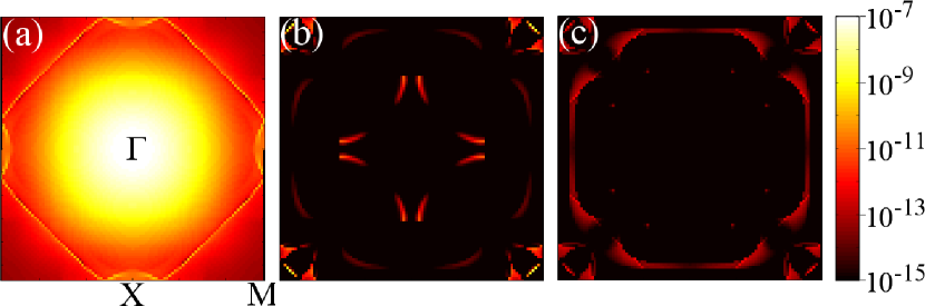
The various transmission coefficients for the [001] direction calculated at the Fermi level are plotted in Fig. 4 as a function of the -vector in the two-dimensional Brillouin zone orthogonal to the transport direction. For the parallel configuration the transmission is dominated by the majority spins and a -region around the -point, while for the minority band and for the anti-parallel configuration the transmission is small and originates from narrow pockets of -vectors away from . This further confirms that the transport is dominated by the symmetry, present only for the majority spins. Importantly, the relative contribution to the total current of the majority spin channel relatively to the minority one in the parallel configuration will exponentially grow as the barrier thickness increases, meaning that for barriers thick enough the Fe3Al/BiF3 system behaves as a half-metal, exactly as Fe/MgO.
III.2 Finite-bias properties
For the 18.94 Å-thick junction we have calculated the current and the TMR as a function of bias [see Fig. 5].
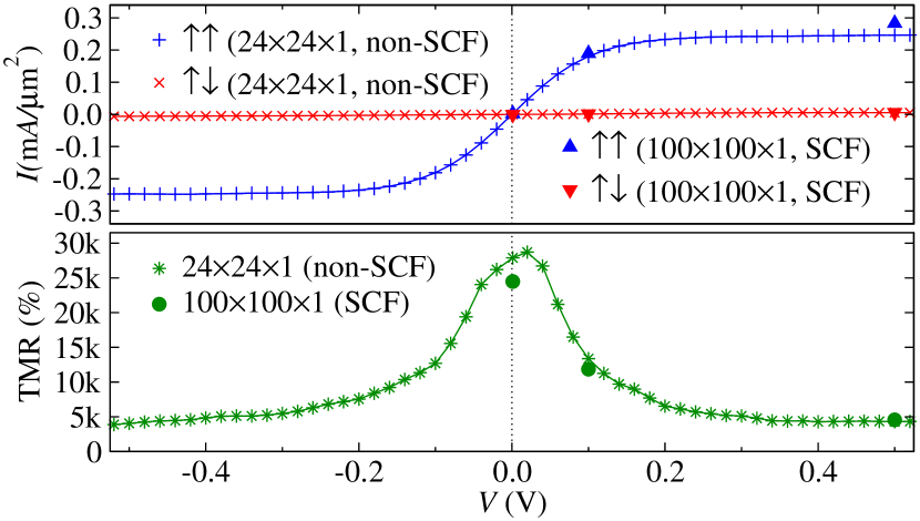
Calculations are performed on a 24241 -point mesh non-self consistently (the potential drop is not self-consistently evaluated, see Nutta ), and have been verified against a 1001001 mesh for a self-consistent calculation at a few selected biases (0, 0.1 and 0.5 Volt). We find that the - characteristic of the parallel configuration is approximately linear at low bias and then saturates at about 0.2 Volt to a value of 0.25 mA/m2. Since the same curve for the anti-parallel configuration is flat and the current is small the TMR as a function of bias decays from the value of 25,000 % to about 5,000% at 0.2 Volt [see below for ]. This is indeed a very encouraging result since an extremely large TMR can be reached for a 2 nm think barrier, and larger values can be obtained by making the barrier thicker. We must note that the theoretical TMR is for the perfect junction and demonstrates that symmetry filtering is the dominant mechanism. The actual TMR of any junction will depend on secondary phases or defects at the interface so the values observed here should be considered an upper limit.
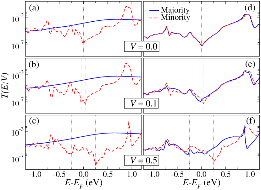
The transmission of the Fe3Al/BiF3/Fe3Al junction has been self-consistently calculated at 0 Volt, 0.1 Volt and 0.5 Volt. In figure 6 we present the transmission coefficient for each bias step, . The behavior of the junction can be understood by considering the filtering of BiF3 and the band structure of the Fe3Al electrodes. We see that when the magnetizations of the electrodes are parallel, for the majority spins is a smooth function of the energy, since the transmission originates from band. At the same time there is no minority spin bands at the Fermi-level along the [001] direction, resulting in a strongly suppressed minority transition around . As the bias voltage increases bands with , and symmetry became available for transport. However, these are filtered by symmetry by the BiF3 barrier and the transmission remains generally small. for the anti-parallel configuration is essentially a convolution of those for the majority and minority spins in the parallel one, i.e. it traces closely the minority spin transmission.
IV Conclusion
In conclusion, we have identified from all known and predicted Heusler alloys a materials combination, which can act as an alternative to the FeCoB/MgO/FeCoB heterostructure. In particular we have looked at the Fe3Al/BiFe3/Fe3Al stack and demonstrated that this junction operates with the same symmetry spin-filtering mechanism of FeCoB/MgO, and as such can display extremely high TMR values. Interestingly, the extended spin-gap along the (100) direction of Fe3Al, gives us a large energy window where to expect a significant TMR. As such for this proposed junction we expect a strong TMR retention at high voltage.
Acknowledgements.
This work was supported by the Higher Education Research Promotion and National Research University Project of Thailand, the Office of the Higher Education Commission, the National Center (NANOTEC), NSTDA, Ministry of Science and Technology, Thailand, through its program of Centers of Excellence Network and by Science Foundation of Ireland (14/IA/2624), and financial support from the European Union’s Horizon 2020 PETMEM and TRANSPIRE projects. The authors wish to acknowledge the SFI/HEA Irish Centre for High-End Computing (ICHEC) and the Trinity Centre for High Performance Computing (TCHPC) for the provision of computational facilities and supports.References
- (1) S. Ikeda, J. Hayakawa, Y. M. Lee, F. Matsukura, Y. Ohno, T. Hanyu, and H. Ohno, IEEE Trans. Electron Devices 54, 991-1002 (2007).
- (2) S. Yuasa, T. Nagahama, A. Fukushima, Y. Suzuki and K. Ando, Nat. Mater. 3, 868-871 (2004).
- (3) S.S.P. Parkin, C. Kaiser, A. Panchula, P. Rice, B. Hughes, M. Samant, and S. Yang, Nat. Mater. 3, 862 (2004).
- (4) W. H. Butler, X.-G. Zhang,T.C. Schulthess and J.M. MacLaren, Phys. Rev. B 63, 054416 (2001).
- (5) J. Mathon and A. Umerski, Phys. Rev. B 63, 220403 (2001).
- (6) A. Hoffmann, and S.D. Bader, Phys. Rev. Appl. 4, 047001 (2015)
- (7) T. Graf, C. Felser and S.S.P. Parkin, Prog. Solid State Chem. 39, 1-50, (2011).
- (8) N. Tezuka, N. Ikeda, F. Mitsuhashi and S. Sugimoto, Appl. Phys. Lett. 94, 162504 (2009)
- (9) W. Wang, E. Liu, M. Kodzuka, H. Sukegawa, M. Wojcik, E. Jedryka, G. H. Wu, K. Inomata, S. Mitani, and K. Hono, Phys. Rev. B 81, 140402(R) (2010).
- (10) S. Tsunegi, Y. Sakuraba, M. Oogane, K. Takanashi, and Y. Ando, Appl. Phys. Lett. 93, 112506 (2008).
- (11) H. X. Liu, Y. Honda, T. Taira, K. I. Matsuda, M. Arita, T. Uemura, and M. Yamamoto, Appl. Phys. Lett. 101, 132418 (2012).
- (12) H. X. Liu, Y. Honda, T. Taira, K. I. Matsuda, M. Arita, T. Uemura, and M. Yamamoto, Appl. Phys. Lett. 101, 132418 (2012).
- (13) R. H. Taylor, F. Rose, C. Toher, O. Levy, K. Yang, M. B. Nardelli, S. Curtarolo, Comp. Mater Sci. 93, 178-192 (2014).
- (14) E. Ozawa, S. Tsunegi, M. Oogane, H. Naganuma, and Y. Ando, J. Phys.: Con. Series 266, 012104 (2011).
- (15) H.X. Liu, Y. Honda, K.I. Matsuda, M. Arita, T. Uemura, and M. Yamamoto, Jpn. J. Appl. Phys. 51, 093004 (2012).
- (16) T. Taira, T. Ishikawa, N. Itabashi, K.I. Matsuda, T. Uemura and M. Yamamoto, J. Phys. D: Appl. Phys. 42, 084015 (2009).
- (17) T. Scheike, H. Sukegawa, T. Furubayashi, Z. Wen, K. Inomata, T. Ohkubo, K. Hono, and S. Mitani, Appl. Phys. Lett. 105, 242407 (2014).
- (18) N. Tezuka, N. Ikeda, S. Sugimoto, and K. Inomata, Appl. Phys. Lett. 89, 252508 (2006).
- (19) Z. Wen, H. Sukegawa, S. Kasai, M. Hayashi, S. Mitani, and K. Inomata, Appl. Phys. Express 5, 063003 (2012).
- (20) N. Tezuka, N. Ikeda, S. Sugimoto, and K. Inomata, Jpn. J. Appl. Phys. 46, L454 (2007).
- (21) N. Tezuka, S. Okamura, A. Miyazaki, M. Kikuchi, and K. Inomata, J. Appl. Phys. 99, 08T314 (2006).
- (22) T. Daibou, M. Shinano, M. Hattori, Y. Sakuraba, M. Oogane, Y. Ando, and T. Miyazaki, IEEE Trans. Magn. 42, 2655 (2006).
- (23) J. Rogge, P. Hedwig, C. Sterwerf, and A. Hütten, IEEE Trans. Magn. 48, 3827 (2012).
- (24) T. Marukame, T. Ishikawa, S. Hakamata, K.I. Matsuda, T. Uemura, and M. Yamamoto, Appl. Phys. Lett. 90, 012508 (2007)
- (25) M Yamamoto, T Marukame, T Ishikawa, K Matsuda, T Uemura and M Arita, J. Phys. D: Appl. Phys. 39, 824-833 (2006).
- (26) T. Marukame, T. Ishikawa, S. Hakamata, K.I. Matsuda, T. Uemura, and M. Yamamoto, IEEE Trans Magn. 43, 2782 (2007).
- (27) T. Kubota, S. Mizukami, Q. L. Ma, H. Naganuma, M. Oogane, Y. Ando, and T. Miyazaki, J. Appl. Phys. 115, 17C704 (2014).
- (28) Y.P. Wang, G.C. Han, H. Lu, J. Qiu, Q.-J. Yap, R. Ji, and K.L. Teo, J. Appl. Phys. 114, 013910 (2013).
- (29) C. Sterwerf, M. Meinert, J. M. Schmalhorst and G. Reiss, IEEE Trans. Magn. 49, 4386 (2013).
- (30) Z. Q. Bai, Y. H. Lu, L. Shen, V. Ko, G. C. Han, and Y. P. Feng, J. Appl. Phys. 111, 093911 (2012).
- (31) K. Nikolaev, P. Kolbo, T. Pokhil, X. P., Y. Chen, T. Ambrose, and O. Mryasov, Appl. Phys. Lett. 94, 222501 (2009).
- (32) Z. Q. Bai, Y.Q. Cai, L. Shen, G.C Han, and Y. P. Feng, Appl. Phys. Lett. 102, 152403 (2013).
- (33) R. H. Taylor, F. Rose, C. Toher, O. Levy, K. Yang, M. B. Nardelli, S. Curtarolo, Comp. Mater Sci. 93, 178-192 (2014).
- (34) C. D. Pemmaraju, T. Archer, D. Sánchez-Portal, and S. Sanvito, Phys. Rev. B 75, 045101 (2007).
- (35) A. Filippetti, C.D. Pemmaraju, S. Sanvito, P. Delugas, D. Puggioni and V. Fiorentini, Phys. Rev. B 84, 195127 (2011).
- (36) J. M. Soler, E. Artacho, J. D. Gale, A. Garcìa, J. Junquera, P. Ordejón, and D. Sánchez-Portal, J. Phys.: Condens Matter 14, 2745-2779 (2002).
- (37) N. Troullier and J. L. Martins, Phys. Rev. B 43, 1993 (1991).
- (38) A. R. Rocha, V. M. Garcìa-Suárez, S. W. Bailey, C. J. Lambert, J. Ferrer and S. Sanvito, Phys. Rev. B 73, 085414 (2006).
- (39) I. Rungger and S. Sanvito, Phys. Rev. B 78, 035407 (2008).
- (40) http://www.materials-mine.com
- (41) U. Croatto, Z. anorg. allg. Chem. 258, 198-204 (1949).
- (42) T. J. Moravec, R. A. Skogman, and E. Bernal G., Appl. Opt. 18, 105-110 (1979).
- (43) K. Kuriyama, K. Nagasawa, and K. Kushida, J. Cryst. Growth, 237-239, 2019 (2002).
- (44) K. Kuriyama, K. Kushida, and R. Taguchi, Solid State Commun. 108, 429 (1998).
- (45) A. Roy, J.W. Bennett, K.M. Rabe, and D. Vanderbilt, Phys. Rev. Latt. 109, 037602 (2012).
- (46) F. Yan, X.W. Zhang, Y.G. Yu, L.P. Yu, A.P. Nagaraja, T. Mason and A. Zunger, Nat. Commun. 6, 7308 (2015).
- (47) N.M. Caffrey, D. Fritsch, T. Archer, S. Sanvito and C. Ederer, Phys. Rev. B 87, 024419 (2013).
- (48) C. Ortiz, O. Eriksson, M. Klintenberg, Comp. Mater Sci. 44, 1042-1049 (2009).
- (49) Z. Yang, X. Wang, L. Liu, S. Yang, X. Su, Comp. Mater Sci. 50, 3131-3138 (2011).
- (50) Z. Yang, X. Wang, Y. Pei, L. Liu and X. Su, Comp. Mater Sci. 60, 212-216 (2012).
- (51) T. J. Burch, K. Raj, P. Jena, J. I. Budnick, V. Niculescu, and W. B. Muir, Phys. Rev. B 19, 2933 (1979)
- (52) T. Gasi, V. Ksenofontov, J. Kiss, S. Chadov, A. K. Nayak, M. Nicklas, J. Winterlik, M. Schwall, P. Klaer, P. Adler, and C. Felser, Phys. Rev. B 87, 064411 (2013).
- (53) L. Hongzhi, Z. Zhiyong, M. Li, X. Shifeng, L. Heyan, Q. Jingping, L. Yangxian and W. Guangheng, J. Phys. D: Appl. Phys. 40, 7121 (2007).
- (54) Y. J. Zhang, W. H. Wang, H. G. Zhang, E. K. Liu, R. S. Ma, G. H. Wu, Physica B 420, 86-89 (2013).
- (55) T. Ryba, Z. Vargova, J. Kovac, P. Diko, V. Kavecansky, S. Piovarci, C. Garcia and R. Varga, IEEE Trans. Magn. 51, 1-3 (2015).
- (56) H. Pandey, P. C. Joshi, R. P. Pant, R. Prasad, S. Auluck, R. C. Budhani, J. Appl. Phys. 111, 023912 (2012).
- (57) M. Belmeguenai, F. Zighem, Y. Roussigné, S.M. Chérif, P. Moch, K. Westerholt, G. Woltersdorf, G. Bayreuther, Phys. Rev. B 79, 024419 (2009).
- (58) P. J. Brown, K.U. Neumann, P. J. Webster, K.R.A. Ziebeck, J. Phys. Condens. Matter 12, 1827 (2000).
- (59) C. Felser and G. H. Fecher, , Springer Netherlands, (2013)
- (60) S. Wurmehl, G.H. Fecher, H.C. Kandpal, V. Ksenofontov, C. Felser, H.J. Lin, J. Morais, Phys. Rev. B 72, 184434 (2005).
- (61) O. Gaier, J. Hamrle, S. Trudel, B. Hillebrands, H. Schneider, and G. Jakob, J. Phys. D: Appl. Phys. 42, 232001 (2009).
- (62) B. Balke, S. Wurmehl, G. H. Fecher, C. Felser, M. C. M.Alves, F. Bernardi, and J. Morais, Appl. Phys. Lett. 90, 172501 (2007).
- (63) O. Gaier, J. Hamrle, S. Trudel, A.C. Parra, B. Hillebrands, C.H.E. Arbelo, M. Jourdan, J. Phys. D: Appl. Phys. 42, 084004 (2009).
- (64) K.H.J. Buschow, P.G. van Engen, R. Jongebreur, J. Magn. Magn. Mater. 38, 1 (1983).
- (65) K. R. Kumar, K. K. Bharathi, J. A. Chelvane, S. Venkatesh, G. Markandeyulu, N. Harishkumar, IEEE Trans. Magn. 45, 3997-3999 (2009).
- (66) X. Q. Chen, R. Podloucky, and P. Rogl, J. Appl. Phys. 100, 113901 (2006).
- (67) C. N. Borca, T. Komesu, H. K. Jeong, P. A. Dowben, D.Ristoiu, Ch. Hordequin, J. P. Noziéres, J. Pierre, S. Stadler and Y. U. Idzerda, Phys. Rev. B. 64, 052409 (2001).
- (68) C. Jiang, M. Venkatesan, J.M.D. Coey, Solid State Com. 118, 513-516 (2001).
- (69) R. Y. Umetsu and T. Kanomata, J. Phys. Proc. 75, 890-897 (2015).
- (70) K. Rode, N. Baadji, D. Betto, Y.-C. Lau, H. Kurt, M. Venkatesan, P. Stamenov, S. Sanvito, J.M.D. Coey, E. Fonda, E. Otero, F. Choueikani, P. Ohresser, F. Porcher and G. André, Phys. Rev. B 87, 184429 (2013).
- (71) D. Orgassa, H. Fujiwara, T.C. Schulthess and W.H. Butler, J. Appl. Phys. 87, 5870 (2000).
- (72) G. D. Samolyuk, B. Ujfalussy, and G. M. Stocks Appl. Phys. Lett. 116, 173908 (2014).
- (73) M. P. Raphael, B. Ravel, Q. Huang, M. A. Willard, S. F. Cheng, B. N. Das, R. M. Stroud, K. M. Bussmann, J. H. Claassen, and V. G. Harris Phys. Rev. B. 66, 104429 (2002).
- (74) D. Wiśnios, A. Kiejna and J. Korecki, Phys. Rev. B 92, 155425 (2015)
- (75) N. Jutong, I. Rungger, C. Schuster, U. Eckern, S. Sanvito and U. Schwingenschlögl, Phys. Rev. B 86, 205310 (2012).