Effect of second order piezoelectricity on excitonic structure of stress-tuned InGaAs/GaAs quantum dots
Abstract
We study the effects of the nonlinear piezoelectricity and the In distribution on the exciton energy, the electron-hole electric dipole moment, and the fine-structure splitting in stress-tunable InGaAs/GaAs quantum dots integrated onto a piezoelectric actuator. In particular, we investigate in detail the contributions of various elements of the expansion of the electrical polarization in terms of externally induced elastic strain on the latter two important quantum dot properties. Based on the comparison of the effects of first- and second-order piezoelectricity we provide a simple relation to estimate the influence of applied anisotropic stress on the quantum dot dipole moment for quantum dots significantly lattice mismatched to the host crystal.
pacs:
78.67.Hc, 73.21.La, 85.35.Be, 77.65.LySemiconductor Quantum dots (QDs) provide a number of appealing applications. Among others, QDs may be used as gain materials for lasers, Bimberg et al. (1997); Ledentsov et al. (2003); Heinrichsdorff et al. (1997) as single photon emitters for optical fibre communication, Huffaker et al. (1998) as building blocks of secure optical links using entangled photon pairs, Trotta et al. (2016) for quantum gates, Křápek et al. (2010); Klenovský et al. (2016) or are used in biomedical applications. Wegner and Hildebrandt (2015)
The capability of QDs to confine the motion of electrons and holes in all three spatial dimensions offers the advantages of a discrete, atom-like electronic system Kastner (1993) within a solid-state platform. The strong confinement and the Coulomb interaction among trapped charge carriers promotes the formation of stable few-particle states Schliwa et al. (2009) like neutral exciton () and biexciton () whose cascaded radiative recombination allows the generation of single- and entangled photons. Michler et al. (2000); Benson et al. (2000) The application of QDs as quantum light sources in advanced quantum communication and computation schemes Senellart et al. (2017); Huber et al. (2018a) demands well-defined transition energies, vanishing fine-structure splitting (FSS) and extensive control over the QDs’ interaction with the charge environment. In this regard, the statistical distribution of structural parameters such as size, shape, or composition of self-assembled QDs Schliwa et al. (2007), which becomes apparent via deviations of essential emission properties among different QDs, represents a major challenge towards application and demands for effective methods for (reversible) post-growth engineering Plumhof et al. (2012) of the electronic structure of individual QDs.
In this context, externally applied stress mediated via piezoelectric actuators Martin-Sanchez et al. (2018) has proven to be an effective tool to (simultaneously) tune transition energies Trotta et al. (2013) and FSS Trotta et al. (2012a, 2016), thus, enabled interference experiments with photons from remote QDs Reindl et al. (2017) or the extraction of high-fidelity polarization-entangled photons. Huber et al. (2018b) In a recent work Aberl et al. (2017) we moreover demonstrated that applied stress allows to control magnitude and alignment of the vertical electron-hole separation in In(Ga)As QDs manifesting itself via a built-in dipole moment () along the growth direction. is commonly present in as-grown QDs Fry et al. (2000) and its interaction with charges in their vicinity leads to spectral diffusion Callsen and Pahn (2015) causing an inhomogeneous linewidth broadening of the corresponding optical transitions and, in turn, degrade the indistinguishability of consecutive photons emitted by QD. It has been found in Ref. [Aberl et al., 2017] that the observed tuning of can only be described by considering nonlinear terms in the expansion of the piezoelectric polarization, the importance of which was first highlighted theoretically by Bester et al.. (Bester et al., 2006a, b) However, that effect is usually difficult to observe experimentally.
In this work we discuss the significance of the second-order piezoelectric terms with regard to the FSS in stress-tuned In(Ga)As QDs. In addition, the previously reported dependences of the transition energy () and on the externally applied stress Aberl et al. (2017) are analyzed in more detail. The experimental data in Ref. [Aberl et al., 2017] were obtained on QDs embedded in n-i-p membrane-diodes bonded on a PMN-PT piezoelectric actuator. This device design allowed to extract and vs. applied stress from micro-photoluminescence (-PL) measurements of the quantum-confined Stark effect (QCSE) Finley et al. (2004) whereas the corresponding FSS was obtained via polarization-resolved -PL measurements of the and spectral lines. The presented theoretical model allows to concurrently reproduce the experimental data for the considered quantities in terms of magnitude and observed stress-dependence. This is achieved while using realistic structural parameters for the investigated QDs and taking into account peculiarities of the used device (-processing) in terms of stress-configuration and prestress. The performed analysis finally allows us to propose an approximate relation of and the externally applied stress applicable to all epitaxial QD systems lattice mismatched with the host material. We want to emphasize that this analysis is not only applicable to type-I QD systems like InGaAs/GaAs, but also for QD systems supporting spatial indirectly located electron and hole states (type-II QDs) that have been reported for distinct III–V material combinations. Klenovský et al. (2015, 2017)
The Taylor expansion of the electrical polarization () in terms of strain () up to second-order terms is , Beya-Wakata et al. (2011) where is the linear term:
| (1) |
and the nonlinear one:
| (2) |
Here are indexed according to the Voigt notation, i.e., , , , , , , Beya-Wakata et al. (2011) where denote the crystallographic axes of the conventional cubic unit cell of the zincblende lattice. Note that even though the third order coefficients of the above expansion were provided by Tse and colleagues, Tse et al. (2013) we restrict ourselves to second-order ones in this work since the magnitude of externally induced (missfit) is of the order 0.1 % (3 %). Aberl et al. (2017) As a consequence, the largest third-order contributions involving the externally induced strain are products of that with the squared misfit strain. These contributions are much smaller than the largest second-order contributions involving the misfit strain in first order.
In the simulations discussed in this work the calculation flow was as follows. First, the geometry of the QD structure was defined on a rectangular grid including the spatially dependent material constituents. Thereafter, the strain field in and around QD was found by minimizing the strain energy. The effect of the resulting strain on the confinement potential was then treated using the Bir-Pikus hamiltonian Bir with positionally dependent parameters. The next step involved the self-consistent solution of single-particle Schrödinger and Poisson equations including the effect of piezoelectric fields up to the second-order in . Note that the single-particle states were obtained within the envelope function method based on 8-band approximation and all the preceding steps of calculation were done using the nextnano simulation suite. Birner et al. (2007) For the full list of material parameters used in this work see Ref. [Sup, a]. Finally, the obtained single-particle states were used as input for the excitonic calculations using the Configuration Interaction (CI) algorithm that we have previously developed. Klenovský et al. (2017) All CI calculations included the computation of direct and exchange Coulomb integrals and were performed with a basis-set of six electron and six hole single-particle states, thus, providing also the effect of correlation.
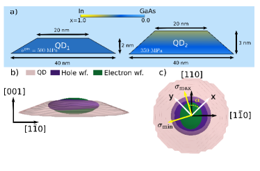 |
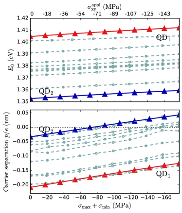
Two InxGa1-xAs/GaAs QDs labeled QD1 and QD2 in Fig. 1 a) were used as model systems. Both have the shape of truncated cones but differ in size and In-Ga alloy distribution. Their parameters were deliberately chosen so that the calculated dependencies of and on the hydrostatic part of the applied anisotropic stress match the experimental results taken from Ref. [Aberl et al., 2017], see Fig. 2. Note, that similarly as in Ref. [Aberl et al., 2017] is considered to be oriented from negative to positive charge throughout this work. The variables and denote the principal stresses Trotta et al. (2015); Sup (b) applied externally by the two-dimensional piezo actuator. In Ref. [Aberl et al., 2017] it was shown that was applied at an angle of with respect to the [100] crystal axis which we adopt also in this work. This stress configuration corresponds to the experimental one as estimated via the measurements of FSS, see supplementary of Ref. [Aberl et al., 2017]. The various coordinate systems used in our model as well as the typical single-particle wavefunctions of electrons and holes are indicated in Fig. 1 b) and c). Note that by assuming a smaller average In concentration (45 % instead of 62.5 %) but a larger In gradient along growth direction (from 25 % to 65 % instead of 45 % to 80 %) as compared to Ref. [Aberl et al., 2017], in this work we could significantly improve the agreement between simulated and measured slope of with applied stress. At the same time, the observed scattering range of energies and dipole moments remains within a model parameter region of comparable width as assumed in Ref. [Aberl et al., 2017].
 |
 |
As discussed in Ref. [Aberl et al., 2017], the bonding of the sample onto the piezo actuator leads to a prestress () independent on the voltage applied to the piezo varying between different dots. As will be discussed towards the end of the paper, only the off-diagonal component of the (symmetric) in-plane prestress tensor effectively affects the electron-hole separation in QDs, where denotes the elementary charge. Consequently, in order to match the measured values of with the results of our calculations we needed to allow for different magnitudes of of 500 and 350 MPa that acted on QD1 and QD2, respectively. We support this assumption by comparing measured values of FSS with those obtained using CI, as discussed in the following.
The effects of on FSS and are different, however, it is possible to estimate a value of such that one can fit both sets of experimental data, i.e., for FSS and . In the top panel of Fig. 3 we show that for QD2 the application of a variable stress leads to a minimal FSS of 1.15 eV for MPa if we assume MPa. Note that by the two scales of the abscissa axes in Fig. 3 together with and the relation Sup (b) all components of the in-plane stress tensor are defined. For larger values of the applied stress leads again to reduction of FSS, but the minimal value of FSS is progressively larger as well as the value of for which the anticrossing occurs. At the same time, the values of for decrease with increasing , see bottom panel of Fig. 3. Interestingly, attains positive values for MPa. However, larger values of lead to negative values of for . Notice that is very similar among different dots. We will return to discussion of this observation later.
It is well known, that apart from FSS also depends on the elongation of the QDs along crystallographic direction. Zielinski (2013); Singh (2018) However, our simulations show that for large QDs with dimensions similar to that of QD2, such elongations in an unrealistically large range between 0.9 and 1.2 cause FSS of less than eV, see Ref. [Sup, c]. Since the elongation-induced FSS is much smaller than the FSS observed in our experiments, it was neglected in our analysis.
Our model reproduces the experimental values of FSS and as well as and reasonably well for MPa indicating that rather large is experienced by our QDs and the value of that is different among dots.
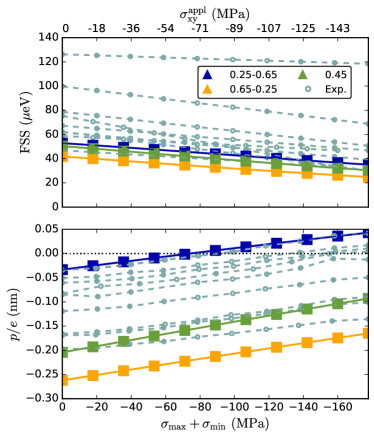 |
Motivated by Refs. [Fry et al., 2000] and [Grundmann et al., 1995] which discussed the influence of indium distribution inside InGaAs/GaAs QDs on , we have tested that observation for our stress-tuned dots. In Fig. 4 we show FSS and as a function of for In contents (i) linearly increasing from 0.25 at the QD base to 0.65 at its apex, (ii) the same but for reverted concentration profile and (iii) for constant In composition of 0.45. Similarly as in Refs. [Fry et al., 2000,Grundmann et al., 1995], we find that at can be varied considerably by changing the slope of In content from nm for (i) to nm for (ii). The case (iii) is found somewhat in between at nm. Note, that the calculated slopes do not fit the experimentally observed ones so well as for different discussed before.
On the other hand, the influence of different In gradients on the values of FSS is much weaker than for . This is expected since FSS is most sensitive to the in-plane QD symmetry Trotta et al. (2015) which is decreased in the presence of in-plane shear stress. Thus, the In gradient cannot be used to explain the spread of values of FSS that we have experimentally observed. Additionally, calculations for different QD height are shown in Ref. [Sup, d].
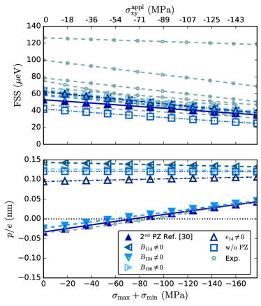
We now proceed with the analysis of the evolution of on and the apparent similarity of its slope among different QDs that we have measured. To investigate the origin of that we have performed calculations in which we have set all piezoelectric parameters equal to zero as well as sequentially , , , and to the values listed in Tab. 1, see Fig. 5.
| InAs | -0.115 | -0.6 | -4.1 | 0.2 |
| GaAs | -0.238 | -0.4 | -3.8 | -0.7 |
Firstly, by comparing the open squares with the full triangles in the top panel of Fig. 5, we note that FSS is dominated by and that the concomitant piezoelectric field as given by Eqs. (1,2) increases FSS by only . As shown by the open triangles, this increase is overestimated twice by considering only. Note that according to Eqs. (1,2) the pre- and applied stress are in-plane and thus result in a purely perpendicular piezoelectric field. As shown in Ref. [Trotta et al., 2012b], electric fields in this direction couple to the FSS only via the different dipole moments of the respective excitons. Obviously, this coupling is less effective for FSS than the in-plane symmetry-breaking effect of . Moreover, the small response of FSS to electric fields in perpendicular direction justifies for our analysis of FSS a posteriori the neglection of the n-i-p diode built-in electric field, which is estimated to be approximately two times smaller than the piezoelectric field.
Secondly, from the bottom panel of Fig. 5 we see from the comparison of the effects of first- and second-order piezo that the latter is dominant for . In particular, the term containing the piezoelectric parameter in Eq. (2) almost exclusively determines the dependencies of on . This is not surprising since the magnitude of is several times larger than that of , , or . Beya-Wakata et al. (2011) This observation, however, suggests a simplification of Eqs. (1) and (2) by discarding all terms except for that for . Let us now expand the element of of the second term in Eq. (2) as
| (3) |
where corresponds to the hydrostatic in-plane strain. The meaning of the other variables is as follows: is the shear strain stemming from the lattice mismatch between the dot material and GaAs matrix, is the shear strain induced by the piezoelectric actuator, and is the fixed shear prestrain; , , and denote the corresponding in-plane hydrostatic components. Variations of the strain fields over the QD volume are neglected, i.e, all strain components represent values averaged over the QD volume.
Since it is reasonable to expect that , we can neglect and arriving at
| (4) |
shedding light to the reason why we see a linear dependence of on in our measurements. In turn, in the presence of large hydrostatic strains typical for QDs lattice mismatched to the host crystal, Eq. (4) has to be used to calculate rather than the commonly used first order expansion given, e.g., in Ref. [YuC, ] which for our case would read
| (5) |
We can now work out the approximate dependence of on as
| (6) |
where ; is a scaling factor that reflects the effect of quantum confinement on position of quasiparticles in QD and is the shear modulus. All built-in dipole moments independent of the piezoelectric polarization (induced, e.g., by a gradient in the In concentration in QDs) are lumped together in . According to Eq. (6), only the off-diagonal element of the prestress tensor is important for the simulation of in highly lattice mismatched QD systems, justifying the inclusion of prestress in our simulations by a single scalar parameter as described in the beginning of the paper.
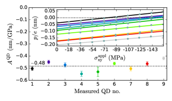
In Fig. 6 we provide the test of Eq. (6) by linear fitting of the experimental dependencies of on . It can be seen that the values for the slope for all studied QDs are scattered by less than around a mean value of nm/GPa. Since is the only experimental parameter in , we conclude that the uncertainty in the value for is due to a variation of of only for our QDs. Finally, the effective offset dipole moment given by Eq. (6) as pronouncedly varies by for the QDs shown in Fig. 6 as a consequence of variations of and . To which extent each of them contributes to the observed variation of cannot be concluded based on the experimental data available. Finally, by comparing the effects of Eqs. (4) and (5) on , respectively, using Eq. (6) we find that the former provides times larger values of than the latter.
In conclusion, we have studied the effects of nonlinear piezoelectricity on built-in electric dipole and excitonic fine-structure splitting energy in stress-tuned InGaAs/GaAs quantum dots and pinpointed its importance as compared to first-order terms only. Furthermore, it was found that while the dipole is influenced by the shear prestress via the piezoelectric effect, the latter effect is relatively unimportant for fine-structure splitting. On the contrary, shear prestress influences fine-structure by reducing the dot overall symmetry, particularly in the base plane of InGaAs/GaAs quantum dots. Finally, we have found the dominant piezoelectric term and provided an approximate relation to estimate the influence of the applied stress on the electrical dipole moment for the InGaAs/GaAs QD system. The applicability of our simplified model extends also to other strongly lattice mismatched piezoelectric QD systems with large built-in hydrostatic strains. Its contribution to potentially dominates the more commonly used relation . Noticeably, in the case of InGaAs/GaAs quantum dots studied in this work our model led to almost an order of magnitude larger effect of applied shear stress on quantum dot dipole than that when only the linear piezoelectricity was considered.
P.K. would like to thank Prof. Dieter Bimberg for fruitful discussions. A part of the work was carried out under the project CEITEC 2020 (LQ1601) with financial support from the Ministry of Education, Youth and Sports of the Czech Republic under the National Sustainability Programme II. The authors P.K., P.S., T.F., A.R., and R.T. were supported through the project MOBILITY jointly funded by the Ministry of Education, Youth and Sports of the Czech Republic under code 7AMB17AT044 and by the Austrian Federal Ministry of Science, Research and Economy under the OEAD project CZ 07/2017. A.R. acknowledges financial support of the Austrian Science Fund (FWF): P 29603. Part of this work is financially supported by the European Research council (ERC) under the European Union’s Horizon 2020 Research and Innovation Programme (SPQRel, Grant Agreement No. 679183).
References
- Bimberg et al. (1997) D. Bimberg, N. Kirstaedter, N. N. Ledentsov, Z. I. Alferov, P. S. Kopev, and V. M. Ustinov, Ieee Journal of Selected Topics in Quantum Electronics 3, 196 (1997).
- Ledentsov et al. (2003) N. Ledentsov, A. Kovsh, A. Zhukov, N. Maleev, S. Mikhrin, A. Vasil’ev, E. Sernenova, M. Maximov, Y. Shernyakov, N. Kryzhanovskaya, V. Ustinov, and D. Bimberg, Electron. Lett. 39, 1126 (2003).
- Heinrichsdorff et al. (1997) F. Heinrichsdorff, M. H. Mao, N. Kirstaedter, A. Krost, D. Bimberg, A. O. Kosogov, and P. Werner, Applied Physics Letters 71, 22 (1997).
- Huffaker et al. (1998) D. L. Huffaker, G. Park, Z. Zou, O. B. Shchekin, and D. G. Deppe, Applied Physics Letters 73, 2564 (1998).
- Trotta et al. (2016) R. Trotta, J. Martín-Sánchez, J. S. Wildmann, G. Piredda, M. Reindl, C. Schimpf, E. Zallo, S. Stroj, J. Edlinger, and A. Rastelli, Nature Comm. 7, 10375 (2016).
- Křápek et al. (2010) V. Křápek, P. Klenovský, A. Rastelli, O. G. Schmidt, and D. Munzar, Quantum Dots 2010 245, 012027 (2010).
- Klenovský et al. (2016) P. Klenovský, V. Křápek, and J. Humlíček, Acta Physica Polonica A 129, A62 (2016).
- Wegner and Hildebrandt (2015) K. D. Wegner and N. Hildebrandt, Chemical Society Reviews 44, 4792 (2015).
- Kastner (1993) M. A. Kastner, Physics today 46, 24 (1993).
- Schliwa et al. (2009) A. Schliwa, M. Winkelnkemper, and D. Bimberg, Phys. Rev. B 79, 075443 (2009).
- Michler et al. (2000) P. Michler, A. Kiraz, C. Becher, W. Schoenfeld, P. Petroff, L. Zhang, E. Hu, and A. Imamoglu, science 290, 2282 (2000).
- Benson et al. (2000) O. Benson, C. Santori, M. Pelton, and Y. Yamamoto, Phys. Rev. Lett. 84, 2513 (2000).
- Senellart et al. (2017) P. Senellart, G. Solomon, and A. White, Nature nanotechnology 12, 1026 (2017).
- Huber et al. (2018a) D. Huber, M. Reindl, J. Aberl, A. Rastelli, and R. Trotta, arXiv preprint arXiv:1804.10472 (2018a).
- Schliwa et al. (2007) A. Schliwa, M. Winkelnkemper, and D. Bimberg, Phys. Rev. B 76, 205324 (2007).
- Plumhof et al. (2012) J. D. Plumhof, R. Trotta, A. Rastelli, and O. G. Schmidt, Nanoscale Research Letters 7, 336 (2012).
- Martin-Sanchez et al. (2018) J. Martin-Sanchez, R. Trotta, A. Mariscal, R. Serna, G. Piredda, S. Stroj, J. Edlinger, C. Schimpf, J. Aberl, T. Lettner, J. Wildmann, H. Huang, X. Yuan, D. Ziss, J. Stangl, and A. Rastelli, Semiconductor Science and Technology 33, 013001 (2018).
- Trotta et al. (2013) R. Trotta, E. Zallo, E. Magerl, O. G. Schmidt, and A. Rastelli, Phys. Rev. B 88, 155312 (2013).
- Trotta et al. (2012a) R. Trotta, E. Zallo, C. Ortix, P. Atkinson, J. D. Plumhof, J. van den Brink, A. Rastelli, and O. G. Schmidt, Phys. Rev. Lett. 109, 147401 (2012a).
- Reindl et al. (2017) M. Reindl, K. D. Jöns, D. Huber, C. Schimpf, Y. Huo, V. Zwiller, A. Rastelli, and R. Trotta, Nano Letters 17, 4090 (2017).
- Huber et al. (2018b) D. Huber, M. Reindl, S. F. C. da Silva, C. Schimpf, J. Martin-Sanchez, G. Piredda, J. Edlinger, A. Rastelli, and R. Trotta, arXiv preprint arXiv:1801.06655 (2018b).
- Aberl et al. (2017) J. Aberl, P. Klenovský, J. S. Wildmann, J. Martín-Sánchez, T. Fromherz, E. Zallo, J. Humlíček, A. Rastelli, and R. Trotta, Phys. Rev. B 70, 201308 (2017).
- Fry et al. (2000) P. W. Fry, I. E. Itskevich, D. J. Mowbray, M. S. Skolnick, J. J. Finley, J. A. Barker, E. P. O’Reilly, L. R. Wilson, I. A. Larkin, P. A. Maksym, M. Hopkinson, M. Al-Khafaji, J. P. R. David, A. G. Cullis, G. Hill, and J. C. Clark, Phys. Rev. Lett. 84, 733 (2000).
- Callsen and Pahn (2015) G. Callsen and G. M. O. Pahn, physica status solidi (RRL) Rapid Research Letters 9, 521 (2015).
- Bester et al. (2006a) G. Bester, X. Wu, D. Vanderbilt, and A. Zunger, Phys. Rev. Lett. 96, 187602 (2006a).
- Bester et al. (2006b) G. Bester, A. Zunger, X. Wu, and D. Vanderbilt, Phys. Rev. B 74, 081305 (2006b).
- Finley et al. (2004) J. J. Finley, M. Sabathil, P. Vogl, G. Abstreiter, R. Oulton, A. I. Tartakovskii, D. J. Mowbray, M. S. Skolnick, S. L. Liew, A. G. Cullis, and M. Hopkinson, Phys. Rev. B 70, 201308 (2004).
- Klenovský et al. (2015) P. Klenovský, D. Hemzal, P. Steindl, M. Zíková, V. Křápek, and J. Humlíček, Physical Review B 92, 241302 (2015).
- Klenovský et al. (2017) P. Klenovský, P. Steindl, and D. Geffroy, Scientific Reports 7, 45568 (2017).
- Beya-Wakata et al. (2011) A. Beya-Wakata, P. Y. Prodhomme, and G. Bester, Physical Review B 84, 195207 (2011).
- Tse et al. (2013) G. Tse, J. Pal, U. Monteverde, R. Garg, V. Haxha, M. A. Migliorato, and S. Tomic, Journal of Applied Physics 114, 073515 (2013).
- (32) G. L. Bir, G. E. Pikus, Symmetry and Strain-Induced Effects in Semiconductors (Wiley, New York, 1974).
- Birner et al. (2007) S. Birner, T. Zibold, T. Andlauer, T. Kubis, M. Sabathil, A. Trellakis, and P. Vogl, IEEE Trans. El. Dev. 54, 2137 (2007).
- Sup (a) See Supplemental Material at [URL will be inserted by publisher] for section SIV showing the values of the material parameters used in the calculations. (a).
- Trotta et al. (2015) R. Trotta, J. Martín-Sánchez, I. Daruka, C. Ortix, and A. Rastelli, Phys. Rev. Lett. 114, 150502 (2015).
- Sup (b) See Supplemental Material at [URL will be inserted by publisher] for section SI describing the derivation of the correspondence between stress in principal and Cartesian coordinates. (b).
- Zielinski (2013) M. Zielinski, Physical Review B 88, 155319 (2013).
- Singh (2018) R. Singh, Journal of Luminescence (2018).
- Sup (c) See Supplemental Material at [URL will be inserted by publisher] for Fig. S1 where are calculations for different elongation of QD2. (c).
- Grundmann et al. (1995) M. Grundmann, O. Stier, and D. Bimberg, Phys. Rev. B 52, 11969 (1995).
- Sup (d) See Supplemental Material at [URL will be inserted by publisher] for Fig. S2 where are calculations for different QD height. (d).
- Trotta et al. (2012b) R. Trotta, P. Atkinson, J. D. Plumhof, E. Zallo, R. O. Rezaev, S. Kumar, S. Baunack, J. R. Schröter, A. Rastelli, and O. G. Schmidt, Advanced Materials 24, 2668 (2012b).
- (43) P.Y. Yu, M. Cardona, Fundamentals of Semiconductors (Springer, Berlin, 2001).