Critical-point model dielectric function analysis of WO3 thin films deposited by atomic layer deposition techniques
Abstract
WO3 thin films were grown by atomic layer deposition and spectroscopic ellipsometry data gathered in the photon energy range of 0.72-8.5 eV and from multiple samples was utilized to determine the frequency dependent complex-valued isotropic dielectric function for WO3. We employ a critical-point model dielectric function analysis and determine a parameterized set of oscillators and compare the observed critical-point contributions with the vertical transition energy distribution found within the band structure of WO3 calculated by density functional theory. We investigate surface roughness with atomic force microscopy and compare to ellipsometric determined effective roughness layer thickness.
I Introduction
Transition-metal oxides such as tungsten tri-oxide (WO3) continue to receive increasing interest due to their potential for use in photovoltaics,Ou et al. (2013) chemical gas sensing,Zhuiykov (2008); Kim et al. (2015) electrochromic smart windows,Lee et al. (2006) and optical switchingGranqvist (2000) applications, for example. Physical vapor deposition (PVD) processes such as sputteringSberveglieri et al. (1995); Depero et al. (1996); Moulzolf, Ding, and Lad (2001) and thermal evaporation techniquesLee et al. (2000); Cantalini et al. (1996) and chemical vapor deposition (CVD) processesCross and Parkin (2003); Chakrapani et al. (2016) are convenient to fabricate WO3 thin films. It has been reported that the electrical, optical, and photocatalytic properties of WO3 thin films depend crucially on the growth conditions.Zhuiykov and Kats (2013); Liu et al. (2015); Labidi et al. (2005); Ping, Rocca, and Galli (2013); Liu et al. (2011); Zheng et al. (2015) For example, Subrahmanyam et al. examined the effects of the growth conditions during a sputtering process onto the optical and structural properties of WO3 thin films.Subrahmanyam and Karuppasamy (2007) Hao et al. employed a spray pyrolysis method in order to fabricate WO3 thin films, and investigated changes of their transient photoconductivity properties upon thermal annealing.Hao, Studenikin, and Cocivera (2001) Gullapalli et al. studied sputter-deposited nanocrystalline WO3 films, and determined their transmittance and reflectance within the range of 1 eV–4.2 eV.Gullapalli, Vemuri, and Ramana (2010) Saenger et al. deposited amorphous WO3 thin films by magnetron sputtering, and studied their polaron and phonon properties upon reversible electrochemical proton intercalation and reported the dielectric function in the spectral range of 0.037–3.34 eV.Saenger et al. (2008). The dielectric function can provide insight into optical and electrical properties of a materialXiong, Wang, and Chang (1993); Li et al. (2014) and has been investigated previously for WO3 using several methods including ellipsometric techniques. For example, K. von Rottkay et al. utilized ellipsometry and spectrophotometry to investigate the optical constants within the range 0.49 eV–4.13 eV of electrochromic tungsten oxide on ITO coated glass by e-beam evaporation.Von Rottkay, Rubin, and Wen (1997) I.Valyukh et al. fabricated tungsten oxide films by reactive DC magnetron sputtering and performed ellipsometric data analysis based transmittance and reflectance measurements from 0.72 eV–4.13 eV.Valyukh et al. (2010) A. Georg et al. studied WOx films with varying crystallinity grown by thermal evaporation comparing optical constants within the range from 0.62 eV–3.72 eV. Georg, Graf, and Wittwer (1998) D. H. Mendelsohn et al., reported on the refractive index and extinction coefficient using ellipsometry in the spectral range 0.5 eV–3.5 eV of polycrystalline electrochromic WO3 films, grown by RF sputtering.Mendelsohn and Goldner (1984) However, to the best of our knowledge, a wide spectral range including ultraviolet to vacuum ultraviolet dielectric function were not yet reported for WO3 thin films using ellipsometry.
Spectroscopic ellipsometry (SE) is a convenient non-destructive, non-contact optical characterization method, which has been widely employed to study thin films.Rothen (1945, 1945); Schmidt, Schubert, and Schubert (2012); Knaut et al. (2012); Järrendahl and Arwin (1998); Schubert (1998); Schmidt, Schubert, and Schubert (2008) The interaction between an incident polarized light beam and a stack of layered materials of interest with plane parallel interfaces results in change in the polarization of the reflected or transmitted light beam.Fujiwara (2007) The complex-valued ratio, , taken between incident and reflected or transmitted electric field components of a monochromatic electromagnetic plane waves can be accurately measured in terms of the amplitude ratio, , and the phase difference, . For isotropic materials and for the case of reflection geometry the relation holds
| (1) |
where and are the Fresnel reflection coefficients for parallel and perpendicular polarized light, respectively.Fujiwara (2007); Schubert (2004)
In order to resolve both thickness and the complex-valued frequency dependent dielectric function of a thin film, a multiple sample analysis approach is necessary.Tompkins et al. (2000); Koster and Rijnders (2011); Hilfiker et al. (2008) In this method, the dielectric function can be obtained without use of physical model lineshape functions using a wavelength-by-wavelength analysis where data points at the same photon energy (wavelength) from multiple samples are simultaneously analyzed fitting for thicknesses as well as the real and imaginary part of the dielectric function.Järrendahl and Arwin (1998) The necessary requirement for this method is that the dielectric functions of the material of interest in the thin film samples are identical. A second requirement is that the samples differ significantly in their thickness. This scheme can be extended to more complex sample structures, for example, by incorporation of the effects of surface and interface roughness, and by including additional model parameters such as model roughness layer thickness and porosity.Heinemeyer et al. (2008); Easwarakhanthan et al. (2007)
The optical properties of an effective roughness layer can be calculated using an effective medium approximation which adds together the dielectric function of the material and air with a 50:50 ratio.Fujiwara (2007) By integrating the model roughness layer, the optical effect of a rough surface onto the ellipsometric spectra is successfully modeled. It has been demonstrated that the approach of the effective surface roughness model layer predicts accurately the mean square roughness of physically rough surfaces for very small roughness parameters against the wavelength.Fang et al. (1997); Petrik et al. (1998)
The electronic band-to-band transitions give rise to critical-point (CP) features in the dielectric function. A model dielectric function (MDF) approach can be formulated using physically meaningful lineshape functions with model parameters determined by a MDF analysis.Adachi, Kimura, and Suzuki (1993) In this work, CP contributions to the WO3 dielectric function are identified and modeled with a 3D-M1 Adachi function for the first CP and Gaussian broadened oscillators for higher energy features. The M1 Adachi function is given by:Adachi, Kimura, and Suzuki (1993)
| (2) |
where with , , and are CP amplitude, transition energy, and broadening parameters, respectively. The Gaussian oscillator used for higher energy features is given by:Mock et al. (2016)
| (3) |
where with , , and are CP amplitude, center transition energy, and broadening parameters, respectively. The real part, , is then obtained from Kramers-Kronig integrationMeneses, Malki, and Echegut (2006); Mock et al. (2016)
| (4) |
In this study, we employ SE to characterize the optical properties of the WO3 thin films. We utilize analysis of multiple samples using different thickness of WO3 in order to determine the isotropic dielectric function without model lineshape assumptions. Valyukh et al. (2010) Three films are deposited using an atomic layer deposition technique for , , and cycles under the same deposition conditions. SE data is collected and analyzed in the spectral range from eV at multiple angles of incidence. We therefore determine the dielectric function of the as-grown WO3 as well as thicknesses and effective roughness thicknesses of each film. Atomic force microscopy (AFM) measurements are performed and resulting roughness is with the effective roughness parameter found in the SE analysis. We compare results from our critical point analysis of the as-deposited WO3 films to the envelope of expected the band-to-band transitions calculated using density functional theory.
II Experimental Details
Thin films of WO3 were deposited on silicon wafers by plasma-enhanced ALD (Fiji F200, Veeco CNT). The oriented wafers with native oxide were cut from low-doped, p-type conductive, single crystalline silicon. After sample insertion into the reactor, and prior to the main deposition processes, a 300 W oxygen plasma was applied for sec in order to remove residual surface contaminants. Subsequently, a stabilization period was implemented to let the sample reach a steady state temperature. ALD techniques using cyclic exposure to (tBuN)2(Me2N)2W, H2O, and oxygen plasma as described in Ref. Liu et al., 2011.
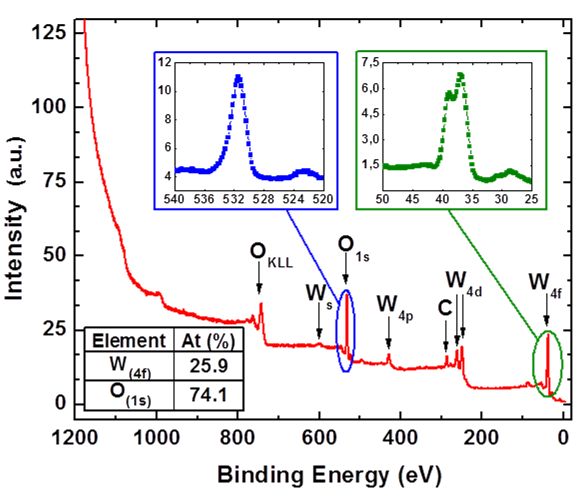
In order to determine elemental and compositional information of our fabricated samples, X-ray photoelectron spectroscopy (XPS) is utilized. The resulting XPS survey spectra corresponding to the samples fabricated with 150 ALD cycles is presented in Fig. 1. The insets of Fig.1 show the spectra for O(1s) and W(4f) core levels. We find that only oxygen and tungsten are present in the film, with a chemical composition of 74.1% and 25.9%, respectively. These values are in good agreement with what is expected for WO3 films.
SE measurements were conducted in the spectral range of 0.72–6.2 eV using a dual rotating compensator ellipsometer (RC2, J.A. Woollam Co., Inc.), and in the spectral range of 4–8.5 eV using a rotating analyzer ellipsometer with an automated compensator (VUV-VASE, J.A. Woollam Co., Inc.). All spectra were collected at angles of incidence of 45∘, 55∘, 65∘, and 75∘. All ellipsometric spectra were analyzed using ellipsometry data modeling software (WVASE32, J.A. Woollam Co., Inc.).
AFM images were collected from all samples using a multi-mode atomic force microscope (Bruker-Nanoscope III). For all measurements, the field size was chosen to be 22 m with a line resolution of 512512. The AFM scans were performed in tapping mode with a scan velocity of 0.1 lines per second. Image data were analyzed using Nanoscope Visualization and Analysis software. The model surface roughness parameters of the investigated samples were calculated from the image data, and obtained as Rq, the average of height deviation taken from the mean image data plane, and as Ra, the arithmetic average of the absolute values of the surface height deviations measured from the mean geometric (flat) surface plane.Oraby and Alaskari (2010)
A density functional theory approach was used for bandstructure calculations. The calculations were performed using the plane-wave density functional theory (DFT) code Quantum ESPRESSO. [QuantumESPRESSOisavailablefromhttp://www.quantum-espresso.org.Seealso:]GiannozziJPCM2009QE Atomic coordinates and unit cell parameters were taken from Ref. Woodward, Sleight, and Vogt, 1995. We used the exchange-correlation functional of Perdew and Zunger Perdew and Zunger (1981) and the atoms were represented by Optimized Norm-Conserving Vanderbilt (ONCV) scalar-relativistic pseudopotentials,Hamann (2013) which we generated for the PZ functional using the code ONCVPSPONC with the optimized parameters of the SG15 distribution of pseudopotentials.Schlipf and Gygi (2015) The simple monoclinic unit cell containing 8 tungsten atoms and 24 oxygen atoms was first relaxed to force levels less than 10-4 Ry/Bohr. A regular shifted 222 Monkhorst-Pack grid was used for sampling of the Brillouin Zone.Monkhorst and Pack (1976) A convergence threshold of 110-11 was used to reach self consistency with a large electronic wavefunction cut-off of 100 Ry. For the relaxed structure an additional non-scf calculation was performed on a non-shifted (-centered) 222 grid, with additional 40 unoccupied bands and somewhat relaxed convergence criteria of 110-9.
The allowed band-to-band transitions were identified by analyzing the matrix elements of the momentum operator between conduction and valence bands at the point (Figure 5). Only the transitions with significant values of the matrix elements were considered, i.e., transitions with 0.05 were discarded. Also, due to the fact that DFT underestimates the energy gap between occupied and unoccupied states a rigid shift of energy was applied, i.e., the energy of all the transitions were shifted by 2.01 eV, the value chosen to match the lowest vertical transition with first CP experimentally determined in this work.
III Results and Discussion
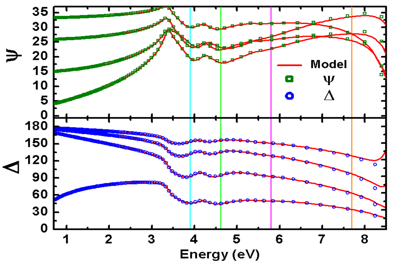
Spectroscopic ellipsometric data, and from a WO3 thin film fabricated with 150 ALD cycles on silicon substrate are presented in Fig. 2 along with the corresponding best match model calculations from the multiple sample analysis. Similar data was obtained for each of the fabricated samples allowing for the extraction of the dielectric function.
| Thickness (nm) | Sample I | Sample II | Sample III |
|---|---|---|---|
| (75 cycles) | (110 cycles) | (150 cycles) | |
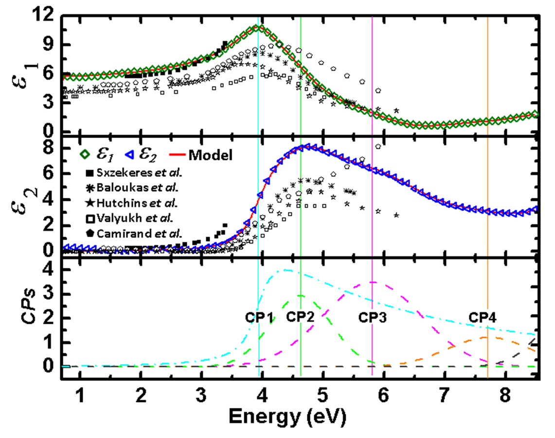
The WO3 layer thicknesses of the investigated samples determined by this MSA approach are presented in Table 1. The real and imaginary parts of the spectrally dependent dielectric function, and , determined using a wavelength-by-wavelength regression analysis and are shown as green squares in Fig. 3 together with dielectric function data from selected literature are reproduced with permission from references Szekeres, Gogova, and Gesheva, 1999; Camirand et al., 2015; Valyukh et al., 2010; Baloukas and Martinu, 2012; Hutchins et al., 2006. We find that optical constants are highly dependent on the deposition conditions. Additionally, surface roughness plays a large part in the determination of optical constants in the visible-vacuum ultraviolet spectral region of thin films. Tompkins and Hilfiker (2005) Many of the previous studies onto the dielectric function of WO3 thin films did not take the surface roughness into accountGarde (2016); Baloukas and Martinu (2012); Hutchins et al. (2006); Szekeres, Gogova, and Gesheva (1999); Ping, Rocca, and Galli (2013); Sun et al. (2004), which could explain some of the variation seen in Fig. 3.
| Fabrication | Method | Egap (eV) | |
|---|---|---|---|
| Our work | ALD | Spectroscopic | |
| ellipsometry | |||
| Ref. Valyukh et al.,2010 | reactive DC | Spectroscopic | 3.15 |
| magnetron sputtering | ellipsometry | ||
| Ref. Szekeres, Gogova, and Gesheva,1999 | CVD | Absorption | 3.25-3.4 |
| spectra | |||
| Ref. Hutchins et al.,2006 | Thermal | Spectrophotometric | |
| evaporation | transmissivity | ||
| Ref. Baloukas and Martinu,2012 | Reactive RF | Spectroscopic | |
| magnetron sputtering | ellipsometry | ||
| Ref. Madhavi et al.,2014 | Reactive RF | Optical | 3.08-3.48 |
| magnetron sputtering | transmittance | ||
| Ref. Garde,2016 | Vacuum | Absorption | 3.9 |
| evaporation | spectra | ||
| Ref. Ping, Rocca, and Galli,2013 | - | DFT Calculations | 3.26111 G0W0 band gap calculations of -WO3 are performed by considering the experimental geometry. |
| Ref. Sun et al.,2004 | - | DFT Calculations | 3.46222This is the energy gap of (WO3)n where cluster. |
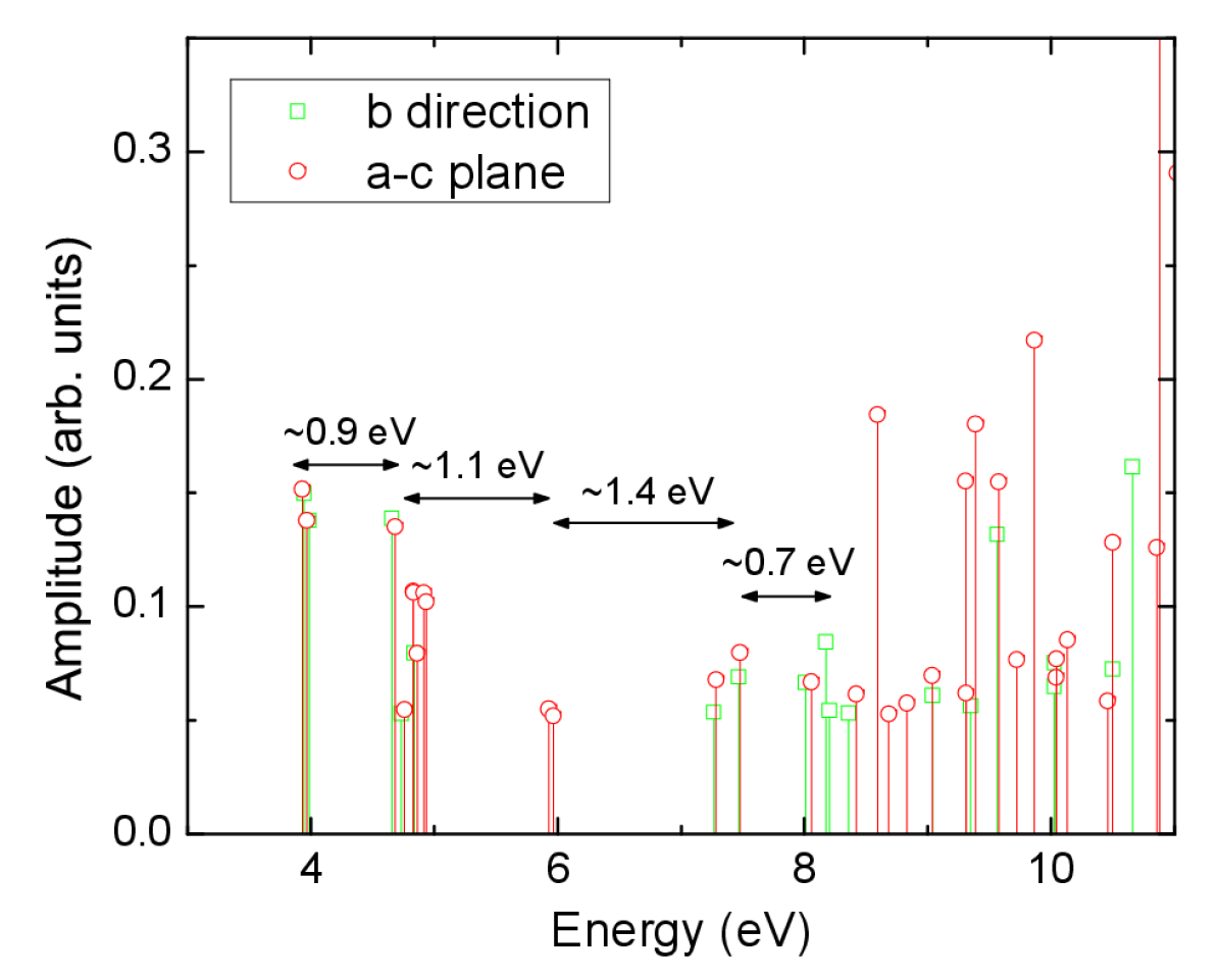
Five line-functions were fit to the experimentally obtained dielectric constants. A single Adachi M1 function (eq. 2) was used to render the shape from the lowest critical point feature and four Gaussian functions (eq. 3) were used to model higher energy transitions.
The resulting dielectric function lineshapes from the critical point analysis are shown in Fig. 3 as red solid lines. Individual contributions to the dielectric function are shown in . Vertical lines at the determined center energies in both Figs. 2 and 3. Best match model parameters for CP analysis lineshape functions are presented in Table 3.
The wide variation in reported band gap energy can also be attributed to variation in deposition methods and conditions with vacuum evaporation seeming to yield the widest band gap. The energy band gap values of selected tungsten oxide thin films which are deposited and optically characterized by different methods are listed in Table 2. Unlike the other studies Garde (2016); Szekeres, Gogova, and Gesheva (1999), in this report, having extended spectral range unraveled four higher energy CPs in the dielectric function of our ALD fabricated WO3 ultra thin films.
| Critical Point Analysis | |||||
| Parameter | CP1333CP1 modeled by Adachi function (CPM1), Eq.2. | CP2444CP2, CP3, and CP4, CP5 modeled by Gaussian functions, Eq.3 and Eq.4. | CP3 | CP4 | CP5555Transition outside investigated region determined with limited sensitivity. |
| (eV) | |||||
| (eV) | |||||
| (eV) | |||||
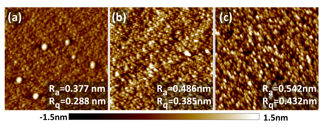
Increased thickness of the optical effective roughness layer is observed with increased WO3 thin film thickness with determined values given in Table 1. An increase of approximately 160% is observed between the samples with 75 and 150 ALD cycles. A similar trend is observed in measured surface roughness obtained from AFM image analysis shown in Fig. 4. The values for Ra and Rq are inlaid for each corresponding sample. An increase of approximately 140% is seen in the Ra average and approximately 150% in the Rq average between the samples with 75 and 150 ALD cycles showing excellent agreement with ellipsometric results.
A snapshot of allowed optical transitions in WO3 was calculated for the most common, monoclinic form of WO3 and is shown in Fig. 5. All significant allowed transitions regardless of symmetry are plotted. Transitions are observed to fall into several clusters which are spaced in a similar way to the identified broad CP transitions from the ellipsometric analysis.
IV CONCLUSIONS
Deposition of WO3 by ALD was performed and spectroscopic ellipsometry was utilized to determine optical properties of the thin films. WO3 thin films with various thicknesses (6.57 nm, 10.52 nm, and 14.51 nm for 75, 110, and 150 cycles, respectively) were investigated using a multiple sample analysis which allowed the thicknesses and optical properties to be decoupled. A comprehensive optical characterization using a critical point analysis was conducted in the wide spectral range of - eV and compared with density functional theory calculations. Energetic locations for clusters of DFT calculated allowed transitions agree well with ellipsometric determined energy parameters of critical point features in the dielectric function.
V Acknowledgements
This work was supported in part by the National Science Foundation (NSF) through the Center for Nanohybrid Functional Materials (EPS-1004094), the Nebraska Materials Research Science and Engineering Center (MRSEC) (DMR-1420645) and awards CMMI 1337856 and EAR 1521428. The authors further acknowledge financial support by the University of Nebraska-Lincoln, the J. A. Woollam Co., Inc., and the J. A. Woollam Foundation.
VI References
References
- Ou et al. (2013) J. Z. Ou, R. A. Rani, S. Balendhran, A. S. Zoolfakar, M. R. Field, S. Zhuiykov, A. P. O’Mullane, and K. Kalantar-zadeh, Electrochem. Commun. 27, 128 (2013).
- Zhuiykov (2008) S. Zhuiykov, Electrochem. Commun. 10, 839 (2008).
- Kim et al. (2015) S. Kim, S. Park, S. Park, and C. Lee, Sens. Actuators, B 209, 180 (2015).
- Lee et al. (2006) S.-H. Lee, R. Deshpande, P. A. Parilla, K. M. Jones, B. To, A. H. Mahan, and A. C. Dillon, Adv. Mater. 18, 763 (2006).
- Granqvist (2000) C. G. Granqvist, Sol. Energy Mater. Sol. Cells 60, 201 (2000).
- Sberveglieri et al. (1995) G. Sberveglieri, L. Depero, S. Groppelli, and P. Nelli, Sens. Actuators, B 26, 89 (1995).
- Depero et al. (1996) L. Depero, S. Groppelli, I. Natali-Sora, L. Sangaletti, G. Sberveglieri, and E. Tondello, J. Solid State Chem. 121, 379 (1996).
- Moulzolf, Ding, and Lad (2001) S. C. Moulzolf, S.-a. Ding, and R. J. Lad, Sens. Actuators, B 77, 375 (2001).
- Lee et al. (2000) D.-S. Lee, J.-W. Lim, S.-M. Lee, J.-S. Huh, and D.-D. Lee, Sens. Actuators, B 64, 31 (2000).
- Cantalini et al. (1996) C. Cantalini, H. Sun, M. Faccio, M. Pelino, S. Santucci, L. Lozzi, and M. Passacantando, Sens. Actuators, B 31, 81 (1996).
- Cross and Parkin (2003) W. B. Cross and I. P. Parkin, Chem. Commun. 14, 1696 (2003).
- Chakrapani et al. (2016) V. Chakrapani, M. Brier, A. Puntambekar, and T. DiGiovanni, J. Mater. Res. 31, 17 (2016).
- Zhuiykov and Kats (2013) S. Zhuiykov and E. Kats, Ionics 19, 825 (2013).
- Liu et al. (2015) J. Liu, M. Zhong, J. Li, A. Pan, and X. Zhu, Mater. Lett. 148, 184 (2015).
- Labidi et al. (2005) A. Labidi, C. Jacolin, M. Bendahan, A. Abdelghani, J. Guerin, K. Aguir, and M. Maaref, Sens. Actuators, B 106, 713 (2005).
- Ping, Rocca, and Galli (2013) Y. Ping, D. Rocca, and G. Galli, Phy. Rev. B 87, 165203 (2013).
- Liu et al. (2011) R. Liu, Y. Lin, L.-Y. Chou, S. W. Sheehan, W. He, F. Zhang, H. J. Hou, and D. Wang, Angewandte Chemie 123, 519 (2011).
- Zheng et al. (2015) Y. Zheng, G. Chen, Y. Yu, Y. Hu, Y. Feng, and J. Sun, J. Mater. Sci. 50, 8111 (2015).
- Subrahmanyam and Karuppasamy (2007) A. Subrahmanyam and A. Karuppasamy, Sol. Energ. Mat. Sol. Cells 91, 266 (2007).
- Hao, Studenikin, and Cocivera (2001) J. Hao, S. Studenikin, and M. Cocivera, J. Appl. Phys. 90, 5064 (2001).
- Gullapalli, Vemuri, and Ramana (2010) S. Gullapalli, R. Vemuri, and C. Ramana, Appl. Phys. Lett. 96, 171903 (2010).
- Saenger et al. (2008) M. Saenger, T. Höing, T. Hofmann, and M. Schubert, Phys. Status Solidi (a) 205, 914 (2008).
- Xiong, Wang, and Chang (1993) F. Xiong, Y. Wang, and R. Chang, Physical Review B 48, 8016 (1993).
- Li et al. (2014) Y. Li, A. Chernikov, X. Zhang, A. Rigosi, H. M. Hill, A. M. van der Zande, D. A. Chenet, E.-M. Shih, J. Hone, and T. F. Heinz, Physical Review B 90, 205422 (2014).
- Von Rottkay, Rubin, and Wen (1997) K. Von Rottkay, M. Rubin, and S.-J. Wen, Thin Solid Films 306, 10 (1997).
- Valyukh et al. (2010) I. Valyukh, S. Green, H. Arwin, G. A. Niklasson, E. Wäckelgård, and C.-G. Granqvist, Sol. Energy Mater. Sol. Cells 94, 724 (2010).
- Georg, Graf, and Wittwer (1998) A. Georg, W. Graf, and V. Wittwer, Sol. Energy Mater. Sol. Cells 51, 353 (1998).
- Mendelsohn and Goldner (1984) D. H. Mendelsohn and R. B. Goldner, J. Electrochem. Soc. 131, 857 (1984).
- Rothen (1945) A. Rothen, Rev. Sci. Instrum. 16, 26 (1945).
- Schmidt, Schubert, and Schubert (2012) D. Schmidt, E. Schubert, and M. Schubert, Appl. Phys. Lett. 100, 011912 (2012).
- Knaut et al. (2012) M. Knaut, M. Junige, M. Albert, and J. W. Bartha, J. Vac. Sci. Technol.-A 30, 01A151 (2012).
- Järrendahl and Arwin (1998) K. Järrendahl and H. Arwin, Thin Solid Films 313, 114 (1998).
- Schubert (1998) M. Schubert, Thin Solid Films 313, 323 (1998).
- Schmidt, Schubert, and Schubert (2008) D. Schmidt, E. Schubert, and M. Schubert, Phys. Status Solidi A 205, 748 (2008).
- Fujiwara (2007) H. Fujiwara, Spectroscopic ellipsometry: principles and applications, (John Wiley & Sons, 2007).
- Schubert (2004) M. Schubert, Infrared ellipsometry on semiconductor layer structures: phonons, plasmons, and polaritons, 209 (Springer Science & Business Media, 2004).
- Tompkins et al. (2000) H. G. Tompkins, S. Tasic, J. Baker, and D. Convey, Surf. Interface Anal. 29, 179 (2000).
- Koster and Rijnders (2011) G. Koster and G. Rijnders, In Situ Characterization of Thin Film Growth, (Elsevier, 2011).
- Hilfiker et al. (2008) J. N. Hilfiker, N. Singh, T. Tiwald, D. Convey, S. M. Smith, J. H. Baker, and H. G. Tompkins, Thin Solid Films 516, 7979 (2008).
- Heinemeyer et al. (2008) U. Heinemeyer, A. Hinderhofer, M. Alonso, J. Ossó, M. Garriga, M. Kytka, A. Gerlach, and F. Schreiber, Phys. Status Solidi (a) 205, 927 (2008).
- Easwarakhanthan et al. (2007) T. Easwarakhanthan, D. Beyssen, L. Le Brizoual, and P. Alnot, J. Appl. Phys. 101, 073102 (2007).
- Fang et al. (1997) S. Fang, W. Chen, T. Yamanaka, and C. Helms, J. Electrochem. Soc. 144, L231 (1997).
- Petrik et al. (1998) P. Petrik, L. Biró, M. Fried, T. Lohner, R. Berger, C. Schneider, J. Gyulai, and H. Ryssel, Thin Solid Films 315, 186 (1998).
- Adachi, Kimura, and Suzuki (1993) S. Adachi, T. Kimura, and N. Suzuki, J. Appl. Phys. 74, 3435 (1993).
- Mock et al. (2016) A. Mock, R. Korlacki, C. Briley, D. Sekora, T. Hofmann, P. Wilson, A. Sinitskii, E. Schubert, and M. Schubert, Appl. Phys. Lett. 108, 051905 (2016).
- Meneses, Malki, and Echegut (2006) D. D. S. Meneses, M. Malki, and P. Echegut, J. Non-Cryst. Solids 352, 769 (2006).
- Oraby and Alaskari (2010) S. E. Oraby and A. M. Alaskari, Int. J. Mech. Aerosp. Ind. Mechatron Manuf. Eng., 4 33, 38 (2010).
- Szekeres, Gogova, and Gesheva (1999) A. Szekeres, D. Gogova, and K. Gesheva, Journal of crystal growth 198, 1235 (1999).
- Hutchins et al. (2006) M. Hutchins, O. Abu-Alkhair, M. El-Nahass, and K. A. El-Hady, Materials chemistry and physics 98, 401 (2006).
- Baloukas and Martinu (2012) B. Baloukas and L. Martinu, Applied optics 51, 3346 (2012).
- Camirand et al. (2015) H. Camirand, B. Baloukas, J. E. Klemberg-Sapieha, and L. Martinu, Solar Energy Materials and Solar Cells 140, 77 (2015).
- Giannozzi et al. (2009) P. Giannozzi, S. Baroni, N. Bonini, M. Calandra, R. Car, C. Cavazzoni, D. Ceresoli, G. L. Chiarotti, M. Cococcioni, I. Dabo, A. D. Corso, S. de Gironcoli, S. Fabris, G. Fratesi, R. Gebauer, U. Gerstmann, C. Gougoussis, A. Kokalj, M. Lazzeri, L. Martin-Samos, N. Marzari, F. Mauri, R. Mazzarello, S. Paolini, A. Pasquarello, L. Paulatto, C. Sbraccia, S. Scandolo, G. Sclauzero, A. P. Seitsonen, A. Smogunov, P. Umari, and R. M. Wentzcovitch, J. Phys.: Cond. Mat. 21, 395502 (2009).
- Woodward, Sleight, and Vogt (1995) P. Woodward, A. Sleight, and T. Vogt, J. Phys. Chem. Solids 56, 1305 (1995).
- Perdew and Zunger (1981) J. P. Perdew and A. Zunger, Phys. Rev. B 23, 5048 (1981).
- Hamann (2013) D. R. Hamann, Phys. Rev. B 88, 085117 (2013).
- (56) Code available from http://www.mat-simresearch.com.
- Schlipf and Gygi (2015) M. Schlipf and F. Gygi, Comput Phys Commun. 196, 36 (2015).
- Monkhorst and Pack (1976) H. J. Monkhorst and J. D. Pack, Phys. Rev. B 13, 5188 (1976).
- Tompkins and Hilfiker (2005) H. G. Tompkins and J. N. Hilfiker, Spectroscopic Ellipsometry Practical Application to Thin Film Characterization (2005).
- Garde (2016) A. S. Garde, Int. J. Chem. Phys. Sci 5, 1 (2016).
- Sun et al. (2004) Q. Sun, B. K. Rao, P. Jena, D. Stolcic, Y. D. Kim, G. Gantefor, and A. Castleman Jr, The Journal of chemical physics 121, 9417 (2004).
- Madhavi et al. (2014) V. Madhavi, P. Kondaiah, O. Hussain, and S. Uthanna, Physica B: Condensed Matter 454, 141 (2014).