Exploiting Row-Level Temporal Locality in DRAM
to Reduce the Memory Access Latency
Abstract
This paper summarizes the idea of ChargeCache, which was published in HPCA 2016 [51], and examines the work’s significance and future potential. DRAM latency continues to be a critical bottleneck for system performance. In this work, we develop a low-cost mechanism, called ChargeCache, that enables faster access to recently-accessed rows in DRAM, with no modifications to DRAM chips. Our mechanism is based on the key observation that a recently-accessed row has more charge and thus the following access to the same row can be performed faster. To exploit this observation, we propose to track the addresses of recently-accessed rows in a table in the memory controller. If a later DRAM request hits in that table, the memory controller uses lower timing parameters, leading to reduced DRAM latency. Row addresses are removed from the table after a specified duration to ensure rows that have leaked too much charge are not accessed with lower latency. We evaluate ChargeCache on a wide variety of workloads and show that it provides significant performance and energy benefits for both single-core and multi-core systems.
1 Problem: DRAM Latency
DRAM technology is commonly used as the main memory of modern computer systems. This is because DRAM is at a more favorable point in the trade-off spectrum of density (cost-per-bit) and access latency compared to other technologies like SRAM or flash. However, commodity DRAM devices are heavily optimized to maximize cost-per-bit. In fact, the latency of commodity DRAM has not reduced significantly in the past two decades [84, 108, 25, 80, 23, 83].
The latency of DRAM is heavily dependent on the design of the DRAM chip architecture, specifically the length of a wire called bitline. A DRAM chip consists of millions of DRAM cells. Each cell is composed of a transistor-capacitor pair. To access data from a cell, DRAM uses a component called sense amplifier. Each cell is connected to a sense amplifier using a bitline. To amortize the large cost of the sense amplifier, hundreds of DRAM cells are connected to the same bitline [84]. A longer bitline leads to higher resistance and parasitic capacitance on the path between a DRAM cell and the sense amplifier. As a result, longer bitlines result in higher DRAM access latency [84, 83, 136, 80].
To mitigate the negative effects of long DRAM access latency, existing systems rely on several major approaches. First, they employ large on-chip caches to exploit the temporal and spatial locality of memory accesses. However, cache capacity is limited by chip area. Even caches as large as tens of megabytes may not be effective for some applications due to very large working sets and memory access characteristics that are not amenable to caching [113, 117, 61, 90, 118]. Second, systems employ aggressive prefetching techniques to preload data from memory before it is needed [5, 138, 28]. However, prefetching is inefficient for many irregular access patterns and it increases the bandwidth requirements and interference in the memory system [36, 39, 38, 76, 138, 131]. Third, systems employ multithreading [145, 134, 86]. However, this approach increases contention in the memory system [98, 37, 106, 32] and does not aid single-thread performance [62, 144]. Fourth, systems exploit memory level parallelism [107, 47, 31, 104, 106]. The DRAM architecture provides various levels of parallelism that can be exploited to simultaneously process multiple memory requests generated by modern processor architectures [146, 115, 107, 78]. While prior works [60, 106, 33, 78, 112, 31] propose techniques to better utilize the available parallelism, the benefits of these techniques are limited due to 1) address dependencies between instructions in the programs [103, 6, 40], and 2) resource conflicts in the memory subsystem [73, 120]. Unfortunately, none of these four approaches fundamentally reduce memory latency at its source and the DRAM latency continues to be a performance bottleneck in many systems.
2 Existing Techniques That Reduce
DRAM Latency
DRAM latency can be reduced using several techniques, all of which have their own specific shortcomings. One simple approach to reduce DRAM latency is to use shorter bitlines. In fact, some specialized DRAM chips [96, 48, 125] offer lower latency by using shorter bitlines compared to commodity DRAM chips. Unfortunately, such chips come at a significantly higher cost than chips that use long bitlines, as they reduce the overall density of the device because they require more sense amplifiers, which occupy significant area [84]. Therefore, such specialized chips are usually not desirable for systems that require high memory capacity [29]. Prior works have proposed several heterogeneous DRAM architectures (e.g., segmented bitlines [84], asymmetric bank organizations [136], mechanisms that exploit the inherent latency variation across cells [25, 82]) that divide DRAM into two regions: one with low latency, and another with slightly higher latency. Such schemes propose to map frequently accessed data to the low-latency region, thereby achieving lower average memory access latency. However, such schemes might require 1) non-negligible changes to the cost-sensitive DRAM design, 2) techniques to create or identify low-latency regions in DRAM, and/or 3) mechanisms to identify, map, and migrate frequently-accessed data to low-latency regions. As a result, even though they reduce the latency for some portions of the DRAM chip, they may not be easy to adopt.
3 Key Observations
In our HPCA 2016 paper [51], we make two major observations that motivate a new mechanism for reducing DRAM latency,
Charge Variation. The amount of charge in the DRAM cells of a row determines the required latency for a DRAM access to that row. If the amount of charge in the cell is low, the sense amplifier completes its operation in longer time. Therefore, DRAM access latency increases. A DRAM cell loses its charge over time and the charge is replenished by a refresh operation or an access to the row. The access latency of a cell whose charge has been replenished recently can thus be significantly lower than the access latency of a cell that has less charge. Our SPICE simulations show that the first read/write command can be issued 44% faster to a highly-charged DRAM row compared to a row with less charge (see Section 6.2 and our HPCA 2016 paper [51]).
Row-Level Temporal Locality. We find that, mainly due to DRAM bank conflicts [73, 120], many applications tend to access rows that were recently closed (i.e., closed within a very short time interval). We refer to this form of temporal locality where certain rows are frequently closed and re-opened as Row-Level Temporal Locality (RLTL). An important outcome of this observation is that a DRAM row remains in a highly-charged state when accessed for the second time within a short interval after the prior access. This is because accessing the DRAM row inherently replenishes the charge within the DRAM cells (just like a refresh operation does) [88, 133, 109, 26, 46, 87].
We define t-RLTL of an application for a given time interval t as the fraction of row activations in which the activation occurs within the time interval t after a previous precharge to the same row. Figure 1 shows the average RLTL for single-core and eight-core workloads with five different time intervals (from to ). Our detailed experimental methodology is described in Section 5 of our HPCA 2016 paper [51]. For single-core workloads, the average -RLTL is 83%. In other words, 83% of all the row activations occur within after the same row was previously precharged. Due to the additional bank conflicts incurred as the number of workloads executing increases, for eight-core workloads, the average -RLTL is 89%, significantly higher than that for the single-core workloads. These results show that RLTL of both single-core and eight-core workloads is significantly high even for small values of t, motivating us to exploit RLTL (i.e., row-level temporal locality) to detect highly-charged DRAM rows.111For a more detailed study of row-level temporal locality, please see Section 3 of our HPCA 2016 paper [51].
Note that a major reason for the high row-level temporal locality is the occurrence of bank conflicts in the DRAM subsystem. We find that, due to the bank conflicts, a row is likely to be requested again soon after it is precharged due to an intervening request to the same bank.

4 Our Goal
We observe that many applications exhibit high row-level temporal locality. In other words, for many applications, a significant fraction of the row activations occur within a small interval after the corresponding rows are precharged. As a result, such row activations can be served with lower activation latency than specified by the DRAM standard. Our goal in this work is to exploit this observation to reduce the effective DRAM access latency by tracking recently-accessed DRAM rows in the memory controller and reducing the latency for their next access(es). To this end, we propose an efficient mechanism, ChargeCache, which we describe in the next section.
5 Solution: ChargeCache
ChargeCache is based on three observations: 1) a row whose cells’ charge has been recently replenished can be accessed with lower activation latency, 2) activating a row replenishes the charge on the cells of that row and the cells start leaking only after the following precharge command, and 3) many applications exhibit high row-level temporal locality, i.e., recently-activated rows are more likely to be activated again. Based on these observations, ChargeCache tracks rows that are recently activated, and serves near-future activates to such rows with lower latency by lowering the DRAM timing parameters for such activations.
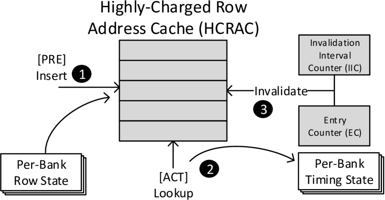
As we show in Figure 2, ChargeCache adds a small table (structured as a cache), called High-Charged Row Address Cache (HCRAC), to the memory controller that tracks the addresses of recently-accessed DRAM rows, i.e., highly-charged rows. ChargeCache performs three operations. First, when a precharge command is issued to a bank, ChargeCache inserts the address of the row that was activated in the corresponding bank to the table ( in the figure). Second, when an activate command is issued, ChargeCache checks if the corresponding row address is present in the table ( ). If the address is not present, then ChargeCache uses the standard DRAM timing parameters to issue subsequent commands to the bank. However, if the address of the activated row is present in the table, ChargeCache employs reduced timing parameters for subsequent commands to that bank. Our experimental results on multi-programmed applications show that, on average, ChargeCache can reduce the latency of 67% of all DRAM row activations (as shown in Section 6.4 of our HPCA 2016 paper [51]). Third, ChargeCache periodically invalidates old entries from the table to ensure that only rows that have sufficient amount of charge for being accessed with low latency remain in the table ( ). Since a row may potentially reside in the table for very long time without being activated, such an operation is necessary to avoid a low-latency access to a row with small amount of charge (which could lead to wrong results).
We name our mechanism ChargeCache, as it provides a cache-like benefit, i.e., latency reduction based on a locality property (i.e., RLTL), and does so by taking advantage of the charge level stored in a recently-activated row. The mechanism could potentially be used with current and emerging DRAM-based memories where the stored charge level leads to different access latencies. We release the source code of ChargeCache for two different versions of Ramulator [74, 122, 123] to enable future research to build upon our ideas.
6 Experimental Evaluation
In this section, we first explain our experimental methodology. Later, we quantitatively analyze the system performance improvement and DRAM energy savings that ChargeCache provides.
6.1 Methodology
We use circuit-level SPICE simulations to evaluate the DRAM latency reduction that can be achieved when accessing a highly-charged DRAM row. In Section 6.2, we show the reduction in two DRAM timing parameters, tRCD and tRAS, that are affected by high charge amount stored in a DRAM cell.222For detail on DRAM timing parameters and operation, we refer the reader to our prior works [73, 84, 83, 51, 127, 25, 27, 72, 71, 88, 82, 128, 87, 24, 52, 74, 114, 68].
To evaluate the performance of ChargeCache, we use a cycle-accurate DRAM simulator, Ramulator [74, 122], in CPU-trace-driven mode. CPU traces are collected using a Pintool [91]. Table 1 lists the configuration of the evaluated systems. We implement the HCRAC table, which ChargeCache uses to store the addresses of recently accessed DRAM rows, similarly to a 2-way associative cache that uses the LRU policy.
| Processor | 1-8 cores, 4GHz clock frequency, 3-wide issue, 8 MSHRs/core, 128-entry instruction window |
|---|---|
| Last-level Cache | 64B cache-line, 16-way associative, 4MB cache size |
| Memory Controller | 64-entry read/write request queues, FR-FCFS scheduling policy [121, 153], open/closed row policy [72, 71] for single/multi core |
| DRAM | DDR3-1600 [97], 800MHz bus frequency, 1/2 channels, 1 rank/channel, 8 banks/rank, 64K rows/bank, 8KB row-buffer size, tRCD/tRAS 11/28 cycles |
| ChargeCache | 128-entry (672 bytes)/core, 2-way associativity, LRU replacement policy, caching duration, tRCD/tRAS reduction 4/8 cycles |
For area, power, and energy measurements, we modify McPAT [85] to implement ChargeCache using process technology. We use DRAMPower [22] to obtain power/energy results for the off-chip main memory subsystem. We feed DRAMPower with DRAM command traces obtained from our simulations using Ramulator.
We run 22 workloads from the SPEC CPU2006 [137], TPC [147], and STREAM [94] benchmark suites. We use SimPoint [50] to obtain traces from representative phases of each application. For single-core evaluations, unless stated otherwise, we run each workload for 1 billion instructions. For multi-core evaluations, we use 20 multiprogrammed workloads by assigning a randomly-chosen application to each core. We evaluate each configuration with its best-performing row-buffer management policy. Specifically, we use the open-row policy for single-core and closed-row policy for multi-core configurations. We simulate the benchmarks until each core executes at least 1 billion instructions. For both single- and multi-core configurations, we first warm up the caches and ChargeCache by fast-forwarding 200 million cycles.
6.2 Reduction in DRAM Timing Parameters
We evaluate the potential reduction in tRCD and tRAS for ChargeCache using circuit-level SPICE simulations. We implement the DRAM sense amplifier circuit using DDR3 model parameters [119] and PTM low-power transistor models [152, 3]. Figure 3 plots the variation in bitline voltage level during cell activation for different initial charge amounts of the cell.
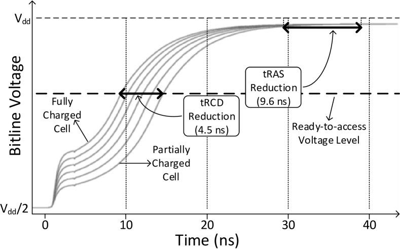
Depending on the initial charge (i.e., voltage level) of the cell, the bitline voltage increases at different speeds. When the cell is fully-charged, the sense amplifier is able to drive the bitline voltage to the ready-to-access voltage level in only . However, a partially-charged cell (i.e., one that has not been accessed for ) brings the bitline voltage up slower. Specifically, the bitline connected to such a partially-charged cell reaches the ready-to-access voltage level in . Since DRAM timing parameters are dictated by this worst-case partially-charged state right before the refresh interval, we can achieve a reduction in tRCD for a fully-charged cell. Similarly, the charge of the cell capacitor is restored at different times depending on the initial voltage of the cell. For a fully-charged cell, this results in a reduction in tRAS.
In practice, we expect DRAM manufacturers to identify the lowered timing constraints for different caching durations. Today, DRAM manufacturers test each DRAM chip to determine if it meets the timing specifications. Similarly, we expect the manufacturers would also test each chip to determine if it meets the ChargeCache timing constraints.
6.3 Results
We experimentally evaluate the following mechanisms: 1) ChargeCache, 2) NUAT [133], which accesses only rows that are recently-refreshed at lower latency than the DRAM standard, 3) ChargeCache + NUAT, which is a combination of ChargeCache and NUAT [133] mechanisms, and 4) Low-Latency DRAM (LL-DRAM) [96], which is an idealized comparison point where we assume all rows in DRAM can be accessed with low latency, compared to our baseline DDR3-1600 memory, at any time, irrespective of when they are accessed or refreshed.
We compare the performance of our mechanism against the most closely related previous work, NUAT [133]. The key idea of NUAT is to access recently-refreshed rows at low latency, because these rows are already highly-charged. Thus, NUAT does not use low latency for rows that are recently-accessed, and hence it does not exploit the RLTL (Row-Level Temporal Locality) present in many applications.
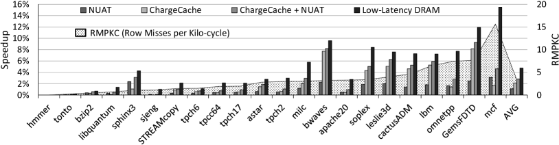
Figure 4 shows the performance of single-core and eight-core workloads. The figure also includes the number of row misses per kilo-cycles (RMPKC) to show row activation intensity, which provides insight into the RLTL of the workload.
Single-Core Performance: Figure 4(a) shows the performance improvement over the baseline system for single-core workloads. These workloads are sorted in ascending order of RMPKC. ChargeCache achieves up to 9.3% (an average of 2.1%) speedup. Our mechanism outperforms NUAT and achieves a speedup close to LL-DRAM with a few exceptions. Applications that have a wide gap in performance between ChargeCache and LL-DRAM (e.g., mcf, omnetpp) access a large number of DRAM rows and exhibit high row-reuse distance [63]. A high row-reuse distance indicates that there is a large number of accesses to other rows between two accesses to the same row. Due to this reason, ChargeCache cannot retain the addresses of highly-charged rows until the next access to that row. Increasing the number of ChargeCache entries or employing cache management policies aware of reuse distance or thrashing [35, 130, 117, 148] may improve the performance of ChargeCache for such applications. We leave the evaluation of these methods for future work. We conclude that ChargeCache significantly reduces execution time for most high-RMPKC workloads and outperforms NUAT for all but few workloads.
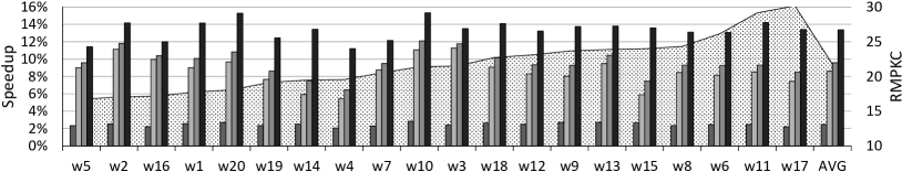
Eight-Core Performance: Figure 4(b) shows the speedup on eight-core multiprogrammed workloads. On average, ChargeCache and NUAT improve performance by 8.6% and 2.5%, respectively. Employing ChargeCache in combination with NUAT achieves a 9.6% speedup, which is only 3.8% less than the improvement obtained using LL-DRAM. Although the multiprogrammed workloads are composed of the same applications as in single-core evaluations, we observe much higher performance improvements for the eight-core workloads. The reason is twofold. First, since multiple cores share a limited capacity LLC, simultaneously running applications compete for the LLC. Thus, individual applications access main memory more often, which leads to higher RMPKC. This makes the workload performance more sensitive to main memory latency [20, 58, 73]. Second, the memory controllers receive memory requests from multiple simultaneously-running applications to a limited number of memory banks. Such requests are likely to target different rows since they use separate memory regions and these regions map to separate rows. Therefore, applications running concurrently exacerbate the bank-conflict rate and increase the number of row activations that hit in ChargeCache.
Overall, ChargeCache improves performance by up to 11.3% (8.1%) and on average 8.6% (2.1%) for eight-core (single-core) workloads. It outperforms NUAT for most of the applications. Using NUAT in combination with ChargeCache improves chsystem performance even further.
6.4 Impact on DRAM Energy
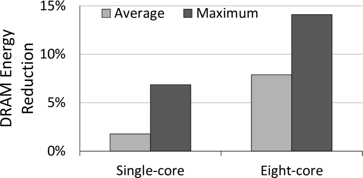
ChargeCache incurs negligible area and power overheads (see Section 6.5). Because it reduces execution time with negligible overhead, it leads to significant energy savings. Even though ChargeCache increases the energy efficiency of the entire system, we quantitatively evaluate the energy savings only for the DRAM subsystem since Ramulator [74] currently does not have a detailed CPU model. Figure 5 shows the average and maximum DRAM energy savings for single-core and eight-core workloads. ChargeCache reduces energy consumption by an average of 7.9% (1.8%), and by up to 14.1% (6.9%), for eight-core (single-core) workloads. We conclude that ChargeCache is effective at improving the energy efficiency of the DRAM subsystem, as well as the entire system.
6.5 Area and Power Consumption Overhead
HCRAC (Highly-Charged Row Address Cache) is the most area/power demanding component of ChargeCache. As we replicate HCRAC on a per-core and per-memory channel basis, the total area and power overhead ChargeCache introduces depends on the number of cores and memory channels.333Note that sharing a single HCRAC across all or multiple cores can result in even lower overhead. We leave the exploration of such shared-HCRAC designs to future work. The total storage requirement is given by Equation 1, where C are MC are the number of cores and memory channels, respectively. LRUbits depends on HCRAC associativity. EntrySize is calculated using Equation 2, where R, B, and Ro are the number of ranks, banks, and rows in DRAM, respectively.
|
|
(1) |
|
|
(2) |
Area. Our eight-core configuration has two memory channels. This introduces a total of 5376 bytes in storage requirement for a 128-entry HCRAC, corresponding to an area of . This overhead is only 0.24% of the 4MB LLC.
Power Consumption. HCRAC is accessed on every activate and precharge command issued by the memory controller. On an activate command, HCRAC is searched for the corresponding row address. On a precharge command, the address of the precharged row is inserted into HCRAC. HCRAC entries are periodically invalidated to ensure they do not exceed a specified caching duration. These three operations increase dynamic power consumption in the memory controller, and the HCRAC storage increases static power consumption. Our analysis indicates that ChargeCache consumes on average. This is only 0.23% of the average power consumption of the entire 4MB LLC. Note that we include the effect of this additional power consumption in our DRAM energy evaluations in Section 6.4. We conclude that ChargeCache incurs almost negligible chip area and power consumption overheads.
6.6 Other Results
We also evaluate and assess the sensitivity of ChargeCache benefits to ChargeCache capacity, caching duration, and temperature in Sections 6.4 and 7.1 of our HPCA 2016 paper [51].
7 Related Work
To our knowledge, this paper is the first to (i) show that applications typically exhibit significant Row-level Temporal Locality (RLTL) and (ii) exploit this locality to improve system performance by reducing the latency of requests to recently-accessed memory rows.
We have already (in Section 6.3) qualitatively and quantitatively compared ChargeCache to NUAT [133], which reduces access latency to only recently-refreshed rows. We have also shown that ChargeCache provides significantly higher average latency reduction than NUAT because RLTL is usually high, whereas the fraction of accesses to rows that are recently-refreshed is typically low (see Section 3 in our HPCA 2016 paper [51]).
Other previous works propose techniques to reduce performance degradation caused by long DRAM latencies. They focus on 1) enhancing the DRAM, 2) exploiting variations in manufacturing process and operating conditions, 3) developing various memory scheduling policies. We briefly summarize how ChargeCache differs from these works.
Enhancing DRAM Architecture. Lee at al. propose Tiered-Latency DRAM (TL-DRAM) [84], which divides each subarray into near and far segments using isolation transistors. With TL-DRAM, the memory controller accesses the near segment with lower latency since the isolation transistor reduces the bitline capacitance in that segment. Our mechanism could be implemented on top of TL-DRAM to reduce the access latency for both the near and far segment. Kim et al. propose SALP, which unlocks parallelism between subarrays at low cost, by modifying the DRAM chip to enable pipelined access to subarrays [73]. The goal of SALP is to reduce the impact of bank conflicts by providing more parallelism and thereby reducing the latency of bank-conflict accesses. O et al. [110] propose a DRAM architecture where sense amplifiers are decoupled from bitlines to mitigate precharge latency. Choi et al. [30] propose to utilize multiple DRAM cells to store a single bit when sufficient DRAM capacity is available. By using multiple cells, they reduce activation, precharge and refresh latencies. Other works [49, 136, 151, 127, 126, 128, 129, 26, 24, 79] also propose new DRAM architectures to lower DRAM latency for various types of operations and accesses.
Processing-in-memory (PIM) architectures [1, 2, 54, 53, 9, 128, 127, 129, 44, 41, 34, 65, 75, 111, 116, 132, 139, 69, 8] using 3D-stacked memory [81, 59, 56, 89] reduce the observed latency, from the perspective of the processor, by moving some computation operations closer to DRAM. 3D-stacked memories are well suited for processing-in-memory due to their inclusion of a logic layer, which allows for the efficient implementation of CMOS logic in DRAM and offers high bandwidth to the DRAM layers. However, PIM architectures do not fundamentally reduce the access latency of the DRAM device, which ChargeCache does (for certain access patterns).
Unlike ChargeCache, a large number of these works require changes to the DRAM architecture itself. The approaches taken by these works are largely orthogonal to the ChargeCache approach and ChargeCache could be implemented together with any of these mechanisms to further reduce the DRAM latency.
Exploiting Process and Operating Condition Variations. Recent studies [82, 25, 27, 83, 21] propose methods to reduce the safety margins of the DRAM timing parameters when operating conditions are appropriate (i.e., not worst-case). Unlike these works, ChargeCache is largely independent of operating conditions like temperature, as discussed in Section 8.3, and is orthogonal to these latency reduction mechanisms.
Memory Request Scheduling Policies. Memory request scheduling policies (e.g., [77, 121, 105, 106, 71, 72, 140, 142, 143, 149, 141, 4, 99, 153, 57, 100, 66, 45, 55]) reduce the average DRAM access latency by improving DRAM parallelism, row buffer locality, and fairness in especially multi-core and heterogeneous systems. ChargeCache can be employed in conjunction with the scheduling policy that best suits the application and the underlying architecture.
8 Significance
Main memory latency has a critical impact on system performance [101]. Our work proposes a new low-cost mechanism to reduce DRAM latency, without any modifications to the existing DRAM chip architecture. In this section, we discuss the significance of our work by describing its novelty and expected long-term impact.
8.1 Novelty
ChargeCache reduces average DRAM latency by exploiting a type of DRAM access locality, Row-Level Temporal Locality (RLTL), that commonly exists in workloads due to the presence of DRAM bank conflicts. Our work is the first to observe and formally define RLTL and exploit it to reduce DRAM latency by designing a new mechanism that takes advantage of RLTL and the fact that a DRAM row gets inherently refreshed on access. Our mechanism does not require any changes to the existing DRAM array structure of the DRAM chips and can be easily implemented on top of any DRAM standard with negligible overhead in the memory controller logic.
8.2 Applicability to Emerging DRAM Standards
ChargeCache is applicable to any memory technology where cells are volatile (leak charge over time) and the charge variation due to charge leakage has impact on access latency. ChargeCache can be used with to a large set of standards derived from DDR (DDRx, GDDRx, LPDDRx, etc.) [74] in a manner similar to the mechanism described in this work, without modifying the DRAM architecture. Using ChargeCache with 3D-stacked memories [81, 89] such as Wide I/O, HBM, and HMC [74] is also straightforward. The difference is that, for the technologies that implement the memory controller in the logic layer, the DRAM controller, and hence ChargeCache, can be easily implemented in the logic layer of the 3D-stacked memory chip instead of the processor chip.
8.3 Long-Term Impact
8.3.1 Reducing DRAM Latency
During the last several decades, DRAM capacity increased significantly by shrinking the feature size of the transistors. Similarly, more efficient DRAM standards enabled memories with high bandwidth. The new 3D-stacking technology offers even higher bandwidth by incorporating DRAM and the logic layer on the same chip in a 3D-stacked manner. However, none of these advances lead to large improvements in the row access latency of the DRAM arrays. Hence, DRAM latency is already a critical bottleneck for system performance. Our work alleviates the DRAM latency problem with no overhead to the area-optimized DRAM chip, which is difficult to change, and with low overhead to the memory controller.
8.3.2 Row-Level Temporal Locality
Our paper is the first work to observe row-level temporal locality (RLTL). Note that RLTL is different from Row-Reuse Distance [63] that a prior work studies. Row-Reuse Distance is a metric indicating the number of accesses between two consecutive accesses to the same row. On the other hand, RLTL indicates the time between two consecutive accesses to the same row. A row locality metric that includes time is important since charge leakage in DRAM is a function of time. In this work, we exploit RLTL to reduce DRAM latency. However, RLTL can also potentially be used to discover new techniques to improve different aspects of DRAM, such as reliability [70, 95, 101, 102] and bandwidth.
8.3.3 Importance for Future Systems
We believe the latency reduction mechanism of ChargeCache will become more important in future systems for four reasons. First, DRAM latency will become a much bigger bottleneck, as applications will become more data-intensive [101, 108]. Higher demand for data will result in more bank conflicts, as the number of DRAM banks is not scaling as fast as data intensity. Such applications will also have fast data access requirements, which will increase their sensitivity to the memory access latency [101, 108, 150, 43, 64]. As bank conflicts increase and accesses become more latency-critical, the benefits of ChargeCache will increase, as there will be higher RLTL, which ChargeCache can exploit to provide higher performance improvement.
Second, ChargeCache is likely to remain much more competitive than other state-of-the-art latency reduction techniques for the 3D-stacked memories of the future. These memories will likely operate at higher temperatures compared to conventional DRAM chips. The charge leakage rate of DRAM cells approximately doubles for every 10∘C increase in temperature [83, 87, 67, 114]. This observation can be exploited to lower the DRAM latency when operating at low temperatures. A previous study, Adaptive-Latency DRAM (AL-DRAM) [83], proposes a mechanism to improve system performance by reducing the DRAM timing parameters at low operating temperature. AL-DRAM is based on the premise that DRAM typically does not operate at temperatures close to the worst-case temperature (85∘ C) even when it is heavily accessed. However, new 3D-stacked DRAM technologies such as HMC, HBM, WideIO may operate at significantly higher temperatures due to tight integration of multiple stack layers [7]. Therefore, state-of-the-art and compelling dynamic latency scaling techniques such as AL-DRAM may be less useful in these scenarios. In contrast to AL-DRAM, ChargeCache is not based on the charge difference that occurs due to temperature dependence. Rather, we exploit the high level of charge in recently-precharged rows to reduce timing parameters during later accesses to such rows. After conducting tests to determine the possible latency reduction in accessing highly-charged rows (for ChargeCache hits) at worst-case temperatures, we show that ChargeCache can be employed independently of the operating temperature (see Section 7.1 in our HPCA 2016 paper [51]).
Third, ChargeCache is complementary to other temperature-based and structural DRAM latency reduction techniques [73, 84, 96, 136, 133, 82, 25, 24]. ChargeCache can easily be used in conjunction with any of these techniques.
Fourth, ChargeCache is a low-cost mechanism, which does not require any changes to the existing DRAM chips, and requires only small changes to the memory controller. The low cost makes the adoption of ChargeCache more feasible in future systems than other proposed mechanisms, as these systems will be bottlenecked by power consumption, and thus by complexity [108].
9 Conclusion
We introduce ChargeCache, a new, low-overhead mechanism that dynamically reduces the DRAM timing parameters for recently-accessed DRAM rows. ChargeCache exploits two key observations that we demonstrate in this work: 1) a recently-accessed DRAM row has cells with high amounts of charge and thus it can be accessed faster, and 2) many applications repeatedly access rows that are recently-accessed, due to bank conflicts.
Our extensive evaluations of ChargeCache on both single-core and multi-core systems show that it provides significant performance benefit and DRAM energy reduction at very modest hardware overhead. ChargeCache requires no modifications to the existing DRAM chips and occupies only a small area on the memory controller.
We conclude that ChargeCache is a simple yet efficient mechanism to dynamically reduce DRAM latency, which significantly improves both the performance and energy efficiency of modern systems. We hope that our observation of the phenomenon of row-level temporal locality and its simple exploitation to reduce DRAM latency inspires other works to develop other new techniques to improve memory subsystem characteristics like performance, efficiency, and reliability.
Acknowledgments
We thank Saugata Ghose for his dedicated effort in the preparation of this article. We thank the reviewers and the SAFARI group members for their feedback. We acknowledge the generous support of Google, Intel, NVIDIA, Samsung, and VMware. This work is supported in part by NSF grants 1212962, 1320531, and 1409723, the Intel Science and Technology Center for Cloud Computing, and the Semiconductor Research Corporation.
References
- [1] J. Ahn, S. Hong, S. Yoo, O. Mutlu, and K. Choi, “A Scalable Processing-in-Memory Accelerator for Parallel Graph Processing,” in ISCA, 2015.
- [2] J. Ahn, S. Yoo, O. Mutlu, and K. Choi, “PIM-Enabled Instructions: A Low-Overhead, Locality-Aware Processing-in-Memory Architecture,” in ISCA, 2015.
- [3] Arizona State Univ., NIMO Group, “Predictive Technology Model,” http://ptm.asu.edu/.
- [4] R. Ausavarungnirun, K. K.-W. Chang, L. Subramanian, G. H. Loh, and O. Mutlu, “Staged Memory Scheduling: Achieving High Performance and Scalability in Heterogeneous Systems,” in ISCA, 2012.
- [5] J.-L. Baer and T.-F. Chen, “An Effective on-Chip Preloading Scheme to Reduce Data Access Penalty,” in ICS, 1991.
- [6] M. Bekerman, S. Jourdan, R. Ronen, G. Kirshenboim, L. Rappoport, A. Yoaz, and U. Weiser, “Correlated Load-Address Predictors,” in ISCA, 1999.
- [7] B. Black et al., “Die Stacking (3D) Microarchitecture,” in MICRO, 2006.
- [8] A. Boroumand et al., “Google Workloads for Consumer Devices: Mitigating Data Movement Bottlenecks,” in ASPLOS, 2018.
- [9] A. Boroumand, S. Ghose, B. Lucia, K. Hsieh, K. Malladi, H. Zheng, and O. Mutlu, “LazyPIM: An Efficient Cache Coherence Mechanism for Processing-in-Memory,” IEEE CAL, 2017.
- [10] Y. Cai, S. Ghose, E. F. Haratsch, Y. Luo, and O. Mutlu, “Error Characterization, Mitigation, and Recovery in Flash Memory Based Solid-State Drives,” arXiv:1706.08642 [cs.AR], 2017.
- [11] Y. Cai, S. Ghose, E. F. Haratsch, Y. Luo, and O. Mutlu, “Errors in Flash-Memory-Based Solid-State Drives: Analysis, Mitigation, and Recovery,” arXiv:1711.11427 [cs.AR], 2017.
- [12] Y. Cai, S. Ghose, Y. Luo, K. Mai, O. Mutlu, and E. F. Haratsch, “Vulnerabilities in MLC NAND Flash Memory Programming: Experimental Analysis, Exploits, and Mitigation Techniques,” in HPCA, 2017.
- [13] Y. Cai, E. F. Haratsch, O. Mutlu, and K. Mai, “Error Patterns in MLC NAND Flash Memory: Measurement, Characterization, and Analysis,” in DATE, 2012.
- [14] Y. Cai, G. Yalcin, O. Mutlu, E. F. Haratsch, O. Unsal, A. Cristal, and K. Mai, “Neighbor Cell Assisted Error Correction in MLC NAND Flash Memories,” in SIGMETRICS, 2014.
- [15] Y. Cai, S. Ghose, E. F. Haratsch, Y. Luo, and O. Mutlu, “Error Characterization, Mitigation, and Recovery in Flash-Memory-Based Solid-State Drives,” Proc. IEEE, 2017.
- [16] Y. Cai, E. F. Haratsch, O. Mutlu, and K. Mai, “Threshold Voltage Distribution in MLC NAND Flash Memory: Characterization, Analysis, and Modeling,” in DATE, 2013.
- [17] Y. Cai, Y. Luo, S. Ghose, E. F. Haratsch, K. Mai, and O. Mutlu, “Read Disturb Errors in MLC NAND Flash Memory: Characterization, Mitigation, and Recovery,” in DSN, 2015.
- [18] Y. Cai, Y. Luo, E. F. Haratsch, K. Mai, and O. Mutlu, “Data Retention in MLC NAND Flash Memory: Characterization, Optimization, and Recovery,” in HPCA. IEEE, 2015.
- [19] Y. Cai, G. Yalcin, O. Mutlu, E. F. Haratsch, A. Cristal, O. S. Unsal, and K. Mai, “Flash Correct-and-Refresh: Retention-Aware Error Management for Increased Flash Memory Lifetime,” in ICCD, 2012.
- [20] D. Chandra, F. Guo, S. Kim, and Y. Solihin, “Predicting Inter-Thread Cache Contention on a Chip Multi-Processor Architecture,” in HPCA, 2005.
- [21] K. Chandrasekar, S. Goossens, C. Weis, M. Koedam, B. Akesson, N. Wehn, and K. Goossens, “Exploiting Expendable Process-Margins in DRAMs for Run-Time Performance Optimization,” in DATE, 2014.
- [22] K. Chandrasekar, C. Weis, B. Akesson, N. Wehn, and K. Goossens, “Towards Variation-Aware System-Level Power Estimation of DRAMs: An Empirical Approach,” in DAC, 2013.
- [23] K. K. Chang, “Understanding and Improving the Latency of DRAM-Based Memory Systems,” Ph.D. dissertation, Carnegie Mellon Univ., 2017.
- [24] K. K. Chang et al., “Low-Cost Inter-Linked Subarrays (LISA): Enabling Fast Inter-Subarray Data Movement in DRAM,” in HPCA, 2016.
- [25] K. K. Chang, A. Kashyap, H. Hassan, S. Ghose, K. Hsieh, D. Lee, T. Li, G. Pekhimenko, S. Khan, and O. Mutlu, “Understanding Latency Variation in Modern DRAM Chips: Experimental Characterization, Analysis, and Optimization,” in SIGMETRICS, 2016.
- [26] K. K. Chang, D. Lee, Z. Chishti, A. R. Alameldeen, C. Wilkerson, Y. Kim, and O. Mutlu, “Improving DRAM Performance by Parallelizing Refreshes with Accesses,” in HPCA, 2014.
- [27] K. K. Chang, A. G. Yaălikçi, S. Ghose, A. Agrawal, N. Chatterjee, A. Kashyap, D. Lee, M. O’Connor, H. Hassan, and O. Mutlu, “Understanding Reduced-Voltage Operation in Modern DRAM Devices: Experimental Characterization, Analysis, and Mechanisms,” SIGMETRICS, 2017.
- [28] M. J. Charney and T. R. Puzak, “Prefetching and Memory System Behavior of the SPEC95 Benchmark Suite,” IBM JRD, 1997.
- [29] N. Chatterjee, M. Shevgoor, R. Balasubramonian, A. Davis, Z. Fang, R. Illikkal, and R. Iyer, “Leveraging Heterogeneity in DRAM Main Memories to Accelerate Critical Word Access,” in MICRO, 2012.
- [30] J. Choi, W. Shin, J. Jang, J. Suh, Y. Kwon, Y. Moon, and L.-S. Kim, “Multiple Clone Row DRAM: A Low Latency and Area Optimized DRAM,” in ISCA, 2015.
- [31] Y. Chou, B. Fahs, and S. Abraham, “Microarchitecture Optimizations for Exploiting Memory-Level Parallelism,” in ISCA, 2004.
- [32] R. Das, R. Ausavarungnirun, O. Mutlu, A. Kumar, and M. Azimi, “Application-to-Core Mapping Policies to Reduce Memory System Interference in Multi-Core Systems,” in HPCA, 2013.
- [33] W. Ding, D. Guttman, and M. Kandemir, “Compiler Support for Optimizing Memory Bank-Level Parallelism,” in MICRO, 2014.
- [34] J. Draper et al., “The Architecture of the DIVA Processing-in-Memory Chip,” in ICS, 2002.
- [35] N. Duong, D. Zhao, T. Kim, R. Cammarota, M. Valero, and A. V. Veidenbaum, “Improving Cache Management Policies Using Dynamic Reuse Distances,” in MICRO, 2012.
- [36] E. Ebrahimi, C. J. Lee, O. Mutlu, and Y. N. Patt, “Prefetch-Aware Shared Resource Management for Multi-Core Systems,” in ISCA, 2011.
- [37] E. Ebrahimi, R. Miftakhutdinov, C. Fallin, C. J. Lee, J. A. Joao, O. Mutlu, and Y. N. Patt, “Parallel Application Memory Scheduling,” in MICRO, 2011.
- [38] E. Ebrahimi, O. Mutlu, C. J. Lee, and Y. N. Patt, “Coordinated Control of Multiple Prefetchers in Multi-Core Systems,” in MICRO, 2009.
- [39] E. Ebrahimi, O. Mutlu, and Y. N. Patt, “Techniques for Bandwidth-Efficient Prefetching of Linked Data Structures in Hybrid Prefetching Systems,” in HPCA, 2009.
- [40] R. J. Eickemeyer and S. Vassiliadis, “A Load-Instruction Unit for Pipelined Processors,” IBM JRD, 1993.
- [41] D. G. Elliott, M. Stumm, W. M. Snelgrove, C. Cojocaru, and R. McKenzie, “Computational RAM: Implementing Processors in Memory,” IEEE DT, 1999.
- [42] S. Eyerman and L. Eeckhout, “System-Level Performance Metrics for Multiprogram Workloads,” IEEE Micro, 2008.
- [43] M. Ferdman, A. Adileh, O. Kocberber, S. Volos, M. Alisafaee, D. Jevdjic, C. Kaynak, A. D. Popescu, A. Ailamaki, and B. Falsafi, “Clearing the Clouds: a Study of Emerging Scale-Out Workloads on Modern Hardware,” in ASPLOS, 2012.
- [44] B. B. Fraguela, J. Renau, P. Feautrier, D. Padua, and J. Torrellas, “Programming the FlexRAM Parallel Intelligent Memory System,” in PPoPP, 2003.
- [45] S. Ghose, H. Lee, and J. F. Martínez, “Improving Memory Scheduling via Processor-Side Load Criticality Information,” in ISCA, 2013.
- [46] M. Ghosh and H.-H. S. Lee, “Smart Refresh: An Enhanced Memory Controller Design for Reducing Energy in Conventional and 3D Die-Stacked DRAMs,” in MICRO, 2007.
- [47] A. Glew, “MLP yes! ILP no,” in ASPLOS WACI, 1998.
- [48] GSI, “Low Latency DRAMs,” http://www.gsitechnology.com.
- [49] N. D. Gulur, R. Manikantan, M. Mehendale, and R. Govindarajan, “Multiple Sub-Row Buffers in DRAM: Unlocking Performance and Energy Improvement Opportunities,” in ICS, 2012.
- [50] G. Hamerly, E. Perelman, J. Lau, and B. Calder, “Simpoint 3.0: Faster and More Flexible Program Phase Analysis,” JILP, 2005.
- [51] H. Hassan, G. Pekhimenko, N. Vijaykumar, V. Seshadri, D. Lee, O. Ergin, and O. Mutlu, “ChargeCache: Reducing DRAM Latency by Exploiting Row Access Locality,” in HPCA, 2016.
- [52] H. Hassan, N. Vijaykumar, S. Khan, S. Ghose, K. Chang, G. Pekhimenko, D. Lee, O. Ergin, and O. Mutlu, “SoftMC: A Flexible and Practical Open-Source Infrastructure for Enabling Experimental DRAM Studies,” in HPCA, 2017.
- [53] K. Hsieh, E. Ebrahimi, G. Kim, N. Chatterjee, M. O’Connor, N. Vijaykumar, O. Mutlu, and S. W. Keckler, “Transparent Offloading and Mapping (TOM): Enabling Programmer-Transparent Near-Data Processing in GPU Systems,” in ISCA, 2016.
- [54] K. Hsieh, S. Khan, N. Vijaykumar, K. K. Chang, A. Boroumand, S. Ghose, and O. Mutlu, “Accelerating Pointer Chasing in 3D-Stacked Memory: Challenges, Mechanisms, Evaluation,” in ICCD, 2016.
- [55] I. Hur and C. Lin, “Adaptive History-Based Memory Schedulers,” in MICRO, 2004.
- [56] Hybrid Memory Cube Consortium, “Hybrid Memory Cube specification 2.0,” November 2014.
- [57] E. Ipek, O. Mutlu, J. F. Martínez, and R. Caruana, “Self-Optimizing Memory Controllers: A Reinforcement Learning Approach,” in ISCA, 2008.
- [58] R. Iyer, L. Zhao, F. Guo, R. Illikkal, S. Makineni, D. Newell, Y. Solihin, L. Hsu, and S. Reinhardt, “QoS Policies and Architecture for Cache/Memory in CMP Platforms,” in SIGMETRICS, 2007.
- [59] JEDEC, “High Bandwidth Memory (HBM) DRAM,” 2013.
- [60] M. K. Jeong, D. H. Yoon, D. Sunwoo, M. Sullivan, I. Lee, and M. Erez, “Balancing DRAM Locality and Parallelism in Shared Memory CMP Systems,” in HPCA, 2012.
- [61] D. Jevdjic, G. H. Loh, C. Kaynak, and B. Falsafi, “Unison Cache: A Scalable and Effective Die-Stacked DRAM Cache,” in MICRO, 2014.
- [62] J. A. Joao, M. A. Suleman, O. Mutlu, and Y. N. Patt, “Bottleneck Identification and Scheduling in Multithreaded Applications,” in ASPLOS, 2012.
- [63] M. Kandemir, H. Zhao, X. Tang, and M. Karakoy, “Memory Row Reuse Distance and its Role in Optimizing Application Performance,” in SIGMETRICS, 2015.
- [64] S. Kanev, J. P. Darago, K. Hazelwood, P. Ranganathan, T. Moseley, G.-Y. Wei, and D. Brooks, “Profiling a Warehouse-Scale Computer,” in ISCA, 2015.
- [65] Y. Kang, W. Huang, S.-M. Yoo, D. Keen, Z. Ge, V. Lam, P. Pattnaik, and J. Torrellas, “FlexRAM: Toward an Advanced Intelligent Memory System,” in ICCD, 2012.
- [66] D. Kaseridis, J. Stuecheli, and L. K. John, “Minimalist Open-Page: A DRAM Page-Mode Scheduling Policy for the Many-Core Era,” in MICRO, 2011.
- [67] S. Khan, D. Lee, Y. Kim, A. R. Alameldeen, C. Wilkerson, and O. Mutlu, “The Efficacy of Error Mitigation Techniques for DRAM Retention Failures: A Comparative Experimental Study,” in SIGMETRICS, 2014.
- [68] J. S. Kim, M. Patel, H. Hassan, and O. Mutlu, “The DRAM Latency PUF: Quickly Evaluating Physical Unclonable Functions by Exploiting the Latency–Reliability Tradeoff in Modern DRAM Devices,” in HPCA, 2018.
- [69] J. S. Kim, D. Senol, H. Xin, D. Lee, S. Ghose, M. Alser, H. Hassan, O. Ergin, C. Alkan, and O. Mutlu, “GRIM-Filter: Fast Seed Location Filtering in DNA Read Mapping Using Processing-in-Memory Technologies,” BMC Genomics, 2018.
- [70] Y. Kim, R. Daly, J. Kim, C. Fallin, J. H. Lee, D. Lee, C. Wilkerson, K. Lai, and O. Mutlu, “Flipping Bits in Memory without Accessing Them: An Experimental Study of DRAM Disturbance Errors,” in ISCA, 2014.
- [71] Y. Kim, D. Han, O. Mutlu, and M. Harchol-Balter, “ATLAS: A Scalable and High-Performance Scheduling Algorithm for Multiple Memory Controllers,” in HPCA, 2010.
- [72] Y. Kim, M. Papamichael, O. Mutlu, and M. Harchol-Balter, “Thread Cluster Memory Scheduling: Exploiting Differences in Memory Access Behavior,” in MICRO, 2010.
- [73] Y. Kim, V. Seshadri, D. Lee, J. Liu, and O. Mutlu, “A Case for Exploiting Subarray-Level Parallelism (SALP) in DRAM,” in ISCA, 2012.
- [74] Y. Kim, W. Yang, and O. Mutlu, “Ramulator: A Fast and Extensible DRAM Simulator,” in CAL, 2015.
- [75] P. M. Kogge, “EXECUBE-a New Architecture for Scaleable MPPs,” in ICPP, 1994.
- [76] C. J. Lee, O. Mutlu, V. Narasiman, and Y. N. Patt, “Prefetch-Aware DRAM Controllers,” in MICRO, 2008.
- [77] C. J. Lee, V. Narasiman, E. Ebrahimi, O. Mutlu, and Y. N. Patt, “DRAM-aware Last-Level Cache Writeback: Reducing Write-Caused Interference in Memory Systems,” UT-Austin, HPS, Tech. Report, 2010.
- [78] C. J. Lee, V. Narasiman, O. Mutlu, and Y. N. Patt, “Improving Memory Bank-Level Parallelism in the Presence of refetching,” in MICRO, 2009.
- [79] D. Lee, L. Subramanian, R. Ausavarungnirun, J. Choi, and O. Mutlu, “Decoupled Direct Memory Access: Isolating CPU and IO Traffic by Leveraging a Dual-Data-Port DRAM,” in PACT, 2015.
- [80] D. Lee, “Reducing DRAM Latency at Low Cost by Exploiting Heterogeneity,” Ph.D. dissertation, Carnegie Mellon Univ., 2016.
- [81] D. Lee, S. Ghose, G. Pekhimenko, S. Khan, and O. Mutlu, “Simultaneous Multi-Layer Access: Improving 3D-Stacked Memory Bandwidth at Low Cost,” TACO, 2016.
- [82] D. Lee, S. Khan, L. Subramanian, S. Ghose, R. Ausavarungnirun, G. Pekhimenko, V. Seshadri, and O. Mutlu, “Design-Induced Latency Variation in Modern DRAM Chips: Characterization, Analysis, and Latency Reduction Mechanisms,” SIGMETRICS, 2017.
- [83] D. Lee, Y. Kim, G. Pekhimenko, S. Khan, V. Seshadri, K. Chang, and O. Mutlu, “Adaptive-Latency DRAM: Optimizing DRAM Timing for the Common-Case,” in HPCA, 2015.
- [84] D. Lee, Y. Kim, V. Seshadri, J. Liu, L. Subramanian, and O. Mutlu, “Tiered-Latency DRAM: A Low Latency and Low Cost DRAM Architecture,” in HPCA, 2013.
- [85] S. Li, J. H. Ahn, R. D. Strong, J. B. Brockman, D. M. Tullsen, and N. P. Jouppi, “McPAT: An Integrated Power, Area, and Timing Modeling Framework for Multicore and Manycore Architectures,” in MICRO, 2009.
- [86] E. Lindholm, J. Nickolls, S. Oberman, and J. Montrym, “NVIDIA Tesla: A Unified Graphics and Computing Architecture,” IEEE Micro, 2008.
- [87] J. Liu, B. Jaiyen, Y. Kim, C. Wilkerson, and O. Mutlu, “An Experimental Study of Data Retention Behavior in Modern DRAM Devices: Implications for Retention Time Profiling Mechanisms,” in ISCA, 2013.
- [88] J. Liu, B. Jaiyen, R. Veras, and O. Mutlu, “RAIDR: Retention-Aware Intelligent DRAM Refresh,” in ISCA, 2012.
- [89] G. H. Loh, “3D-Stacked Memory Architectures for Multi-Core Processors,” in ISCA, 2008.
- [90] P. Lotfi-Kamran et al., “Scale-Out Processors,” in ISCA, 2012.
- [91] C.-K. Luk, R. Cohn, R. Muth, H. Patil, A. Klauser, G. Lowney, S. Wallace, V. J. Reddi, and K. Hazelwood, “Pin: Building Customized Program Analysis Tools with Dynamic Instrumentation,” in PLDI, 2005.
- [92] Y. Luo, S. Ghose, Y. Cai, E. F. Haratsch, and O. Mutlu, “Enabling Accurate and Practical Online Flash Channel Modeling for Modern MLC NAND Flash Memory,” JSAC, 2016.
- [93] Y. Luo, S. Ghose, Y. Cai, E. F. Haratsch, and O. Mutlu, “HeatWatch: Improving 3D NAND Flash Memory Device Reliability by Exploiting Self-Recovery and Temperature Awareness,” in HPCA, 2018.
- [94] J. D. McCalpin, “STREAM Benchmark,” http://www.streambench.org/.
- [95] J. Meza, Q. Wu, S. Kumar, and O. Mutlu, “Revisiting Memory Errors in Large-Scale Production Data Centers: Analysis and Modeling of New Trends from the Field,” in DSN, 2015.
- [96] Micron, “RLDRAM Memory,” http://www.micron.com/products/dram/rldram-memory.
- [97] Micron Technology, “4Gb: x4, x8, x16 DDR3 SDRAM,” 2011.
- [98] T. Moscibroda and O. Mutlu, “Memory Performance Attacks: Denial of Memory Service in Multi-Core Systems,” in USENIX Security, 2007.
- [99] T. Moscibroda and O. Mutlu, “Distributed Order Scheduling and its Application to Multi-Core DRAM Controllers,” in PODC, 2008.
- [100] J. Mukundan and J. F. Martinez, “MORSE: Multi-Objective Reconfigurable Self-Optimizing Memory Scheduler,” in HPCA, 2012.
- [101] O. Mutlu, “Memory Scaling: A Systems Architecture Perspective,” in IMW, 2013.
- [102] O. Mutlu, “The RowHammer Problem and Other Issues We May Face as Memory Becomes Denser,” in DATE, 2017.
- [103] O. Mutlu, H. Kim, and Y. N. Patt, “Address-Value Delta (AVD) Prediction: Increasing the Effectiveness of Runahead Execution by Exploiting Regular Memory Allocation Patterns,” in MICRO, 2005.
- [104] O. Mutlu, H. Kim, and Y. N. Patt, “Techniques for Efficient Processing in Runahead Execution Engines,” in ISCA, 2005.
- [105] O. Mutlu and T. Moscibroda, “Stall-Time Fair Memory Access Scheduling for Chip Multiprocessors,” in MICRO, 2007.
- [106] O. Mutlu and T. Moscibroda, “Parallelism-Aware Batch Scheduling: Enhancing Both Performance and Fairness of Shared DRAM Systems,” in ISCA, 2008.
- [107] O. Mutlu, J. Stark, C. Wilkerson, and Y. N. Patt, “Runahead Execution: An Alternative to Very Large Instruction Windows for Out-of-Order Processors,” in HPCA, 2003.
- [108] O. Mutlu and L. Subramanian, “Research Problems and Opportunities in Memory Systems,” SUPERFRI, 2014.
- [109] P. Nair, C.-C. Chou, and M. K. Qureshi, “A Case for Refresh Pausing in DRAM Memory Systems,” in HPCA, 2013.
- [110] S. O, Y. H. Son, N. S. Kim, and J. H. Ahn, “Row-Buffer Decoupling: A Case for Low-Latency DRAM Microarchitecture,” in ISCA, 2014.
- [111] M. Oskin, F. T. Chong, and T. Sherwood, “Active Pages: A Computation Model for Intelligent Memory,” in ISCA, 1998.
- [112] V. S. Pai and S. Adve, “Code Transformations to Improve Memory Parallelism,” in MICRO, 1999.
- [113] S. Palacharla and R. Kessler, “Evaluating Stream Buffers as a Secondary Cache Replacement,” in ISCA, 1994.
- [114] M. Patel, J. S. Kim, and O. Mutlu, “The Reach Profiler (REAPER): Enabling the Mitigation of DRAM Retention Failures via Profiling at Aggressive Conditions,” in ISCA, 2017.
- [115] Y. N. Patt, W.-m. Hwu, and M. Shebanow, “HPS, A New Microarchitecture: Rationale and Introduction,” in MICRO, 1985.
- [116] D. Patterson, T. Anderson, N. Cardwell, R. Fromm, K. Keeton, C. Kozyrakis, R. Thomas, and K. Yelick, “A Case for Intelligent RAM,” IEEE Micro, 1997.
- [117] M. K. Qureshi, A. Jaleel, Y. N. Patt, S. C. Steely, and J. Emer, “Adaptive Insertion Policies for High Performance Caching,” in ISCA, 2007.
- [118] M. K. Qureshi, M. A. Suleman, and Y. N. Patt, “Line Distillation: Increasing Cache Capacity by Filtering Unused Words in Cache Lines,” in HPCA, 2007.
- [119] Rambus, “DRAM Power Model (2010),” http://www.rambus.com/energy.
- [120] B. R. Rau, “Pseudo-Randomly Interleaved Memory,” in ISCA, 1991.
- [121] S. Rixner, J. D. Owens, P. Mattson, U. J. Kapasi, and W. J. Dally, “Memory Access Scheduling,” in ISCA, 2000.
- [122] SAFARI Research Group, “Ramulator – GitHub Repository,” https://github.com/CMU-SAFARI/ramulator.
- [123] SAFARI Research Group, “RamulatorSharp – GitHub Repository,” https://github.com/CMU-SAFARI/RamulatorSharp.
- [124] SAFARI Research Group, “SAFARI Software Tools – GitHub Repository,” https://github.com/CMU-SAFARI.
- [125] Y. Sato et al., “Fast Cycle RAM (FCRAM); A 20-ns Random Row Access, Pipe-Lined Operating DRAM,” in VLSI Circuits, 1998.
- [126] V. Seshadri, K. Hsieh, A. Boroumand, D. Lee et al., “Fast Bulk Bitwise AND and OR in DRAM,” in CAL, 2015.
- [127] V. Seshadri et al., “RowClone: Fast and Energy-Efficient in-DRAM Bulk Data Copy and Initialization,” in MICRO, 2013.
- [128] V. Seshadri, D. Lee, T. Mullins, H. Hassan, A. Boroumand, J. Kim, M. A. Kozuch, O. Mutlu, P. B. Gibbons, and T. C. Mowry, “Ambit: In-Memory Accelerator for Bulk Bitwise Operations Using Commodity DRAM Technology,” in MICRO, 2017.
- [129] V. Seshadri, T. Mullins, A. Boroumand, O. Mutlu, P. B. Gibbons, M. A. Kozuch, and T. C. Mowry, “Gather-Scatter DRAM: In-DRAM Address Translation to Improve the Spatial Locality of Non-Unit Strided Accesses,” in MICRO, 2015.
- [130] V. Seshadri, O. Mutlu, M. A. Kozuch, and T. C. Mowry, “The Evicted-Address Filter: A Unified Mechanism to Address Both Cache Pollution and Thrashing,” in PACT, 2012.
- [131] V. Seshadri, S. Yedkar, H. Xin, O. Mutlu, P. B. Gibbons, M. A. Kozuch, and T. C. Mowry, “Mitigating Prefetcher-Caused Pollution Using Informed Caching Policies for Prefetched Blocks,” TACO, 2015.
- [132] D. E. Shaw, S. Stolfo, H. Ibrahim, B. K. Hillyer, J. Andrews, and G. Wiederhold, “The NON-VON Database Machine: An Overview,” Columbia Univ. Dept. of Computer Science, Tech. Rep. CUCS-022-81, 1981.
- [133] W. Shin, J. Yang, J. Choi, , and L.-S. Kim, “NUAT: A Non-Uniform Access Time Memory Controller,” in HPCA, 2014.
- [134] B. J. Smith, “A Pipelined, Shared Resource MIMD Computer,” in ICPP, 1978.
- [135] A. Snavely and D. M. Tullsen, “Symbiotic Jobscheduling for a Simultaneous Mutlithreading Processor,” ASPLOS, 2000.
- [136] Y. H. Son, O. Seongil, Y. Ro, J. W. Lee, and J. H. Ahn, “Reducing Memory Access Latency with Asymmetric DRAM Bank Organizations,” in ISCA, 2013.
- [137] SPEC CPU2006, “Standard Performance Evaluation Corporation,” http://www.spec.org/cpu2006.
- [138] S. Srinath, O. Mutlu, H. Kim, and Y. N. Patt, “Feedback Directed Prefetching: Improving the Performance and Bandwidth-Efficiency of Hardware Prefetchers,” in HPCA, 2007.
- [139] H. S. Stone, “A Logic-in-Memory Computer,” IEEE Trans. Comput., 1970.
- [140] L. Subramanian, D. Lee, V. Seshadri, H. Rastogi, and O. Mutlu, “The Blacklisting Memory Scheduler: Achieving High Performance and Fairness at Low Cost,” in ICCD, 2014.
- [141] L. Subramanian, D. Lee, V. Seshadri, H. Rastogi, and O. Mutlu, “The Blacklisting Memory Scheduler: Balancing Performance, Fairness and Complexity,” TPDS, 2015.
- [142] L. Subramanian, V. Seshadri, A. Ghosh, S. Khan, and O. Mutlu, “The Application Slowdown Model: Quantifying and Controlling the Impact of Inter-Application Interference at Shared Caches and Main Memory,” in MICRO, 2015.
- [143] L. Subramanian, V. Seshadri, Y. Kim, B. Jaiyen, and O. Mutlu, “MISE: Providing Performance Predictability and Improving Fairness in Shared Main Memory Systems,” in HPCA, 2013.
- [144] M. A. Suleman, O. Mutlu, M. K. Qureshi, and Y. N. Patt, “Accelerating Critical Section Execution with Asymmetric Multi-Core Architectures,” in ASPLOS, 2009.
- [145] J. E. Thornton, “Parallel Operation in the Control Data 6600,” in Fall Joint Computer Conference, 1964.
- [146] R. M. Tomasulo, “An Efficient Algorithm for Exploiting Multiple Arithmetic Units,” IBM JRD, 1967.
- [147] Transaction Processing Performance Council, “TPC Benchmarks,” http://www.tpc.org/.
- [148] G. Tyson, M. Farrens, J. Matthews, and A. R. Pleszkun, “A Modified Approach to Data Cache Management,” in MICRO, 1995.
- [149] H. Usui, L. Subramanian, K. K.-W. Chang, and O. Mutlu, “DASH: Deadline-Aware High-Performance Memory Scheduler for Heterogeneous Systems with Hardware Accelerators,” TACO, 2016.
- [150] L. Wang et al., “BigDataBench: A Big Data Benchmark Suite from Internet Services,” in HPCA, 2014.
- [151] T. Zhang, K. Chen, C. Xu, G. Sun, T. Wang, and Y. Xie, “Half-DRAM: A High-Bandwidth and Low-Power DRAM Architecture from the Rethinking of Fine-Grained Activation,” in ISCA, 2014.
- [152] W. Zhao and Y. Cao, “New Generation of Predictive Technology Model for Sub-45 nm Early Design Exploration,” IEEE TED, 2006.
- [153] W. K. Zuravleff and T. Robinson, “Controller for a Synchronous DRAM that Maximizes Throughput by Allowing Memory Requests and Commands to be Issued Out of Order,” US Patent 5,630,096. 1997.