Electro-optic polarization tuning of microcavities with a single quantum dot
Abstract
We present an oxide aperture microcavity with embedded quantum dots that utilizes a three contact design to independently tune the quantum dot wavelength and birefringence of the cavity modes. A polarization splitting tuning of 5 GHz is observed. For typical microcavity polarization splittings, the method can be used to achieve perfect polarization degeneracy that is required for many polarization-based implementations of photonic quantum gates. The embedded quantum dot wavelength can be tuned into resonance with the cavity, independent of the polarization tuning.
Semiconductor quantum dots (QDs) are promising candidates for various aspects of quantum information, such as single photon sources Somaschi2016 , remote-spin entanglement generation Delteil2016 ; Stockill2017 ; Wei2014 , generation of photonic cluster states Lindner2009 , and direct production of entangled photon pairs Benson2000 ; Stevenson2006 ; Muller2014 ; Trotta2014 . Scalable architectures, however, require a high collection efficiency of the emitted photons. For this reason it is necessary to embed the QDs in an optical microcavity to enhance emission into a single desired mode Senellart2017 . With the advances of cavity designs, high quality microcavities with embedded QDs can be routinely fabricated. Purcell enhancement Gerard1998 and strong coupling Reithmaier2004 of a single QD in a micropillar cavity have been demonstrated, and quality factors exceeding 250,000 have been reported Schneider2016 . The inevitable birefringence of such structures, however, presents an additional complication with ever increasing quality factors. For the implementation of polarization based quantum gates, it is necessary for an embedded QD to couple equally to both photon polarizations, and therefore to both orthogonally polarized cavity modes. Single photon sources often require resonant pulsed excitation, where it is impossible to eliminate all incident laser light with cross polarization if the cavity is birefringent over the spectral width of the laser.
Inherent material birefringence does not exist for the zinc-blende crystal structure. Polarization splitting of cavity modes arises primarily from electro-optic (EO) or elasto-optic birefringnece, and form birefringence from asymmetries of the fabricated cavity. QDs are typically embedded in a diode in order to tune their emission wavelength through the quantum confined Stark effect. Because of the linear EO effect, or Pockels effect, the applied field introduces birefringence. The built-in electric fields and strain in a heterostructure, either inherent from growth or the result of fabrication, also contribute to the polarization splitting of the cavity modes VanExter1997 ; Hendriks1997 . EO birefringence is the likely reason micropillar cavities often exhibit linearly polarized modes aligned with the major and minor axes of the crystal. Asymmetrical cavity shapes further contribute to polarization splitting, see Bava2001 ; Debernardi2002 for example. There has been a lot of work in fabricating microcavities with close to zero polarization splitting Bakker2015 ; Bonato2009 ; Bakker2014 , but a continuous fine tuning method is still needed.
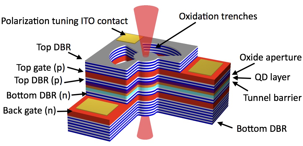
The device presented, shown in Figure 1, is a micropillar cavity with three contacts. The QDs are embedded in a p-i-n diode and surrounded by two distributed Bragg reflectors (DBRs). A transparent indium tin oxide (ITO) Schottky contact is deposited on the top of the device. Applying an electric field over the top mirror tunes the cavity polarization splitting through the Pockels effect. The electric field in the active region can be set independently to tune the QD into resonance with the cavity mode. Such a device has similarly been used to control the output polarization state of a vertical-cavity surface-emitting laser through modification of the optical gain of the polarized modes Park2000 . With polarization resolved reflection spectroscopy, we study the EO tuning on the scale of GHz and demonstrate complete restoration of the cavity polarization splitting. Electrical control of the embedded QD wavelength is retained while the cavity polarization splitting is tuned.
The Pockels effect is a second order effect in crystals that lack an inversion center Abeles1972 . For crystals in the 3m point group, including zinc-blende crystals, the linear electro-optic tensor has only 1 non-zero element, , assumed here to be real Adachi1984 . For an electric field applied along the axis, the crystal is bireferingent, and the corresponding principle axes of the crystal are defined by the major and minor axes. The induced birefringence from an applied DC field, , is described by
| (1) |
where is the real index with no field and refers to the real index of the and axes.
DBR mirrors have a large penetration depth, which allows a cavity resonance to be tuned by applying an electric field only over a single mirror. It is well known that an incident optical pulse undergoes a time delay and spreading in space upon reflection off of a dispersive mirror Babic1992 ; Laporta1985 . The time delay is important for characterizing the wavelength of a cavity, which to first order is defined by a linear phase slope, . The effective penetration depth of a hard mirror, , is given by
| (2) |
Equation 2 is evaluated at the Bragg condition, denoted . is used to model a dispersive mirror with a fixed phase mirror placed some distance from the actual mirror interface. In general, it is irrelevant what material is chosen to replace the resulting empty space, so long as the optical length is kept the same. For calculations involving cavities, it is most convenient to choose the material in front of the mirror to be the same material composing the spacer region of the cavity, denoted by . Analytical solutions for the penetration depth exist in the case of a single DBR mirror. For details the reader is referred to the literature Babic1992 ; Laporta1985 ; Coldren ; Corzine1991 .
The optical path length of the layers in a DBR are altered from the Pockels effect when a field is present; the Bragg frequency shifts as a result of an applied voltage. In the effective mirror model, the shift is equivalent to moving the mirror some distance, ,
| (3) |
is the frequency shift of the Bragg condition and is the group index of the spacer material. Considering a Fabry-Perot cavity formed from two identical DBR mirrors, described in the effective mirror model, with penetration depths given by Equation 2, and a spacer layer of length, , the cavity resonance shift can be calculated. The frequency shift of the cavity, , is given by
| (4) |
Equation 4 assumes that the second mirror is unaltered by the application of an electric field on the other, which is only true if the second mirror is non-dispersive. For two DBR mirrors, the cavity shift from the change in penetration depth of one mirror is accompanied by a change in penetration depth of the second. The coupling of both mirrors with a shift in cavity frequency must be taken into account. The parameter is introduced for simplicity. The total change in cavity resonance with coupled mirrors is given by adding the contributions of both mirrors,
| (5) |
is found from computing the new optical path length of a single period in the DBR with an applied field. The cavity polarization splitting is denoted . For small changes in the index of refraction of both materials composing the DBR cavity, and , the polarization splitting can be expressed as
| (6) |
The values and are the changes in refractive index for materials 1 and 2.
Equation 6 assumes two identical mirrors with a cavity resonance matching exactly the Bragg condition. Our devices have more complex designs than this simplified model. Nevertheless, the model can give a rough estimate of the expected tuning range with an applied voltage over a single mirror, and yield insight into the effects of various parameters that may be exploited to increase the tuning range.
Samples are grown with molecular beam epitaxy on an undoped GaAs substrate. Two DBR mirrors, composed of quarter wave layers (24 bottom layers and 22 top layers) of GaAs and AlGaAs, surrounding the active region form a Fabry-Perot cavity. InGaAs QDs are grown via Stranski-Krastanov growth in the active region. A large part of the DBR layers is undoped, and a 60 nm layer of ITO is deposited on top of the device to form a transparent Schottky contact. Microcavities with transverse confinement are fabricated by etching trenches with Cl2/BCl3/N2 inductively coupled plasma. Etching both exposes a high Al concentration layer, and provides access to the n and p doped contact layers. The sample is held in a tube furnace at C in steam for 1 hour for the oxidation process. The Al concentration is tapered along the oxide layer in order to create an intracavity lens Coldren1998 . Ni/AuGe/Ag/Au and Ti/Pt/Au contact pads are deposited on the n and p doped contact layers respectively to form Ohmic contacts. The ITO layer is contacted via a Cr/Ni/Au pad, and all three pads are wire bonded to a custom submount before mounting in a closed cycle cryostat operating at 6K.
Asymmetric apertures are likely the primary cause of initial birefringence in oxide aperture microcavities. In order to completely restore polarization degeneracy, the shape of the aperture must be controlled. The mesa in this study is made elliptical such that it is longer along the major axis to account for the difference in oxidation rates along the major and minor axes Choquette1996 ; Bakker2014 . By altering the aperture symmetry, the polarization can be coarsely tuned to degeneracy and EO tuning is used as a fine control.
Reflection spectroscopy on the lowest order HE11 Gaussian modes of the cavity reveals in detail the behavior of the modes with EO tuning. Figure 2 shows the typical tuning behavior of the modes, denoted H and V, as a bias is applied to the top contact. The p-i-n region is held at a fixed voltage with respect to the p contact. H corresponds to the major axis of the crystal, . The modes cross around -5 V implying the existence of a configuration that gives a completely polarization degenerate cavity. In addition, there is an absolute shift of the cavity resonance, which can be explained by quadratic EO effects that do not exhibit birefringence: Kerr effect, etc.
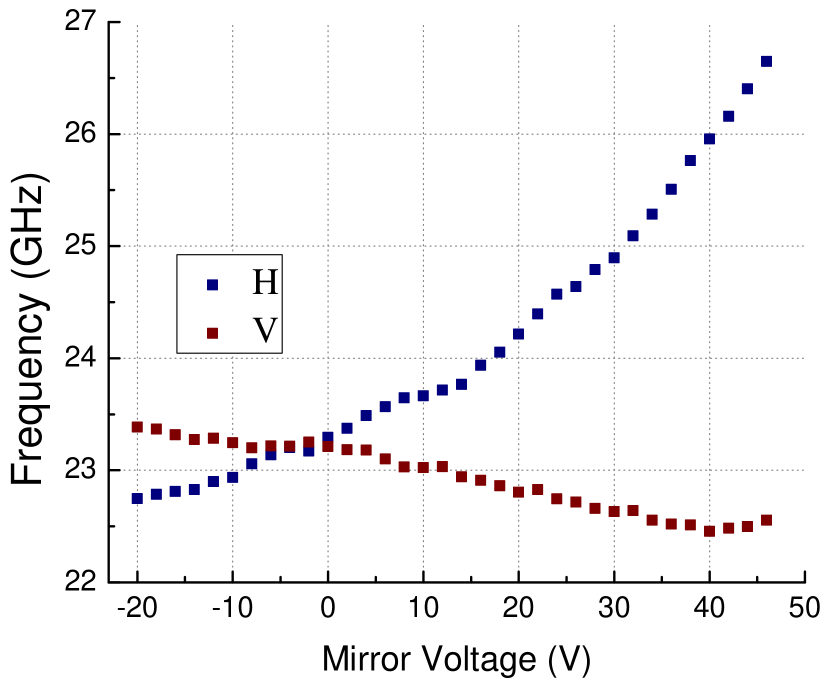
The tuning range observed experimentally is aproximately 4.5 GHz, which is non-destructive and reversible. Parameters derived from the device design yield a penetration depth, nm, and the spacer layer thickness is, nm. Values for the linear EO coefficient are taken to be and for GaAs and AlGaAs respectively Berseth1992 . An estimate of the tuning range using equation 6 then yields GHz. The theoretical model is verified with transmission matrix method (TMM) calulations. TMM on a simplified symmetric cavity yields a tuning range of 2.2 GHz. The TMM calculation for the full device structure yields a tuning range of 0.73 GHz, about 5 times less than observed in the experiment.
Several effects could explain the deviation of the observed shift from theory. In addition to the deviation from theory we observe a increase in the width of the H mode at high fields but not for the V mode. The device layout has contacts oriented along the major axis and small transverse currents could introduce free carrier losses for only the H mode. Although mirror absorption can alter the phase dispersion, the observed increase in width does not correspond to values of absorption that are expected to result in measurable shifts of the cavity resonance. For transverse fields applied to the device, quadratic EO effects can induce birefringence. Typical values of the quadratic EO coefficient for GaAs are small, but very dispersive around the band gap Berseth1992 . Large quadratic effects have additionally been observed in complicated waveguide heterostructures Glick1986 ; Wood1987 .
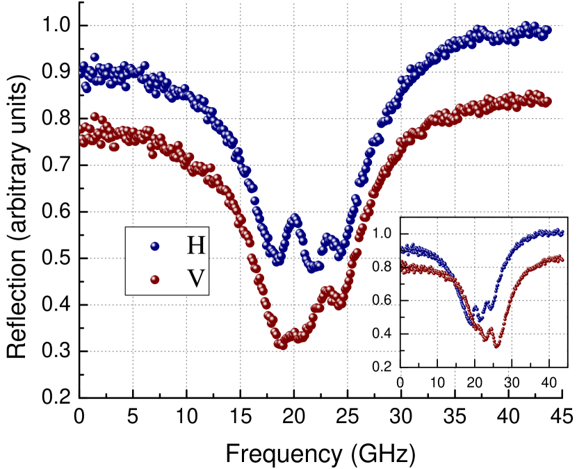
The QD-microcavity system must be excited in the cavity polarization basis when the polarization degeneracy is large. An example of this, albeit with small polarization splitting, is shown in Figure 3. H and V denote the cavity basis. In the reflection spectrum of the cavity, the QD appears as a peak in the cavity mode, which is due to the excitation of an electron-hole pair of a neutral dot. The fine structure splitting of the QD is clearly visible as two peaks. The inset shows the same measurement for the case of imperfect polarization degeneracy.
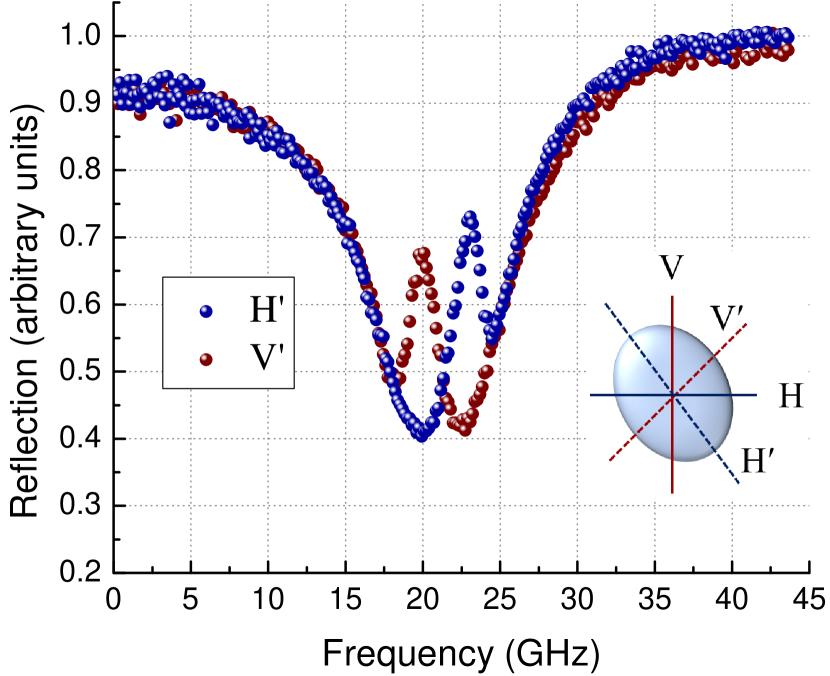
Self-assembled InGaAs QDs grown on substrates are typically not oriented along either the major or minor crystal axis. The resulting cavity-QD system, therefore, has a cavity polarization basis and QD polarization basis. Maximum coupling of photons to exciton transitions can be accomplished in the case of identical cavity and QD basis, or when the cavity is polarization degenerate. The latter is shown in Figure 4, which shows the reflection spectrum in the QD basis, denoted as H′ and V′, approximately 45∘ from the cavity basis. For either exciton transition, the coupling to the cavity mode is stronger than in the cavity basis, evident by the higher peaks in reflectivity.
State of the art single photon sources require pulsed excitation Senellart2017 for which the light uncoupled to a QD must be extinguished. Cavity polarization splitting, however, results in spectrally dependent rotations of uncoupled incident laser light, which limits the purity of a single photon source. The presence of a cavity basis and exciton basis further restricts the possible polarization angles for efficient single photon emission into a cavity mode Anton2017 . These issues can be remedied only with a polarization degenerate cavity.
We have demonstrated that a three contact microcavity design gives an extra knob to control the polarization splitting of microcavities, and allows simultaneous electrical control of the embedded QDs. The method can be extended to more conventional air guided micropillar cavities Somaschi2016 , and/or combined with aditional tuning techniques, such as strain, which can address the fine structure splitting of the dots. The fabrication process is compatible with methods of identifying particular dots prior to fabrication that deterministically control the QD properties and coupling to the cavity Dousse2008 . The QD studied here is a neutral dot. For charged QDs, which exhibit circularly polarized transitions, polarization degeneracy of the cavity is even more important. Several proposals are available for trapping single electrons or spins Heiss2009 ; Mar2014 , and electron spins have been demonstrated in photonic crystal cavities Carter2013 . Together with polarization degenerate cavities, this system would have all the necessary ingredients for efficient photonic quantum gates and spin-photon entanglement schemes.
Funding. Foundation for Fundamental Research on Matter-Netherlands Organisation for Scientific Research (FOM-NWO) (08QIP6-2) as part of the Frontiers of Nanoscience program; National Science Foundation (NSF) (0901886, 0960331).
Acknowledgments. The authors would like to acknowledge A. Kerr for sample characterization, and B. J. Thibeault and D. D. John for fruitful discussions.
References
- (1) N. Somaschi et al., Nature Photonics 10, 340 (2016).
- (2) A. Delteil et al., Nature Physics 12, 218 (2016).
- (3) R. Stockill et al., Physical Review Letters 119, 010503 (2017).
- (4) H.-R. Wei and F.-G. Deng, Optics Express 22, 593 (2014).
- (5) N. H. Lindner and T. Rudolph, Physical Review Letters 103, 113602 (2009).
- (6) O. Benson, C. Santori, M. Pelton, and Y. Yamamoto, Physical Review Letters 84, 2513 (2000).
- (7) R. M. Stevenson et al., Nature 439, 179 (2006).
- (8) M. Müller, S. Bounouar, K. D. Jöns, M. Glässl, and P. Michler, Nature Photonics 8, 224 (2014).
- (9) R. Trotta, J. S. Wildmann, E. Zallo, O. G. Schmidt, and A. Rastelli, Nano Letters 14, 3439 (2014).
- (10) P. Senellart, G. Solomon, and A. White, Nature Nanotechnology 12, 1026 (2017).
- (11) J. Gérard et al., Physical Review Letters 81, 1110 (1998).
- (12) J. P. Reithmaier et al., Nature 432, 197 (2004).
- (13) C. Schneider, P. Gold, S. Reitzenstein, S. Höfling, and M. Kamp, Applied Physics B 122, 19 (2016).
- (14) M. P. van Exter, A. K. Jansen van Doorn, and J. P. Woerdman, Physical Review A 56, 845 (1997).
- (15) R. F. M. Hendriks et al., Applied Physics Letters 71, 2599 (1997).
- (16) G. P. Bava, P. Debernardi, and L. Fratta, Physical Review A 63, 023816 (2001).
- (17) P. Debernardi, G. Bava, C. Degen, I. Fischer, and W. Elsasser, IEEE Journal of Quantum Electronics 38, 73 (2002).
- (18) M. P. Bakker et al., Physical Review B 91, 115319 (2015).
- (19) C. Bonato et al., Applied Physics Letters 95, 251104 (2009).
- (20) M. P. Bakker et al., Applied Physics Letters 104, 151109 (2014).
- (21) M. S. Park et al., Applied Physics Letters 76, 813 (2000).
- (22) F. Abeles, Optical Properties of Solids (, 1972).
- (23) S. Adachi and K. Oe, Journal of Applied Physics 56 (1984).
- (24) D. Babic and S. Corzine, IEEE Journal of Quantum Electronics 28, 514 (1992).
- (25) P. Laporta and V. Magni, Applied Optics 24, 2014 (1985).
- (26) L. A. Coldren, S. W. Corzine, and M. L. Milan, Diode Lasers and Photonic Integrated Circuits, Second ed. .
- (27) S. Corzine, R. Yan, and L. Coldren, IEEE Journal of Quantum Electronics 27, 2086 (1991).
- (28) L. A. Coldren, B. J. Thibeault, E. R. Hegblom, G. B. Thompson, and J. W. Scott, Applied Physics Letters 68, 313 (1996).
- (29) K. D. Choquette et al., Applied Physics Letters 69, 1385 (1996).
- (30) C.-A. Berseth, C. Wuethrich, and F. K. Reinhart, Journal of Applied Physics 71 (1992).
- (31) M. Glick, F. K. Reinhart, G. Weimann, and W. Schlapp, Applied Physics Letters 48, 989 (1986).
- (32) T. H. Wood, R. W. Tkach, and A. R. Chraplyvy, Applied Physics Letters 50, 798 (1987).
- (33) C. Antón et al., Optica 4, 1326 (2017).
- (34) A. Dousse et al., Physical Review Letters 101, 267404 (2008).
- (35) D. Heiss et al., Applied Physics Letters 94, 072108 (2009).
- (36) J. D. Mar, J. J. Baumberg, X. Xu, A. C. Irvine, and D. A. Williams, Physical Review B 90 (2014).
- (37) S. G. Carter et al., Nature Photonics 7, 329 (2013).