Waveguide-Integrated Mid-Infrared Plasmonics with High-Efficiency Coupling for Ultracompact Surface-Enhanced Infrared Absorption Spectroscopy
Abstract
Waveguide-integrated plasmonics is a growing field with many innovative concepts and demonstrated devices in the visible and near-infrared. Here, we extend this body of work to the mid-infrared for the application of surface-enhanced infrared absorption (SEIRA), a spectroscopic method to probe molecular vibrations in small volumes and thin films. Built atop a silicon-on-insulator (SOI) waveguide platform, two key plasmonic structures useful for SEIRA are examined using computational modeling: gold nanorods and coaxial nanoapertures. We find resonance dips of 80% in near diffraction-limited areas due to arrays of our structures and up to 40% from a single resonator. Each of the structures are evaluated using the simulated SEIRA signal from poly(methyl methacrylate) and an octadecanethiol self-assembled monolayer. The platforms we present allow for a compact, on-chip SEIRA sensing system with highly efficient waveguide coupling in the mid-IR.
I Introduction
Much work has previously been performed on integrating plasmonicsref1 ; ref2 with low-loss dielectric photonic integrated circuits (PICs) in an effort to miniaturize free-space optical components into a compact, chip-based system orders of magnitude smaller and at lower cost. Broad potential applications have already been explored, such as surface-enhanced Raman spectroscopy (SERS)ref3 , hybrid lasersref4 , optical switchingref5 , directional waveguide couplingref6 , plasmon-enhanced optical forces in waveguidesref7 ; ref8 , two-plasmon quantum interferenceref9 , nanofocusingref10 ; ref11 , integration with two-dimensional (2D) materialsref12 ; ref13 ; ref14 , and refractive index sensingref15 . While most of this work is in the visible and near-infrared (NIR), the mid-infrared (MIR) has yet to be greatly explored. The MIR (typically 2-10 m in wavelengths) is an important regime for biochemical spectroscopies thanks to the vast number of chemical resonances present that can give detailed information regarding molecular structureref16 ; ref17 ; ref18 ; ref19 . The vibrational spectra of molecules are often measured with Fourier-Transform Infra-Red (FTIR) spectroscopy using broadband sources and free-space optics. However, with the advent of bright coherent MIR laser sources, MIR plasmonic antennasref20 , the maturation of silicon photonics technology, and the growing interest in ultrasensitive chemical identification and diagnostics, there is tremendous potential for waveguide-integrated MIR systems.
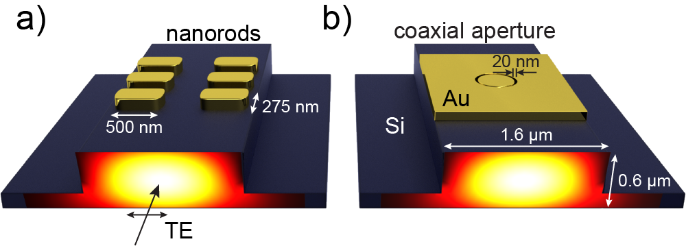
In this letter, we theoretically examine silicon waveguide-integrated plasmonics for surface-enhanced infrared absorption (SEIRA)ref21 ; ref22 ; ref23 ; ref24 ; ref25 ; ref26 ; ref27 ; ref28 spectroscopy using two common plasmonic resonator building blocks: nanorods and coaxial apertures (Figure 1). These structures have been studied in a free-space context for SEIRA, and have shown large performance improvements over standard infrared absorption techniques thanks to the field enhancement afforded by plasmonics, highly advantageous for thin films. Here, these same building blocks are arranged on a Si waveguide to perform obtain high coupling with a minimized footprint. The Si waveguide presented is designed based on a 600 nm silicon-on-insulator (SOI) wafer platform built for operation around 3 m, a common location for resonances based on C-H bond stretching. To maintain single-mode operation, the width of the waveguide is limited to 1.6 m, and a 200 nm thick support is used for releasing the waveguide from the oxide below. A schematic of the waveguide designed and the resonators proposed is available in Figure 1.
II Theory
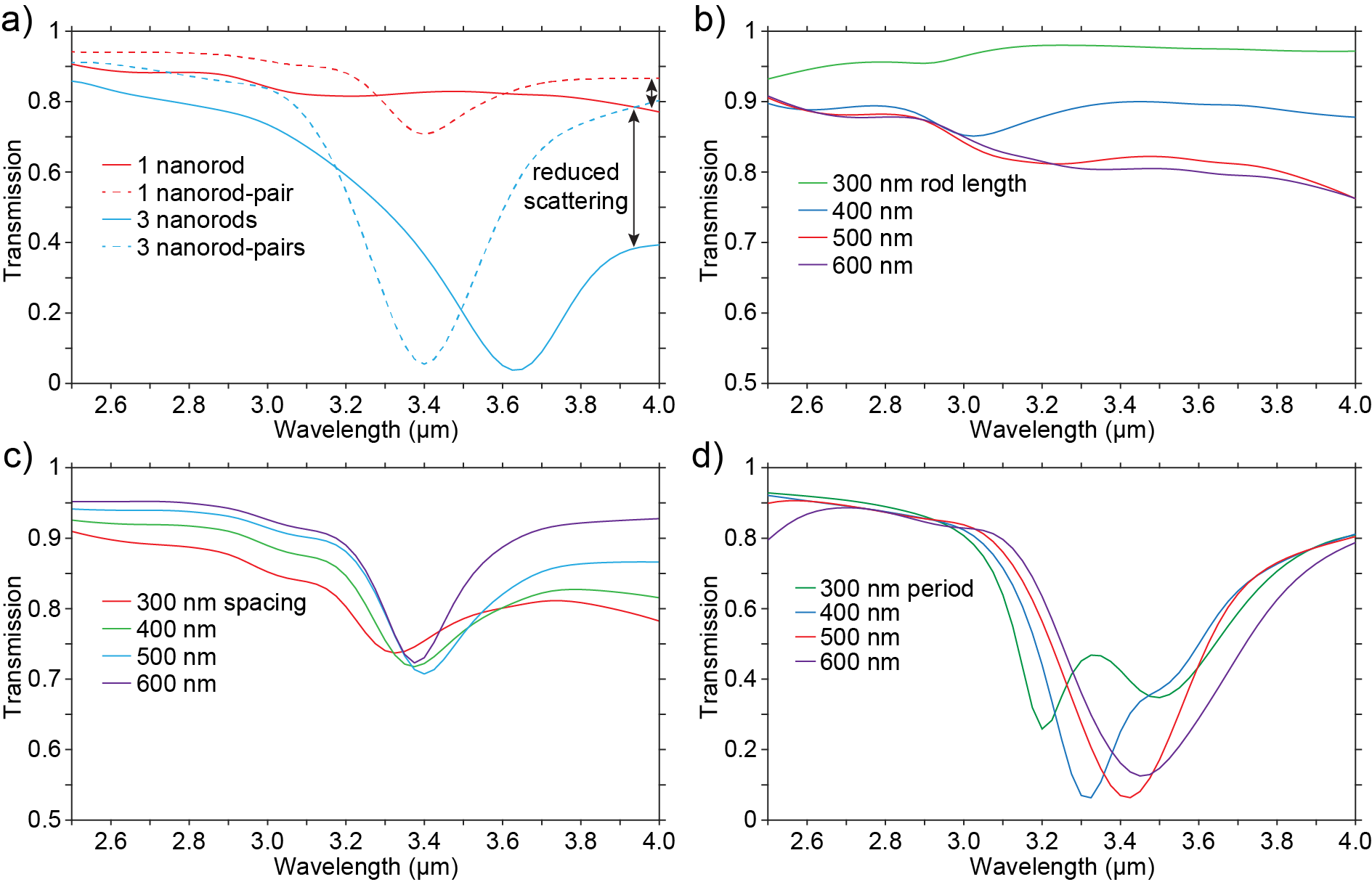
Metallic nanorods are a versatile building block for both waveguide-integrated plasmonics and resonant SEIRA. They are compact and can yield high field enhancements despite having such a simple geometry. While structures with few nanorods atop waveguides have already been fabricated and well-studied, we take this structure and tune it for use on MIR waveguides using dimensions similar to previous work in this arearef22 ; ref29 . Using these parameters combined with our waveguide design, we find that pairs of nanorods placed on the waveguide yield efficient structures with lower scattering outside of the resonant wavelength compared to arrays of single rods (Figures 2a and 6a). To further increase the resonance dip in waveguide transmission, multiple pairs are placed in close proximity to allow coupling (Figure 2a). We find that this design shows similar field enhancement to the far-field array version of this device (Figures 2b,c, and 7), while drastically reducing the excitation area from the spot-size of a typical FTIR light source (100) to a diffraction-limited area ( when measured outside the waveguide). This allows for both the miniaturization to a chip-based device while also pushing the limit of detection closer to single-particle levels. In studying the device, we found that the antenna length, intra-antenna pair distance, and inter-antenna pair distance (i.e. period) are all critical in determining the resonance and coupling efficiency of the structure (Figures 6b-c).
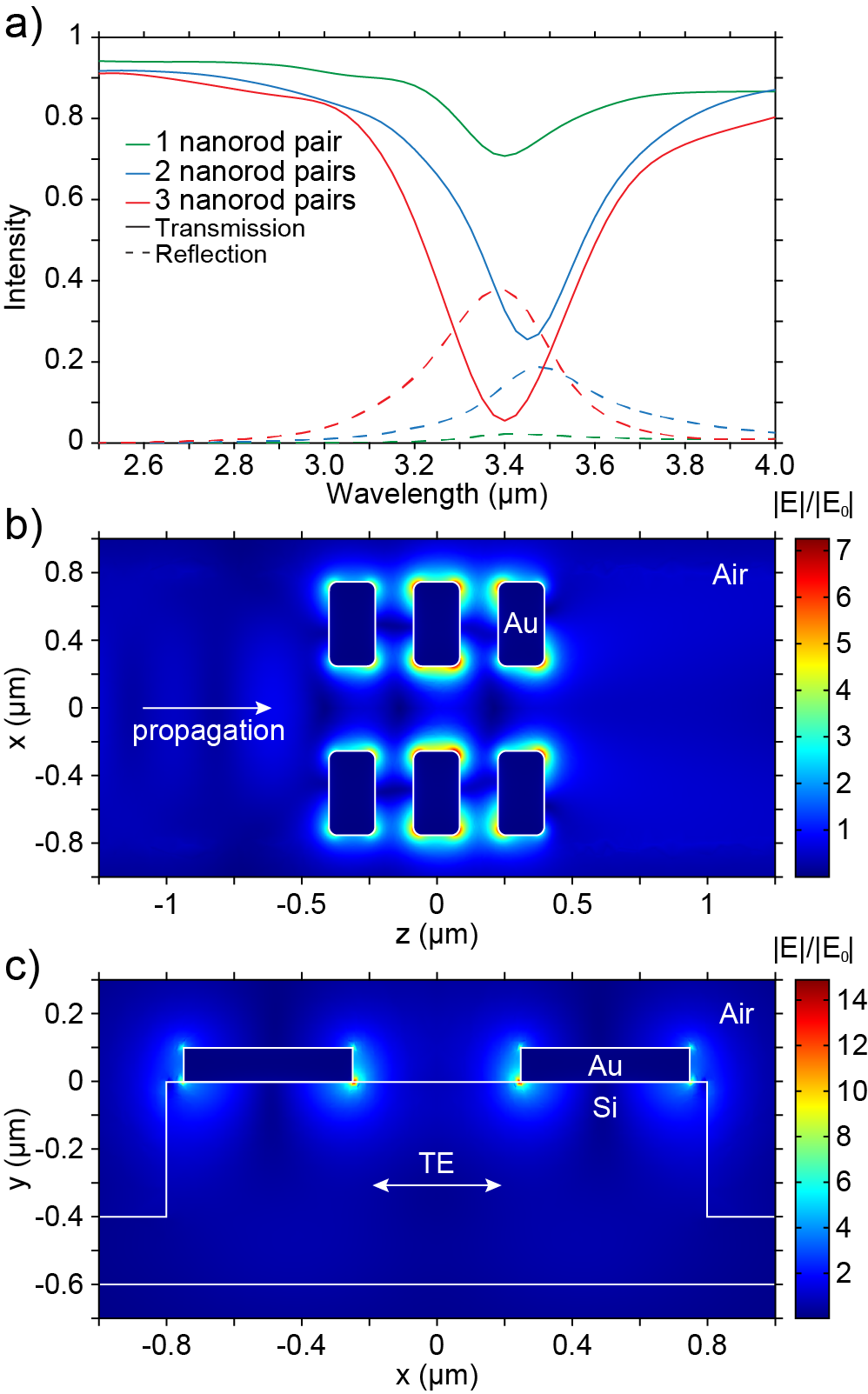
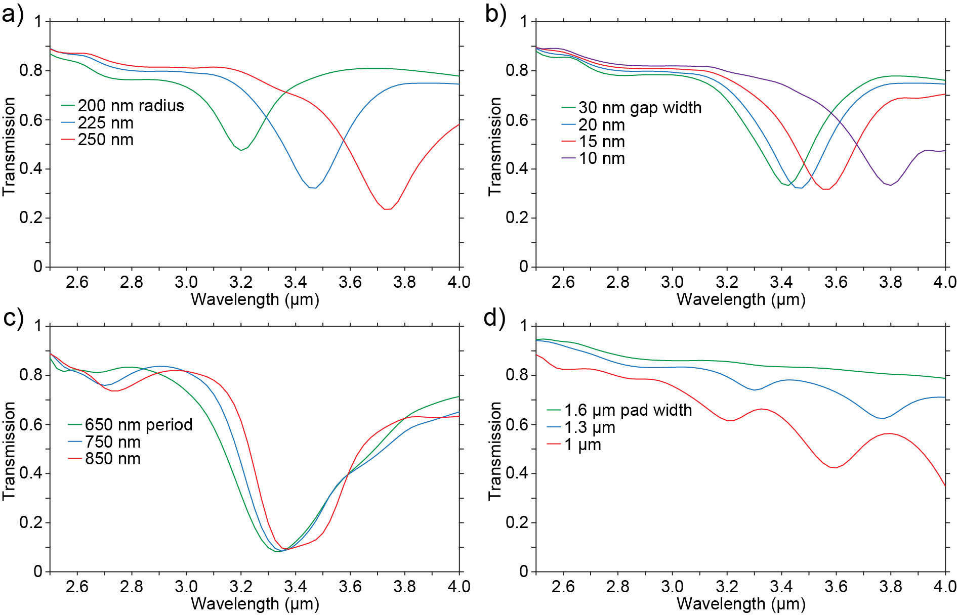
A complementary structure we propose for waveguide-integrated plasmonics are annular apertures with very small gaps (10s of nm), which are also promising for MIR SEIRA applicationsref30 ; ref31 . These structures can support many different resonancesref30 ; ref32 ; ref33 ; ref34 ; ref35 ; ref36 , including a TEM moderef37 ; ref38 that does not exhibit a cut-off, but the most convenient for excitation from a single TE-mode Si waveguide is the TE11-like cutoff resonance. This cutoff resonance can be explained simply as a zeroth-order Fabry-Perot resonance. As the excitation wavelength increases to the cutoff wavelength, the real part of the propagation constant, , decreases to zero, while the imaginary component increases, turning the mode from propagative to evanescent. Examining the transmission intensity for a Fabry-Perot cavity, where are the transmission amplitude coefficients of the cavity ends, are the reflection amplitude coefficients with corresponding phases , and is the thickness, we find that if the reflection phase is negative, it can cancel with and the Fabry-Perot condition is fulfilled, leading to resonant transmission and field enhancement. Since the propagation phase in the cavity is canceled upon reflection at the ends (and ), the field profile is uniform, as seen in Figure 3c. Alternatively, this zeroth-order Fabry-Perot resonance can be considered as an example of epsilon-near-zero (ENZ) phenomenaref39 ; ref40 and the high transmission resulting from ‘super-coupling’. As the radius of the aperture is increased, the resonance red shifts (toward longer wavelengths) and increases the coupling efficiency (Figure 8a). As the gap is decreased, the resonance also red-shifts (Figure 8b), but the strength of the resonance remains approximately the same, suggesting that mode-overlap area is more critical in coupling than the open-area of the aperture.
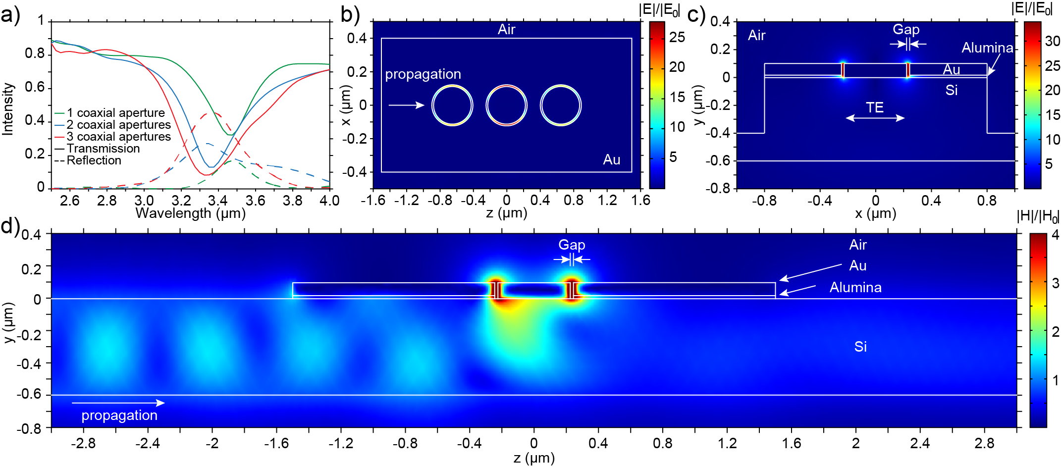
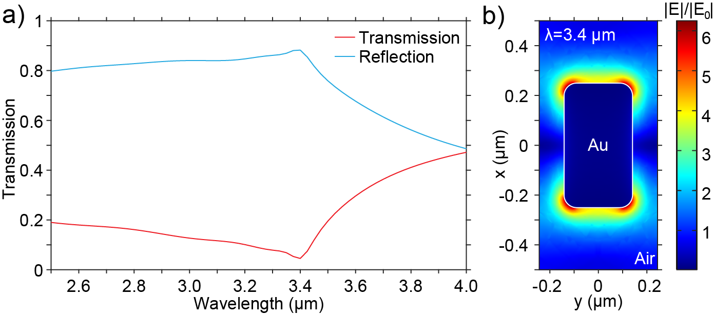
Placing a single aperture on the waveguide with a 20 nm gap, we find coupling efficiencies of 40% around 3.5 m (Figure 3a), much higher than those reported for individual nanorodsref41 . Placing multiple structures on the same gold pad increases the coupling as expected, with little dependence of the periodicity of the devices (Figure 8c). A fabrication method of these structures with open gaps available for the greatest SEIRA signal leverages atomic layer deposition (ALD) of sacrificial Al2O3 layers to define nanometer-wide gaps, a scheme called atomic layer lithographyref30 ; ref42 ; ref43 . In placing this structure on the waveguide, a metallic pad is needed to act as the cladding of the coaxial aperture, which we found to introduce relatively small scattering losses into the signal. Failure to properly design the cladding, however, can lead to quite significant pad resonances (Figure 8d).
III Results and Discussion
To evaluate the SEIRA performance of each of these structures, we simulated the structures with both a uniform 200 nm layer of PMMA and a 2 nm octadecanethiol (ODT) self-assembled monolayer and examined the absorption of the C-H bond bending resonances around 3.4 m. The 200 nm layer of PMMA is intended to probe the entire electric field distribution available for sensing, while the 2 nm layer yield information regarding the confinement of the field to the surface. As can be seen in Figure 4, both nanorods and coaxial nanoapertures yield clear absorption responses of 2% and 7%, respectively, for the 200 nm PMMA layer. With a 2 nm layer of ODT, the normalized absorption for a coaxial nanoaperture is over 0.7%, while absorption in the nanorod case is much less, at just over 0.1%. This is due to the relative resonance modes of each of the structures. For nanorods, a significant portion of the electric field distribution on resonance is contained inside the silicon, and therefore is not available for sensing (Figure 2b), while in etched coaxial nanoapertures, nearly the entire field distribution is available (Figure 3b). This explains some of the intuition of why coaxial nanoapertures in the 200 nm PMMA case yield higher absorption responses. When reducing the analyte thickness to only 2 nm, the metal nanorods yield greatly reduced signals due to the poor field confinement, while coaxial nanoapertures maintain higher absorption levels since the field confinement is essentially defined by the gap size, which is 20 nm in this case.
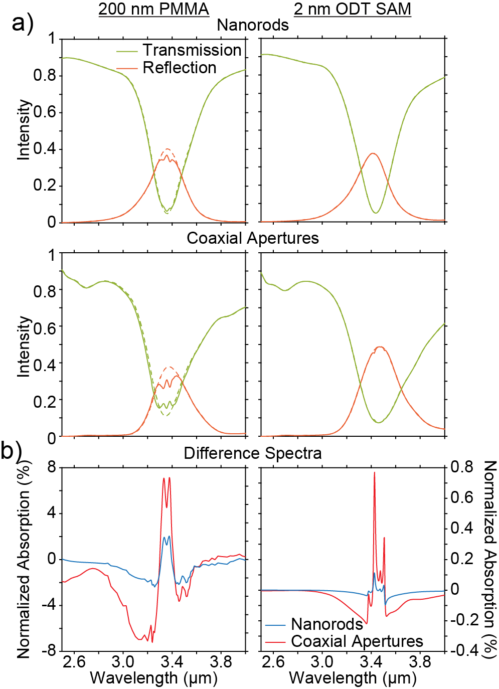
These findings suggest that coaxial nanoapertures generally exhibit higher performance, which is not surprising when taking into account the recent work of Huck, et al.ref44 , which describes why aperture-based structures are often superior to antennas. Essentially, the bulk of the nanorod signal is sourced from the ends of the device, while gaps generally have a more uniform, higher electric field distribution which increases sensitivity to analyte. The gap-defined field distribution in coaxial nanoapertures can be precisely controlled below 10 nm (e.g. by using atomic layer lithography). This allows one to both tailor the field distribution to the sensing analyte and increase the sensitivity of the device per analyte particle. With the devices considered in our work, we also found greater coupling per single resonator when comparing the two resonator designs, important for pushing to low limits of detection.
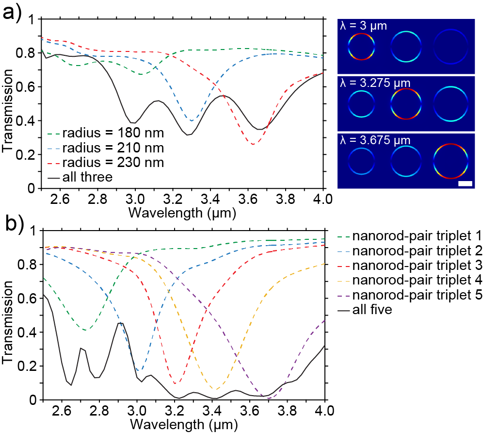
Up to this point, structures with only one geometrical set of parameters have been examined. By placing multiple structures on the same waveguide with varying parameters, it is possible to create very broad resonances. As seen in Figure 5a, coaxial nanoapertures with varying radii can be combined into one small Au pad (3 m long) to create a broadband resonance. Figure 5b contains the spectra simulated for five nanorod-pair triplets placed atop the same waveguide. Many other groups have been interested in creating plasmonic resonators for SEIRA that contain multiple resonances to obtain broad spectra of the analyteref45 . While many of those same structures can still be used here (depending on their polarization sensitivity), by integrating devices serially on the waveguide, the same effect can be shown. While the work here has been targeted for SEIRA near 3 m, the platform can easily be scaled to longer (or shorter) wavelength regimes, such as 6 m, where a wide range of organic molecules have many strong vibrational modes.
IV Conclusion
Waveguide-integrated plasmonics is a growing field with many promising aspects for use in the lab-on-a-chip and photonics communities. While visible/NIR sensing applications of both SERS and refractometric sensing have both been previously demonstrated, in this work we computationally push the devices to the MIR for the application of SEIRA. In comparing gold nanorods and coaxial nanoapertures using simulated PMMA and ODT layers, we find that ring-shaped coaxial nanoapertures, a gap-based device exhibiting super-coupling effects, yields superior performance to nanorods, but both can have 90% absorption in a near diffraction-limited size. Furthermore, using a single coaxial nanoaperture, we find up to 40% of absorption, pushing the bar towards ultrasensitive detections of low-number molecular analytes. While the devices are only theoretically studied here, the fabrication of these devices is achievable, which we plan to demonstrate in a future publication and evaluate real-world performance.
V Methods
Computational modeling was performed using COMSOL Multiphysics in the frequency domain. To decrease simulation time, only half of the geometry was simulated taking advantage of the plane of symmetry parallel to the waveguide while scattering boundary conditions were used perpendicular to the waveguide direction (except for the boundary of symmetry). Perfectly matched layers were used at the ends of the waveguide to increase the accuracy of the simulation. Reflection and transmission measurements were measured across a simulation plane before and after the plasmonic devices. Only the optical power in the fundamental TE modes were included in these calculations. Optical constants for silicon, gold, alumina, PMMA, and ODT were obtained from previous worksref46 ; ref47 ; ref48 ; ref49 ; ref50 .
VI Acknowledgments
This work was supported primarily by the grant from the National Science Foundation (NSF ECCS No. 1610333 to D.Y. and S.-H.O.; NSF ECCS No. 1708768 to C.C. and M.L.); Seagate Technology through the University of Minnesota MINT consortium (D.A.M. and S.- H.O.). D.A.M. also acknowledges support from the NIH Biotechnology Training Grant (T32 GM008347) and Jackie. Computational modeling was carried out in part using resources provided by the University of Minnesota Supercomputing Institute.
References
- (1) Maier, S. A.; Kik, P. G.; Atwater, H. A.; Meltzer, S.; Harel, E.; Koel, B. E.; Requicha, A. A. G. Local Detection of Electromagnetic Energy Transport Below the Diffraction Limit in Metal Nanoparticle Plasmon Waveguides. Nature Mater. 2003, 2, 229-232.
- (2) Barnes, W. L.; Dereux, A.; Ebbesen, T. W. Surface Plasmon Subwavelength Optics. Nature 2003, 424, 824-830.
- (3) Peyskens, F.; Dhakal, A.; Van Dorpe, P.; Le Thomas, N.; Baets, R. Surface Enhanced Raman Spectroscopy Using a Single Mode Nanophotonic-Plasmonic Platform. ACS Photonics 2015, 3, 102-108.
- (4) Oulton, R. F.; Sorger, V. J.; Zentgraf, T.; Ma, R.-M.; Gladden, C.; Dai, L.; Bartal, G.; Zhang, X. Plasmon Lasers at Deep Subwavelength Scale. Nature 2009, 461, 629-632.
- (5) Haffner, C.; Heni, W.; Fedoryshyn, Y.; Niegemann, J.; Melikyan, A.; Elder, D. L.; Baeuerle, B.; Salamin, Y.; Josten, A.; Koch, U.; Hoessbacher, C.; Ducry, F.; Juchli, L.; Emboras, A.; Hillerkuss, D.; Kohl, M.; Dalton, L. R.; Hafner, C.; Leuthold, J. All-Plasmonic Mach–Zehnder Modulator Enabling Optical High-Speed Communication at the Microscale. Nature Photonics 2015, 9, 525-528.
- (6) Vercruysse, D.; Neutens, P.; Lagae, L.; Verellen, N.; Van Dorpe, P. Single Asymmetric Plasmonic Antenna as a Directional Coupler to a Dielectric Waveguide. ACS Photonics 2017, 4, 1398-1402.
- (7) Li, H.; Noh, J. W.; Chen, Y.; Li, M. Enhanced Optical Forces in Integrated Hybrid Plasmonic Waveguides. Opt. Express 2013, 21, 11839-11851.
- (8) Thijssen, R.; Verhagen, E.; Kippenberg, T. J.; Polman, A. Plasmon Nanomechanical Coupling for Nanoscale Transduction. Nano Lett. 2013, 13, 3293-3297.
- (9) Fakonas, J. S.; Lee, H.; Kelaita, Y. A.; Atwater, H. A. Two-Plasmon Quantum Interference. Nature Photonics 2014, 8, 317-320.
- (10) Choo, H.; Kim, M.-K.; Staffaroni, M.; Seok, T. J.; Bokor, J.; Cabrini, S.; Schuck, P. J.; Wu, M. C.; Yablonovitch, E. Nanofocusing in a Metal–Insulator–Metal Gap Plasmon Waveguide with a Three-Dimensional Linear Taper. Nature Photonics 2012, 6, 838-844.
- (11) Nielsen, M. P.; Lafone, L.; Rakovich, A.; Sidiropoulos, T. P. H.; Rahmani, M.; Maier, S. A.; Oulton, R. F. Adiabatic Nanofocusing in Hybrid Gap Plasmon Waveguides on the Silicon-on-Insulator Platform. Nano Lett. 2016, 16, 1410-1414.
- (12) Liu, M.; Yin, X.; Ulin-Avila, E.; Geng, B.; Zentgraf, T.; Ju, L.; Wang, F.; Zhang, X. A Graphene-Based Broadband Optical Modulator. Nature 2011, 474, 64-67.
- (13) Youngblood, N.; Chen, C.; Koester, S. J.; Li, M. Waveguide-Integrated Black Phosphorus Photodetector with High Responsivity and Low Dark Current. Nature Photonics 2015, 9, 247-252.
- (14) Chen, C.; Youngblood, N.; Peng, R.; Yoo, D.; Mohr, D. A.; Johnson, T. W.; Oh, S.-H.; Li, M. Three-Dimensional Integration of Black Phosphorus Photodetector with Silicon Photonics and Nanoplasmonics. Nano Lett. 2017, 17, 985-991.
- (15) Février, M.; Gogol, P.; Barbillon, G.; Aassime, A.; Mégy, R.; Bartenlian, B.; Lourtioz, J.-M.; Dagens, B. Integration of Short Gold Nanoparticles Chain on SOI Waveguide Toward Compact Integrated Bio-Sensors. Opt. Express 2012, 20, 17402.
- (16) Maier, S. Plasmonics: Fundamentals and Applications; Springer: New York, NY, 2007.
- (17) Law, S.; Podolskiy, V.; Wasserman, D. Towards Nano-Scale Photonics with Micro-Scale Photons: the Opportunities and Challenges of Mid-Infrared Plasmonics. Nanophotonics 2013, 2, 103-130.
- (18) Rodrigo, D.; Limaj, O.; Janner, D.; Etezadi, D.; de Abajo, F. J. G.; Pruneri, V.; Altug, H. Mid-Infrared Plasmonic Biosensing with Graphene. Science 2015, 349, 165-168.
- (19) Low, T.; Avouris, P. Graphene Plasmonics for Terahertz to Mid-Infrared Applications. ACS Nano 2014, 8, 1086-1101.
- (20) Schnell, M.; Alonso-Gonzalez, P.; Arzubiaga, L.; Casanova, F.; Hueso, L. E.; Chuvilin, A.; Hillenbrand, R. Nanofocusing of Mid-Infrared Energy with Tapered Transmission Lines. Nature Photonics 2011, 5, 283-287.
- (21) Osawa, M. Surface-Enhanced Infrared Absorption. Topics Appl. Phys. 2001, 81, 163-187.
- (22) Adato, R.; Yanik, A. A.; Amsden, J. J.; Kaplan, D. L.; Omenetto, F. G.; Hong, M. K.; Erramilli, S.; Altug, H. Ultra-Sensitive Vibrational Spectroscopy of Protein Monolayers with Plasmonic Nanoantenna Arrays. Proc. Natl. Acad. Sci. USA 2009, 106, 19227-19232.
- (23) Wu, C.; Khanikaev, A. B.; Adato, R.; Arju, N.; Yanik, A. A.; Altug, H.; Shvets, G. Fano-Resonant Asymmetric Metamaterials for Ultrasensitive Spectroscopy and Identification of Molecular Monolayers. Nature Mater. 2012, 11, 69-75.
- (24) Brown, L. V.; Zhao, K.; King, N.; Sobhani, H.; Nordlander, P.; Halas, N. J. Surface-Enhanced Infrared Absorption Using Individual Cross Antennas Tailored to Chemical Moieties. J. Am. Chem. Soc. 2013, 135, 3688-3695.
- (25) Brown, L. V.; Yang, X.; Zhao, K.; Zheng, B. Y.; Nordlander, P.; Halas, N. J. Fan-Shaped Gold Nanoantennas Above Reflective Substrates for Surface-Enhanced Infrared Absorption (SEIRA). Nano Lett. 2015, 15, 1272-1280.
- (26) Huck, C.; Neubrech, F.; Vogt, J.; Toma, A.; Gerbert, D.; Katzmann, J.; H’́artling, T.; Pucci, A. Surface-Enhanced Infrared Spectroscopy Using Nanometer-Sized Gaps. ACS Nano 2014, 8, 4908-4914.
- (27) Chen, X.; Cirací, C.; Smith, D. R.; Oh, S.-H. Nanogap-Enhanced Infrared Spectroscopy with Template-Stripped Wafer-Scale Arrays of Buried Plasmonic Cavities. Nano Lett. 2015, 15, 107-113.
- (28) Neubrech, F.; Huck, C.; Weber, K.; Pucci, A.; Giessen, H. Surface-Enhanced Infrared Spectroscopy Using Resonant Nanoantennas. Chem. Rev. 2017, 117, 5110-5145.
- (29) Chen, Y.; Lin, H.; Hu, J.; Li, M. Heterogeneously Integrated Silicon Photonics for the Mid-Infrared and Spectroscopic Sensing. ACS Nano 2014, 8, 6955-6961.
- (30) Yoo, D.; Nguyen, N.-C.; Martín-Moreno, L.; Mohr, D. A.; Carretero-Palacios, S.; Shaver, J.; Peraire, J.; Ebbesen, T. W.; Oh, S.-H. High-Throughput Fabrication of Resonant Metamaterials with Ultrasmall Coaxial Apertures via Atomic Layer Lithography. Nano Lett. 2016, 16, 2040-2046.
- (31) Yoo, D.; Mohr, D. A.; Vidal-Codina, F.; John-Herpin, A.; Jo, M.; Kim, S.; Matson, J.; Caldwell, J. D.; Jeon, H.; Nguyen, N.-C.; Martín-Moreno, L.; Peraire, J.; Altug, H.; Oh, S.-H. High-Contrast Infrared Absorption Spectroscopy via Mass-Produced Coaxial Zero-Mode Resonators with Sub-10 Nm Gaps. Nano Lett. 2018, 18, 1930-1936.
- (32) Baida, F. I.; Van Labeke, D. Light Transmission by Subwavelength Annular Aperture Arrays in Metallic Films. Opt. Commun. 2002, 209, 17-22.
- (33) Fan, W.; Zhang, S.; Minhas, B.; Malloy, K. J.; Brueck, S. R. J. Enhanced Infrared Transmission Through Subwavelength Coaxial Metallic Arrays. Phys. Rev. Lett. 2005, 94, 033902.
- (34) Orbons, S. M.; Roberts, A. Resonance and Extraordinary Transmission in Annular Aperture Arrays. Opt. Express 2006, 14, 12623-12628.
- (35) de Waele, R.; Burgos, S. P.; Polman, A.; Atwater, H. A. Plasmon Dispersion in Coaxial Waveguides From Single-Cavity Optical Transmission Measurements. Nano Lett. 2009, 9, 2832-2837.
- (36) Catrysse, P. B.; Fan, S. Understanding the Dispersion of Coaxial Plasmonic Structures Through a Connection with the Planar Metal-Insulator-Metal Geometry. Appl. Phys. Lett. 2009, 94, 231111.
- (37) Baida, F. I.; Belkhir, A.; Van Labeke, D.; Lamrous, O. Subwavelength Metallic Coaxial Waveguides in the Optical Range: Role of the Plasmonic Modes. Phys. Rev. B 2006, 74, 205419.
- (38) Li, D.; Gordon, R. Electromagnetic Transmission Resonances for a Single Annular Aperture in a Metal Plate. Phys. Rev. A 2010, 82, 041801(R).
- (39) Silveirinha, M.; Engheta, N. Theory of Supercoupling, Squeezing Wave Energy, and Field Confinement in Narrow Channels and Tight Bends Using -Near-Zero Metamaterials. Phys. Rev. Lett. 2007, 76, 245109.
- (40) Argyropoulos, C.; Chen, P.-Y.; D’Aguanno, G.; Engheta, N.; Alù, A. Boosting Optical Nonlinearities in -Near-Zero Plasmonic Channels. Phys. Rev. B 2012, 85, 045129.
- (41) Espinosa-Soria, A.; Martínez, A.; Griol, A. Experimental Measurement of Plasmonic Nanostructures Embedded in Silicon Waveguide Gaps. Opt. Express 2016, 24, 9592-9601.
- (42) Im, H.; Bantz, K. C.; Lindquist, N. C.; Haynes, C. L.; Oh, S.-H. Vertically Oriented Sub-10-nm Plasmonic Nanogap Arrays. Nano Lett. 2010, 10, 2231-2236.
- (43) Chen, X.; Park, H.-R.; Pelton, M.; Piao, X.; Lindquist, N. C.; Im, H.; Kim, Y. J.; Ahn, J. S.; Ahn, K. J.; Park, N.; Kim, D.-S.; Oh, S.-H. Atomic Layer Lithography of Wafer-Scale Nanogap Arrays for Extreme Confinement of Electromagnetic Waves. Nature Commun. 2013, 4, 2361.
- (44) Huck, C.; Vogt, J.; Sendner, M.; Hengstler, D.; Neubrech, F.; Pucci, A. Plasmonic Enhancement of Infrared Vibrational Signals: Nanoslits Versus Nanorods. ACS Photonics 2015, 2, 1489-1497.
- (45) Limaj, O.; Etezadi, D.; Wittenberg, N. J.; Rodrigo, D.; Yoo, D.; Oh, S.-H.; Altug, H. Infrared Plasmonic Biosensor for Real-Time and Label-Free Monitoring of Lipid Membranes. Nano Lett. 2016, 16, 1502-1508.
- (46) Chandler-Horowitz, D.; Amirtharaj, P. M. High-Accuracy, Midinfrared (450 4000 ) Refractive Index Values of Silicon. J. Appl. Phys. 2005, 97, 123526.
- (47) Olmon, R. L.; Slovick, B.; Johnson, T. W.; Shelton, D.; Oh, S.-H.; Boreman, G. D.; Raschke, M. B. Optical Dielectric Function of Gold. Phys. Rev. B 2012, 86, 235147.
- (48) Kischkat, J.; Peters, S.; Gruska, B.; Semtsiv, M.; Chashnikova, M.; Klinkm’́uller, M.; Fedosenko, O.; Machulik, S.; Aleksandrova, A.; Monastyrskyi, G.; Flores, Y.; Ted Masselink, W. Mid-Infrared Optical Properties of Thin Films of Aluminum Oxide, Titanium Dioxide, Silicon Dioxide, Aluminum Nitride, and Silicon Nitride. Appl. Opt. 2012, 51, 6789.
- (49) Graf, R. T.; Koenig, J. L.; Ishida, H. Optical Constant Determination of Thin Polymer Films in the Infrared:. Appl. Spectrosc. 1985, 39, 405-408.
- (50) Hu, Z. G.; Prunici, P.; Patzner, P.; Hess, P. Infrared Spectroscopic Ellipsometry of N-Alkylthiol (C5-C18) Self-Assembled Monolayers on Gold. J. Phys. Chem. B 2006, 110, 14824-14831.
Appendix A Supporting Information