Electrically Benign Defect Behavior in Zinc Tin Nitride Revealed from First Principles
Abstract
Zinc tin nitride (ZnSnN2) is attracting growing interest as a non-toxic and earth-abundant photoabsorber for thin-film photovoltaics. Carrier transport in ZnSnN2 and consequently cell performance are strongly affected by point defects with deep levels acting as carrier recombination centers. In this study, the point defects in ZnSnN2 are revisited by careful first-principles modeling based on recent experimental and theoretical findings. It is shown that ZnSnN2 does not have low-energy defects with deep levels, in contrast to previously reported results. Therefore, ZnSnN2 is more promising as a photoabsorber material than formerly considered.
ZnSnN2 has a wurtzite-derived structure with a minimum gap of 1.4 eV in its direct-type band structure Lahourcade et al. (2013); Lany et al. (2017), which is very close to the best place of the Shockley–Queisser limit of 1.34 eV Shockley and Queisser (1961). In addition, the electron effective mass of 0.17m0 and its heavy-hole mass of 2.00m0 are comparable or even superior to those of GaN (Fig. S2, Supplemental Material 111See Supplemental Material at [URL will be inserted by publisher] for details of bulk and defect properties in ZnSnN2.) Hinuma et al. (2016). However, there are several fundamentally and technologically important issues regarding the use of ZnSnN2 as a light absorption layer that need to be assessed: (i) Point defect properties. It is necessary to identify any point defects with deep levels, because they trap electrons and/or holes and cause carrier recombination, leading to loss of cell efficiency. (ii) Unintentional n-type doping. The carrier-electron concentration generally unintentionally increases up to 1021 cm-3 in ZnSnN2 as well as other narrow gap nitrides like InN, Zn3N2, and ScN Wu et al. (2004); Kumagai et al. (2017, 2018). For solar cell applications, the carrier-electron concentration needs to be lowered to around 1016-1018 cm-3. Besides, the photoabsorption onset is increased up to 2.4 eV Lahourcade et al. (2013); Feldberg et al. (2013); Veal et al. (2015) because of the Burstein–Moss (BM) shift Burstein (1954); Moss (1954), which has raised considerable controversy regarding the fundamental gap of ZnSnN2. The BM shift is also directly related to the formation of donor-type point defects. Understanding the point-defect properties of ZnSnN2 is thus imperative to optimize its performance in photovoltaics.
Chen et al. Chen et al. (2014) investigated native point defects and oxygen impurities in ZnSnN2 with an ordered orthorhombic structure. They reported that Sn-on-Zn antisite (SnZn) and O-on-N (ON) substitutional defects have low formation energies with deep donor levels, and thus do not cause the BM shift in ZnSnN2. However, given recent experimental and theoretical findings Lahourcade et al. (2013); Lany et al. (2017); Feldberg et al. (2013); Veal et al. (2015); Fioretti et al. (2015); Quayle et al. (2015); Fioretti et al. (2017), this conclusion needs to be reviewed. This motivated us to reevaluate point defects in ZnSnN2 including as-yet-uninvestigated hydrogen impurities. Our results show that all the defects with deep levels are very high in energy and the abundant defects act as shallow donors. Considering these favorable defect properties together with its appropriate band gap and high absorption coefficient, ZnSnN2 is a promising photoabsorber for thin-film photovoltaics.
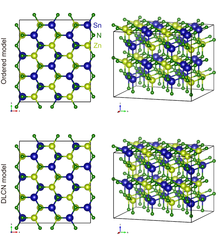
Our theoretical investigation of the point defects in ZnSnN2 was performed for the Pna21 orthorhombic structure with 16 atoms in the unit cell, referred to here as the ordered model. However, a certain level of disorder in the cation sublattice appears to be unavoidable because of the very low cation order–disorder transition temperature Lany et al. (2017). At low temperature, the disordered phase strictly retains the local charge neutrality, in which each N atom is necessarily coordinated by two Sn and two Zn atoms. We refer to such a structure as the disordered structure with local charge neutrality (DLCN). It has been reported that the electronic structure of the DLCN is almost identical to that of the ordered structure Lany et al. (2017); Quayle et al. (2015). Thus, the DLCN should be ideal as a photoabsorber, unless its defects are detrimental to its efficiency. We thus considered both ordered and DLCN models in our defect calculations. Note that cation disorder breaking the local charge neutrality occurs at very high temperature ( 1750 K Lany et al. (2017)). Some authors have used special quasirandom structures (SQS) to examine the behavior of the cation disordered phase Feldberg et al. (2013); Veal et al. (2015). Such a fully random cation disordered model is not appropriate for ZnSnN2 because its typical growth temperature is much lower than 1750 K Lahourcade et al. (2013); Feldberg et al. (2013); Veal et al. (2015); Fioretti et al. (2015, 2017). Besides, when the charge neutrality is broken, a high concentration of Zn-on-Sn (ZnSn) defects is introduced. This situation should be avoided for photovoltaic applications because ZnSn defects give rise to deep levels, as discussed later.
Figure 1 shows the two models used to evaluate defect formation energies. The DLCN model was generated by Monte Carlo simulated annealing of a 128-atom orthorhombic supercell. The DLCN model shown in Fig. 1 belongs to space group Pna21 and consists of a 32-atom unit cell, consistent with that reported elsewhere Lany et al. (2017). Note that there are infinite possible configurations for the DLCN models when different cell sizes are considered; however, within the 128-atom supercell, we found only one configuration owing to the strong geometrical constraint of the local charge neutrality.
First, we discuss the band gap of ZnSnN2 because it is a central controversy in the research of this material. As the carrier-electron concentration increases, the photoabsorption onset also increases due to the BM shift. The blueshift estimated from the Heyd-Scuseria-Ernzerhof (HSE06) hybrid functional calculations is 0.2-2.3 eV when the carrier-electron concentration is 1018-1021 cm-3 observed in experiments Lahourcade et al. (2013); Feldberg et al. (2013); Veal et al. (2015) (Fig. S6, Supplemental Material 11footnotemark: 1). Thus, larger experimental band gaps than 1.4 eV could be attributed to the BM shift, as has also been discussed by Lahourcade et al. Lahourcade et al. (2013) Second, the band gaps of fully cation disordered systems are ill-defined because the minimum gap decreases as the model size increases Seko and Tanaka (2015). In the case of ZnSnN2, the density of states tends to continuously develop within the band gap when N atoms are coordinated by three or four Sn or Zn atoms, as discussed later. Note that this does not necessarily indicate metallic behavior because the defect states are discontinuous in real space. Refer to the Supplemental Material for a more detailed discussion considering SQS (Fig. S8 11footnotemark: 1).
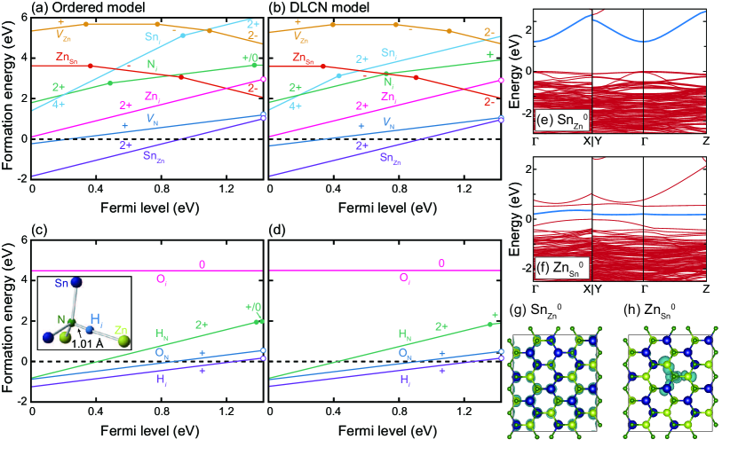
We now discuss the energetics of point defects in ZnSnN2. To investigate the site dependency in the DLCN model, we conducted over 300 point-defect calculations using the modified Perdew–Burke–Ernzerhof generalized gradient approximation tuned for solids (PBEsol-GGA) Perdew et al. (2008). We confirmed that most of the defect species show only negligible site dependencies in energy, while the interstitial defects do relatively large ones probably due to the difference in neighboring cation configurations at the octahedral sites (Fig. S9, Supplemental Material 11footnotemark: 1). Thus, we performed HSE06 calculations for a few configurations with lower energies in PBEsol calculations for each defect and show only the results of the lowest energy configurations hereafter. Figure 2 shows the resultant formation energies of the native defects as well as hydrogen and oxygen impurities, which are ubiquitous in nitrides. Since ZnSnN2 is only slightly stable (f = -0.015 eV/atom) compared to Zn metal, Sn metal, and N2 molecules using HSE06, the growth condition does not largely affect the formation energies under the equilibrium condition. Therefore, here, the chemical potentials of constituent elements are set at the point where Zn and Sn metals equilibrate with ZnSnN2. As mentioned above, the standard HSE06 functional used in this study yielded a direct gap of 1.4 eV. In the study by Chen et al., the Fock exchange ratio was increased to reproduce a reported experimental gap of 2.0 eV Lahourcade et al. (2013) although one of the authors attributed this larger gap to the BM shift and stated that the fundamental gap is about 1.4 eV Lahourcade et al. (2013).
Before discussing the results, let us consider the technical details that can alter conclusions even qualitatively. Chen et al. Chen et al. (2014) did not consider the finite cell-size effects when calculating defect formation energies and the reciprocal space sampling was performed using only the point. According to our calculated cell-size dependencies, a maximum error of 0.72 eV arises when the 128-atom supercell is used with these settings. In this study, we decreased these errors using the extended Freysoldt–Neugebauer–Van de Walle (FNV) corrections Kumagai and Oba (2014); Freysoldt et al. (2009) and 222 Monkhorst–Pack -point sampling for the 128-atom supercell. Consequently, the errors based on our test calculations are less than 0.06 eV. In the case of defects exhibiting hydrogenic states, a huge supercell including tens of thousands of atoms is usually required to avoid overlap between widespread defect orbitals Zhang et al. (2013). When using the 128-atom supercell in ZnSnN2, the thermodynamic transition levels of such defects are overestimated by a few tenths of eV because of the defect–defect interaction (see Fig. S10, Supplemental Material 11footnotemark: 1). Therefore, we discuss the transition levels associated with hydrogenic states only qualitatively.
Figures 2(a–d) reveals that there is little difference between the defect formation energies of the ordered and DLCN models, which means that not only the bulk properties but also the point-defect properties are strongly correlated with its immediate coordination environment. This conclusion would also hold for similar cation disordered systems such as ZnSnP2 Kumagai et al. (2014); Scanlon and Walsh (2012) and ZnGeN2 Skachkov et al. (2016) if the local charge neutrality is preserved. It is also notable that defects and impurities that show low formation energies simultaneously with deep levels do not exist when the Fermi level is located within the band gap. This is in stark contrast to the conclusion of a previous study Chen et al. (2014) that the Zn interstitial (Zni), SnZn, nitrogen vacancy (), and ON have deep defect levels and act as carrier recombination centers. This discrepancy is mainly caused by the aforementioned difference in the treatment of the cell-size corrections and -point sampling.
As shown in Figures 2(e) and (g), Sn exhibits an occupied hydrogenic state, namely perturbed host state, while the localized defect state is not confirmed near the conduction-band minimum (CBM), which is different from the results by Chen et al. Chen et al. (2014) Therefore, SnZn is a dominant shallow donor among the native defects. Its formation energy becomes zero at the Fermi level being 0.9 eV above the valence-band maximum (VBM), which hinders -type conversion even with acceptor doping. is a single shallow donor in the entire Fermi level range, but has a higher formation energy than that of SnZn. In contrast, acceptor-type defect ZnSn forms two deep transition levels between the 0, -1, and -2 charge states. Indeed, as seen in Figures 2(f) and (h), Zn shows two deep localized defect states within the band gap. However, the formation energy of ZnSn is rather high when the Fermi level is within the band gap. The other defects, namely, Zn vacancy (), Sn vacancy (), Sn interstitial (Sni), and N interstitial (Ni), create deep levels but have very high formation energies. It is also noteworthy that Sn does not become a DX center ( + Sni) in our calculations unlike ZnSnP2 Kumagai et al. (2014) probably because of the high formation energies of and Sni and/or the difference in crystal structures.
Oxygen and hydrogen impurities are energetically favorable at the N sites (ON) and interstitial sites (Hi), respectively. These impurities also act as single shallow donors and exhibit low formation energies even when the Fermi level is at the CBM. Orbital analyses indicated that their donor electrons are located at the perturbed conduction bands. Therefore, these impurities should primarily cause the BM shift. However, in the previous study Chen et al. (2014), the origin of the high carrier-electron concentration was attributed to the defect band originating from SnZn and ON, which is different from our results. Hi forms an N-H bond (1.01 Å) between N and Zn atom, as commonly observed for nitrides. We also found that anionic hydrogen H is not stabilized even when the Fermi level is located at 1 eV above the CBM in ZnSnN2 (see Fig. S12, Supplemental Material 11footnotemark: 1), unlike in GaN Neugebauer and Van de Walle (1995).
Recently, Fioretti et al. Fioretti et al. (2017) showed that annealing Zn-rich Zn1+xSn1-xN2 grown in a hydrogen atmosphere decreased its carrier-electron concentration to 4 1016 cm-3. They explained this observation from the viewpoint of hydrogen passivation of acceptors, i.e., ZnSn + Hi in Zn1+xSn1-xN2 during growth, which lowers the driving force for the formation of other unintentional donors. Indeed, our results indicate that complexing with hydrogen is exothermic and drastically decreases the formation energy of acceptor ZnSn (Fig. S13 11footnotemark: 1); the binding energy, i.e., the energy change from isolated ZnSn-2 and H to (ZnSn + Hi)- is -1.43 eV and that from isolated H and (ZnSn + Hi)- to (ZnSn + 2Hi)0 is -0.73 eV. Therefore, abundant ZnSn antisites are easily introduced by hydrogen passivation as discussed by Fioretti et al. We, however, emphasize that ZnSn antisites, which generate deep transition levels and trap minority carrier holes, persist even after removing the passivating hydrogen by post-deposition annealing. Moreover, the determination of the intrinsic band gap would be inhibited by the optical absorption related to the defect band.
Here, we propose an alternative route to achieving ZnSnN2 with lower carrier-electron concentration. In the above discussion, the chemical potentials were set at a point where the Zn and Sn metals equilibrate with ZnSnN2. However, recent growth techniques such as reactive sputtering can be used to raise the chemical potential of N () by up to +1 eV/N from that of an inactive N2 molecule Sun et al. (2017). Consequently, metastable nitrides can be synthesized. A notable example is Cu3N, in which needs to be at least +1.04 eV higher than that of an N2 molecule Sun et al. (2017). When was increased to this value, we can use more advantageous condition for lowring the carrier-electron concentration. Figure 3 shows the formation energies of native defects and oxygen impurity under = +1 eV/N and Zn-rich (Sn-poor) condition (see Fig. S16 for details 11footnotemark: 1). The equilibrium Fermi level is located at the 0.70 eV from the CBM at 600 K which assumes synthesis temperature of ZnSnN2 Feldberg et al. (2013); Fioretti et al. (2015). In this situation, all the defect concentrations are less than 1014 cm-3 and corresponding carrier concentration is =1.9 1014 cm-3. One might expect that -type conversion by acceptor doping is plausible in this condition as all the donor-type defects compensating holes are high in energy. Therefore, we performed the extensive calculations for impurities Li, Na, K, Cu, and C using HSE06. (see Fig. S17, Supplemental Material 11footnotemark: 1) As a result, however, we found that none of them act as effective acceptor dopants for ZnSnN2 because of deep acceptor levels or incorporation into interstitial sites. Thus, -type conversion in ZnSnN2 seems very difficult as previously considered even if compensating donor-type defects are sufficiently suppressed as in Fig. 3. 222Note that Wang et al. previously investigated Li-, Na-, and K-on-Zn substitution as acceptors for ZnSnN2, and concluded that Li-on-Zn substitution acts as a shallow acceptor Wang et al. (2017). However, their study did not calculate the interstitial dopants which act as donors unlike our study.
Methods. First-principles calculations were performed using the projector augmented wave (PAW) method Blchl (1994); Kresse and Joubert (1999) as implemented in VASP Kresse and Furthmller (1996). The PBEsol-GGA was used to calculate the total energies of various DLCN models and SQS with different sizes, and to check the site and cell-size dependencies of defect formation energies. The HSE06 hybrid functional Heyd et al. (2006); Krukau et al. (2006) with standard parameters was used for the calculations of the band structure, density of states, and defect formation energies. The plane-wave cutoff energy was set to 550 eV for the lattice relaxation of the ordered and DLCN models without defects and 400 eV for the other calculations with fixed lattice constants. The residual forces were converged to less than 0.01 and 0.04 eV/Å for the calculations without and with defects, respectively. Spin polarization was considered for all the defect calculations using HSE06.
The formation energy of a point defect was calculated as Kumagai and Oba (2014)
| (1) | |||||
where and are the total energies of the supercell with defect in charge state and the supercell without a defect, respectively. is the number of removed ( 0) or added ( 0) -type atoms and is the chemical potential representing the growth conditions. The referenced competing phases used were hexagonal Zn, cubic Sn, wurtzite ZnO, and N2 and H2 molecules. is the energy level of the VBM, and is the Fermi level () with respect to . Therefore, . corresponds to the correction energy for a finite supercell size error associated with spurious electrostatic interactions between charged defects. We used our extended FNV correction scheme Kumagai and Oba (2014) in the calculations. More computational details are described in the Supplemental Material. 11footnotemark: 1
Both DLCN and SQS models were generated by Monte Carlo simulated annealing using in-house and CLUPAN codes Seko et al. (2009), respectively (see Fig. S5, Supplemental Material, for more details 11footnotemark: 1).
Conclusions. We theoretically revisited the point defects in ZnSnN2 by realistic modeling of its disordered phase with the local charge neutrality. Our calculations revealed that the ordered and DLCN models exhibited nearly the same stability, volumes, electronic structures, and even point-defect properties, indicating these properties are determined mainly by the immediate coordination environment. It was also found that low-energy defects with deep levels are absent in ZnSnN2 and, therefore, there is less carrier recombination caused by point defects than thought previously. Furthermore, a possible route to ZnSnN2 with lower carrier-electron concentration using non-equilibrium growth techniques was proposed. Our study has unveiled the further potential of ZnSnN2 as a photoabsorber in thin-film photovoltaics.
Acknowledgements. This work was supported by the MEXT Elements Strategy Initiative to Form Core Research Center, Grants-in-Aid for Young Scientists A (Grant No. 15H05541) and Scientific Research A (Grant No. 17H01318) from JSPS, and PRESTO (JPMJPR16N4), and Support Program for Starting Up Innovation Hub MI2I from JST, Japan. The computing resources of ACCMS at Kyoto University were used for a part of this work.
References
- Lahourcade et al. (2013) L. Lahourcade, N. C. Coronel, K. T. Delaney, S. K. Shukla, N. A. Spaldin, and H. A. Atwater, “Structural and optoelectronic characterization of rf sputtered ZnSnN2,” Advanced Materials 25, 2562 (2013).
- Lany et al. (2017) S. Lany, A. N. Fioretti, P. P. Zawadzki, L. T. Schelhas, E. S. Toberer, A. Zakutayev, and A. C. Tamboli, “Monte carlo simulations of disorder in and the effects on the electronic structure,” Phys. Rev. Materials 1, 035401 (2017).
- Shockley and Queisser (1961) W. Shockley and H. J. Queisser, “Detailed balance limit of efficiency of p‐n junction solar cells,” Journal of Applied Physics 32, 510 (1961).
- Note (1) See Supplemental Material at [URL will be inserted by publisher] for details of bulk and defect properties in ZnSnN2.
- Hinuma et al. (2016) Y. Hinuma, T. Hatakeyama, Y. Kumagai, L. A. Burton, H. Sato, Y. Muraba, S. Iimura, H. Hiramatsu, I. Tanaka, H. Hosono, and F. Oba, “Discovery of earth-abundant nitride semiconductors by computational screening and high-pressure synthesis,” Nature Communications 7, 11962 (2016).
- Wu et al. (2004) J. Wu, W. Walukiewicz, S. X. Li, R. Armitage, J. C. Ho, E. R. Weber, E. E. Haller, H. Lu, W. J. Schaff, A. Barcz, and R. Jakiela, “Effects of electron concentration on the optical absorption edge of InN,” Applied Physics Letters 84, 2805 (2004).
- Kumagai et al. (2017) Y. Kumagai, K. Harada, H. Akamatsu, K. Matsuzaki, and F. Oba, “Carrier-Induced Band-Gap Variation and Point Defects in from First Principles,” Phys. Rev. Applied 8, 014015 (2017).
- Kumagai et al. (2018) Y. Kumagai, N. Tsunoda, and F. Oba, “Point defects and -type doping in ScN from first principles,” Phys. Rev. Applied 9, 034019 (2018).
- Feldberg et al. (2013) N. Feldberg, J. D. Aldous, W. M. Linhart, L. J. Phillips, K. Durose, P. A. Stampe, R. J. Kennedy, D. O. Scanlon, G. Vardar, R. L. F. III, T. Y. Jen, R. S. Goldman, T. D. Veal, and S. M. Durbin, “Growth, disorder, and physical properties of ZnSnN2,” Applied Physics Letters 103, 042109 (2013).
- Veal et al. (2015) T. D. Veal, N. Feldberg, N. F. Quackenbush, W. M. Linhart, D. O. Scanlon, L. F. J. Piper, and S. M. Durbin, “Band gap dependence on cation disorder in ZnSnN2 solar absorber,” Advanced Energy Materials 5, 1501462 (2015), 1501462.
- Burstein (1954) E. Burstein, “Anomalous Optical Absorption Limit in InSb,” Phys. Rev. 93, 632 (1954).
- Moss (1954) T. S. Moss, “The interpretation of the properties of indium antimonide,” Proceedings of the Physical Society. Section B 67, 775 (1954).
- Chen et al. (2014) S. Chen, P. Narang, H. A. Atwater, and L.-W. Wang, “Phase stability and defect physics of a ternary ZnSnN2 semiconductor: First principles insights,” Advanced Materials 26, 311 (2014).
- Fioretti et al. (2015) A. N. Fioretti, A. Zakutayev, H. Moutinho, C. Melamed, J. D. Perkins, A. G. Norman, M. Al-Jassim, E. S. Toberer, and A. C. Tamboli, “Combinatorial insights into doping control and transport properties of zinc tin nitride,” J. Mater. Chem. C 3, 11017 (2015).
- Quayle et al. (2015) P. C. Quayle, E. W. Blanton, A. Punya, G. T. Junno, K. He, L. Han, H. Zhao, J. Shan, W. R. L. Lambrecht, and K. Kash, “Charge-neutral disorder and polytypes in heterovalent wurtzite-based ternary semiconductors: The importance of the octet rule,” Phys. Rev. B 91, 205207 (2015).
- Fioretti et al. (2017) A. N. Fioretti, A. Stokes, M. R. Young, B. Gorman, E. S. Toberer, A. C. Tamboli, and A. Zakutayev, “Effects of hydrogen on acceptor activation in ternary nitride semiconductors,” Advanced Electronic Materials 3, 1600544 (2017), 1600544.
- Seko and Tanaka (2015) A. Seko and I. Tanaka, “Special quasirandom structure in heterovalent ionic systems,” Phys. Rev. B 91, 024106 (2015).
- Perdew et al. (2008) J. P. Perdew, A. Ruzsinszky, G. I. Csonka, O. A. Vydrov, G. E. Scuseria, L. A. Constantin, X. Zhou, and K. Burke, “Restoring the density-gradient expansion for exchange in solids and surfaces,” Phys. Rev. Lett. 100, 136406 (2008).
- Kumagai and Oba (2014) Y. Kumagai and F. Oba, “Electrostatics-based finite-size corrections for first-principles point defect calculations,” Phys. Rev. B 89, 195205 (2014).
- Freysoldt et al. (2009) C. Freysoldt, J. Neugebauer, and C. G. Van de Walle, “Fully Ab Initio finite-size corrections for charged-defect supercell calculations,” Phys. Rev. Lett. 102, 016402 (2009).
- Zhang et al. (2013) G. Zhang, A. Canning, N. Grønbech-Jensen, S. Derenzo, and L.-W. Wang, “Shallow impurity level calculations in semiconductors using ab initio methods,” Phys. Rev. Lett. 110, 166404 (2013).
- Kumagai et al. (2014) Y. Kumagai, M. Choi, Y. Nose, and F. Oba, “First-principles study of point defects in chalcopyrite ZnSnP2,” Phys. Rev. B 90, 125202 (2014).
- Scanlon and Walsh (2012) D. O. Scanlon and A. Walsh, “Bandgap engineering of ZnSnP2 for high-efficiency solar cells,” Applied Physics Letters 100, 251911 (2012).
- Skachkov et al. (2016) D. Skachkov, A. Punya Jaroenjittichai, L.-y. Huang, and W. R. L. Lambrecht, “Native point defects and doping in ,” Phys. Rev. B 93, 155202 (2016).
- Neugebauer and Van de Walle (1995) J. Neugebauer and C. G. Van de Walle, “Hydrogen in GaN: Novel aspects of a common impurity,” Phys. Rev. Lett. 75, 4452 (1995).
- Sun et al. (2017) W. Sun, A. Holder, B. Orvañanos, E. Arca, A. Zakutayev, S. Lany, and G. Ceder, “Thermodynamic routes to novel metastable nitrogen-rich nitrides,” Chemistry of Materials 29, 6936 (2017).
- Note (2) Note that Wang et al. previously investigated Li-, Na-, and K-on-Zn substitution as acceptors for ZnSnN2, and concluded that Li-on-Zn substitution acts as a shallow acceptor Wang et al. (2017). However, their study did not calculate the interstitial dopants which act as donors unlike our study.
- Blchl (1994) P. E. Blchl, “Projector augmented-wave method,” Phys. Rev. B 50, 17953 (1994).
- Kresse and Joubert (1999) G. Kresse and D. Joubert, “From ultrasoft pseudopotentials to the projector augmented-wave method,” Phys. Rev. B 59, 1758 (1999).
- Kresse and Furthmller (1996) G. Kresse and J. Furthmller, “Efficient iterative schemes for ab initio total-energy calculations using a plane-wave basis set,” Phys. Rev. B 54, 11169 (1996).
- Heyd et al. (2006) J. Heyd, G. E. Scuseria, and M. Ernzerhof, “Erratum: Hybrid functionals based on a screened coulomb potential,” J. Chem. Phys. 124, 219906 (2006).
- Krukau et al. (2006) A. V. Krukau, O. A. Vydrov, A. F. Izmaylov, and G. E. Scuseria, “Influence of the exchange screening parameter on the performance of screened hybrid functionals,” J. Chem. Phys. 125, 224106 (2006).
- Seko et al. (2009) A. Seko, Y. Koyama, and I. Tanaka, “Cluster expansion method for multicomponent systems based on optimal selection of structures for density-functional theory calculations,” Phys. Rev. B 80, 165122 (2009).
- Wang et al. (2017) T. Wang, C. Ni, and A. Janotti, “Band alignment and -type doping of ,” Phys. Rev. B 95, 205205 (2017).