Stress modulated optical spin-injection in bulk semiconductors
Abstract
A full band-structure ab initio calculation of the degree of spin polarization (DSP) in stressed bulk Si and bulk GaAs is reported. For Si, we found that compressive stress causes the DSP signal peak to decrease slightly in magnitude and to shift to higher energies. For expansive stress, the DSP signal shows a notable enhancement, changing from -31.5% for the unstressed case to +50% with only 1.5% of volumetric change. For GaAs, the only change induced due to either expansive or compressive stress is an energy shift of the DSP spectrum. This behaviour may serve to tune the DSP in semiconductors to a suitable laser energy.
pacs:
72.25.Fe,78.20.-eThe study of spin injection into a non magnetic semiconductor is an important field of research in condensed matter physics, known as spintronics, which has the potential of many applications.Zutic et al. (2004) The optical excitation of semiconductors with circularly polarized light creates spin-polarized electrons in the conduction bands.Dyakonov and Perel (1984) The idea of using light for spin injection and detection dates back to 1968.Lampel (1968) Later it was shown that conversion of angular momentum of light into electron spin and vice versa is very efficient in III-IV semiconductors.Dyakonov and Perel (1984) Known as “optical orientation”, this effect serves as an important tool in the field of spintronics, where it is used to spin-polarize electrons. The injection of spin and the degree of spin polarization in bulk GaAs, Si and CdSe semiconductors has been reported recently,Nastos et al. (2007) where a detailed comparison between a 30-band model and a full band structure LDA (local density approximation) + scissors correction calculation was given. Some of the results obtained could be explained simply by using well-known features of the band structure and selection rules around the -points of GaAs and Si. However, for photon energies well above the band gap the selection rules are more complicated and full band structure calculations are required to explore the degree of spin polarization. For many semiconductors, like CdSe, no models are available, and the results of Nastos et al.Nastos et al. (2007) indicate that the degree of spin polarization can be reliably calculated with LDA + scissors corrected band structures. This suggests a program of study of optical orientation based on LDA + scissors calculations. Recently Cabellos et al.Cabellos et al. (2009a) have extended such theoretical study to several Si(111) surfaces, founding that these surfaces exhibit a degree of spin polarization (DSP) larger than the bulk Si DSP.
The purpose of this work is to calculate the DSP in stressed bulk Si and stressed bulk GaAs. We characterized applied stress by isometric volumetric strains, where the ratio of the volume at the stressed state to the volume at the unstressed state is employed as the independent input-variable. We compute the DSP for a set of volumetric strains. To avoid structural changes, which are reported to arise at about 10% of volumetric change,tur we restricted our computations between the range of of expansive strain and of compressive strain.
The theory of DSP is laid out by Nastos et al.,Nastos et al. (2007) where we refer the reader for the details. Here, we only reproduce the most important expressions in order to calculate the DSP. The DSP along direction “a” is formally defined as
| (1) |
where the rate of spin injection is given by and the rate of carrier injection by . Also,
| (2) | |||||
is the (purely imaginary) pseudo-tensor that allows us to calculate the spin injection rate, and
| (3) | |||||
is the tensor that allows us to calculate the carrier injection. The roman Cartesian superscripts are summed over if repeated. The above results take into account the coherent processes that take place in the spin-split conduction bands due to the finite width of the laser pulse. For this reason the prime in the sum of Eq. (2) is restricted to conduction bands and that are closer than 30 meV.Nastos et al. (2007) The matrix elements of the position operator , the spin operator , and the energy difference between valence () and conduction () states, , are evaluated for -points on a specially determined tetrahedral grid. This grid is used in the integrals of Eqs. (2) and (3) that are calculated through a linear analytic tetrahedral integration method.Nastos et al. (2007) We assume, as is commonly done,Dyakonov and Perel (1984) that the hole spins relax very quickly and we neglect them, focusing only on the electron spins; measurements have led to estimates of 110 fs for the heavy-hole spin life time in GaAs.Hilton and Tang (2002)
The calculations were performed in the framework of the density functional theory (DFT) with the local density approximation (LDA) + scissors correction, using the ABINIT plane-wave code.X.Gonze et al. (2002) To include the spin-orbit interaction, we use the separable Hartwigsen-Goedecker-Hutter pseudopotentialsHartwigsen et al. (1998) within the LDA as parametrized by Goedecker et al.Goedecker et al. (1996) We exclude the semi-core states (though they can be included with more computational effort), the contributions to the velocity matrix elements from the nonlocal part of the pseudopotential and from the spin-orbit interaction. However, we know that the contributions of the last two are small for Si.Mendoza et al. (2006); Read and Needs (1991); Kageshima and Shiraishi (1997) The scissors correction amounts to a rigid shift of along the energy axis by 0.87 eV (1.16 eV) for Si (GaAs) that is the value required to increase the LDA gap at the point to its experimental value.Cabellos et al. (2009b); Nastos et al. (2005) Since the core electrons are neglected, we have 8 electrons with spin up and spin down wave functions and thus 8 valence bands. Consequently we found converged results with just 8 conduction bands, along with a cutoff of 30 Hartree and 18424 -points.
For Si and GaAs their corresponding crystal classes have the following non-zero components: , and . Using a circularly left-polarized electric field propagating along the direction, i.e. with its intensity, we get from Eq. (1) the DSP along the direction of propagation of the electric field as . We characterized the applied stress by isometric volumetric strains. Then, the ratio of the volume at the stressed state, , to the volume at the unstressed state, , is given by , where Å(5.53 Å), is the unstressed lattice parameter of the cubic unit cell of Si (GaAs), and is the stressed value. We use as the independent variable to calculate vs. .
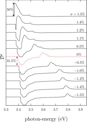
For Si we show in Fig. 1 the calculated vs. the photon energy for several values of , including both expansive and compressive strains, along with the result of the unstressed () result. We vary from to 1.5%. The unstressed spectrum shows two main features, one at 3.425 eV, just a few meV above the band gap with a deep, and the other at 3.593 eV with a peak. As we compress the unit cell () we see that the negative deep remains almost unchanged in magnitude and energy position, however the positive peak moves towards higher energies, keeping almost the same shape and showing a modest reduction to 11% at . This situation changes radically when we expand the unit cell. Indeed, as increases the negative deep gets narrower, slightly moves to lower energies and then disappears at . The positive peak in turn moves to lower energies, increases its height and its shape changes until it gives a that rises sharply at the band edge with a maximum intensity of 50%. The spectrum at only shows this positive peak that has the largest magnitude of all the spectra. Thus, under expansive stress bulk Si exhibits a quite interesting response: the negative deep and positive peak shown in for the unstressed unit cell coalesce into a single positive peak at the band edge with of the spins polarized along the direction of propagation of the optical beam. We have checked that for , the only shifts the spectrum to lower energies, retaining the magnitude of the DSP signal peak at . Nevertheless such large expansions may be experimentally more difficult to achieve.not
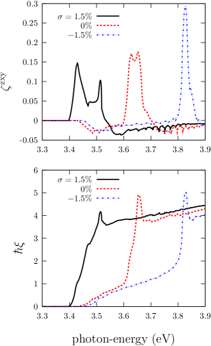
In Fig. 2 we show the calculated and for . We remark that in Gaussian units both tensors are dimensionless quantities. We see that the onset at the band-edge is red-shifted in energy as goes from to 1.5%. For both and is negative around the onset, whereas it is positive for and rises very sharply. For we see that the rise of the signal at the onset changes also with , being rather sharp for as it is for . From these results, one can understand the line shape of shown in Fig. 1. Indeed, the minimum (maximum) present in for , comes from the minimum (maximum) in , whereas the only one maximum of for near the band-edge comes from the maximum at , but then the next local maximum in is barely seen in since, as shown in the Fig. 2, the corresponding is rather large as compared with . In other words, the DSP depends strongly on the fine interplay between the ability for polarizing the spin of the electrons, and the number of electrons (carriers) that one can inject.
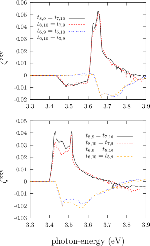
The rate of spin injection from the different transitions in our calculation can be seen more clearly in Fig. 3, where we show for selected transitions from the valence bands () to the conduction bands (), for and . We only show the transitions that have the most influential effect on the net spin-injection rate. We label the bands in ascending values of energy, thus is the top valence band and is the bottom conduction band. We use to denote a transition from () to (). Indeed, we see how the onset of the response is mainly given by the contributions of , , , , , , , and , where the following relationships, traceable to the symmetry of the states,Nastos et al. (2007) are found: , , , and . These are the transitions from the last four valence bands to the bottom of the first two conduction bands. We see that the onset of the signal at the corresponding band edge for each value of is due to the and the transitions. These transitions for have a that is first negative from 3.40 eV till 3.58 eV, and then becomes positive and goes to almost zero above 3.86 eV. However, for the same transitions at , the corresponding is always positive and goes to almost zero above 3.9 eV. Also, the spectra shows that the and the transitions kick in above the band gap and that for both values of the corresponding is always negative. But now we note that, for , these transitions kick in 200 meV above the band gap, whereas for the signal kick in just 32 meV above the band gap. This large difference in turn gives the observed in Fig. 1, i.e. for we have a broad minimum at 25 meV above the band edge, followed by a broad maximum at 195 meV above the band edge, whereas for we have a sudden build up of at the band edge followed by a rapid decrease of the signal to zero.
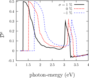
Finally, in Fig. 4 we show for GaAs the calculated vs. the photon energy for three values of , one for expansive stress, one for compressive stress, and the other one for the unstressed () result. The unstressed spectrum shows two positive peaks, one at 1.5 eV, just at the band edge of GaAs with , and the other at 3.18 eV with . As we expand (compress) the unit cell to () we see that the spectrum shifts almost rigidly along the energy axis towards lower (higher) energies, with only a very small change in the intensity of the peak at 3.1 eV. This behavior remains valid for larger values of . For the unstressed case of GaAs, the value of the has been confirmed experimentally,Bhat et al. (2005) and explained theoretically,Nastos et al. (2007) thus our calculated results indicate that either compressive or expansive strain will only move the onset of the signal. This also shows that the symmetry of the electronic band structure that leads into the results shown for remains basically the same as we apply the stress,Nastos et al. (2007) in contrast with Si, where the changes of are readily noticeable.
We have presented a study of optical spin injection rates for stressed bulk Si and stressed bulk GaAs. Both compressive and expansive stress can effectively modulate the degree of spin polarization in these materials. For bulk Si, compressive stress shifts the positive peak of to higher energies and diminishes the signal about of its value for the unstressed case. On the other hand, the negative deep remains almost unchanged both in energy position and magnitude. Contrary to this behaviour, for expansive stress we found that the DSP signal is notably enhanced. For of volumetric change the line shape of the signal changes from the one negative deep and one positive peak of the unstressed case to two positive peaks. One at the band edge with 50% of DSP and the other with an almost negligible magnitude. Thus, expansive strain changes the DSP from of the unstressed case to . Further expansion shifts this positive peak to lower energies without changing its magnitude. For bulk GaAs, compressive and expansive stress rigidly shift the spectrum to higher or lower energies, respectively, maintaining the band edge peak signal at . The results presented in this work show that the application of stress can be employed to tune the material to a suitable photon energy and, more importantly, to increase net DSP for the case of Si, making this material just as efficient as GaAs. We believe this ought to motivate the experimental verification of the theoretical results presented here.
We acknowledge useful discussions with F. Nastos, J. Sipe and S. Turneaure. BSM acknowledges partial support by CONACYT grant 48915-F, and CS and JLC scholarships by CONACYT and CONCYTEG.
References
- Zutic et al. (2004) I. Zutic, J. Fabian, and S. D. Sarma, Reviews of Modern Physics 76, 323 (2004).
- Dyakonov and Perel (1984) M. I. Dyakonov and V. I. Perel, Optical Orientation (Edited by F. Meier and B. P. Zakharchenya (Elsevier, Amsterdam) chap. 2, pp. 11-71, 1984).
- Lampel (1968) G. Lampel, Phys. Rev. Lett. 20, 491 (1968).
- Nastos et al. (2007) F. Nastos, J. Rioux, M. Strimas-Mackey, B. S. Mendoza, and J. E. Sipe, Phys. Rev. B 76, 205113 (2007).
- Cabellos et al. (2009a) J. Cabellos, B. Mendoza, F. Nastos, T. Rangel, N. Arzate, and J. Sipe, Phys. Rev. B p. submitted (2009a).
- (6) Stefan Turneaure, private communication.
- Hilton and Tang (2002) D. J. Hilton and C. L. Tang, Phys. Rev. Lett. 89, 146601 (2002).
- X.Gonze et al. (2002) X.Gonze, J.-M. Beuken, R. Caracas, F. Detraux, M. Fuchs, G.-M. Rignanese, L. Sindic, M. Verstraete, G. Zerah, F. Jollet, et al., Computational Materials Science 25 (2002).
- Hartwigsen et al. (1998) C. Hartwigsen, S. Goedecker, and J. Hutter, Phys. Rev. B 58, 3641 (1998).
- Goedecker et al. (1996) S. Goedecker, M. Teter, and J. Hutter, Phys. Rev. B 54, 1703 (1996).
- Mendoza et al. (2006) B. S. Mendoza, F. Nastos, N. Arzate, and J. E. Sipe, Physical Review B 74, 075318 (2006).
- Read and Needs (1991) A. J. Read and R. J. Needs, Phys. Rev. B 44, 13071 (1991).
- Kageshima and Shiraishi (1997) H. Kageshima and K. Shiraishi, Phys. Rev. B 56, 14985 (1997).
- Cabellos et al. (2009b) J. Cabellos, M. Escobar, B. Mendoza, F. Nastos, and J. Sipe, Phys. Rev. B p. submitted (2009b).
- Nastos et al. (2005) F. Nastos, B. Olejnik, K. Schwarz, and J. E. Sipe, Physical Review B 72, 045223 (pages 9) (2005).
- (16) Essentially, for a 0 to volumetric expansion, the signal peak shifts from 3.5 eV to 1.5 eV, thus sweeping a large portion of the optical range.
- Bhat et al. (2005) R. D. R. Bhat, P. Nemec, Y. Kerachian, H. M. van Driel, J. E. Sipe, and A. L. Smirl, Physical Review B 71, 035209 (2005).