Characterization of Hamamatsu 64-channel TSV SiPMs
Abstract
Aims.
The Hamamatsu UV-light enhanced 64-channel SiPM array of the newest generation (S13361-3050AS-08)
has been examined for the purpose of being used for the Silicon Elementary Cell Add-on (SiECA)
of the EUSO-SPB balloon experiment.
At a room temperature of , the average measured breakdown voltage of the array is
V, the average gain is measured to and the
average photon detection efficiency
results to at a wavelength of and a bias voltage of V.
The average dark-count rate is MHz,
equivalent to a dark-count rate per SiPM area of ,
and the crosstalk probability is measured to .
These results confirm the information given by the manufacturer.
Measurements performed with the newly installed Single Photon Calibration Stand at KIT (SPOCK)
show the improved sensitivity to photons with wavelengths lower than nm
compared to the SiPM array S12642-0808PA-50, which was also investigated for comparison.
Additional measurements confirm the strong temperature dependence of
the SiPM characteristics as given in the data sheet.
All the characterized parameters appear to be sufficiently uniform to
build up a focal surface of SiPM arrays fulfilling the requirements
for a telescope detecting photons in the UV range.
Methods.
Results.
doi:
10.1088/1748-0221/4/04/P04004doi:
10.1016/j.nima.2010.03.169doi:
http://dx.doi.org/10.1016/j.asr.2013.11.056doi:
https://doi.org/10.1016/j.astropartphys.2013.01.008doi:
https://doi.org/10.1016/j.nima.2016.09.053doi:
10.1088/1748-0221/3/10/P100011 Introduction
Silicon Photomultipliers (SiPMs) are a new type of photo detectors Renker and Lorenz (2009)
capable of
detecting single photons with photon detection efficiencies in reasonable operation
of up to 40% and single photon time resolutions of several hundred picoseconds Nemallapudi et al. (2016).
Due to the great progress of SiPM development during the recent years, SiPMs
are in many ways comparable to conventional Photo Multiplier Tubes (PMTs) which have ruled the
field of photon detection for decades.
SiPMs have several advantages including a much lower operation voltage, a
lightweight and robust structure and an insensitivity to magnetic fields Eckert et al. (2010).
SiPMs are robust against too much incident light: Instead of burning the collecting
anode of a PMT, a SiPM enters saturation and draws constant current but it is not damaged.
However, SiPM properties are highly temperature dependent. The dark-count rate of SiPMs at room
temperature is in the MHz regime which is much higher than the kHz dark-count rate of conventional
PMTs.
The present task of characterizing SiPM arrays is embedded in the Extreme Universe Space Observatory
(EUSO) project. EUSO aims to detect Extensive Air Showers (EAS) induced in
Earth’s atmosphere by ultra-high energy cosmic rays. Instead of detecting EAS by looking from the
Earth up into the atmosphere, EUSO aims to detect EAS by looking from space down into the
Earth’s atmosphere Ebisuzaki et al. (2014). EAS can be detected by measuring fluorescence light
emitted by nitrogen molecules excited during
an EAS. Nitrogen emits fluorescence photons mostly in the UV range between nm.
The expected flux of fluorescence photons during an EAS measured from a
height of around km above ground, which resembles the flight height of the International
Space Station (ISS), is around 400 photons per s and square meter for a eV EAS J.H. Adams et al. (2013).
Looking at these limits, a good photon detection efficiency in the UV range and the
ability of measuring single photons are constraints for the photon detection device used in EUSO.
In the standard design, the focal surface of the EUSO telescope
consists of 64-channel Multi-Anode PMTs (MAPMTs).
A technological evaluation of the EUSO detection system with a scaled down telescope was flown as
the payload of the NASA 2017 Super Pressure Balloon (SPB) mission with the expected duration of at
least 60 days at an altitude of km. In parallel with the main camera ( MAPMTs arranged in nine elementary cells), the Silicon Elementary Cell
Add-on (SiECA) camera was mounted in the optical focal plane. It was centered on one edge of the MAPMT
camera such that a cosmic ray event could pass through the field of view of both
cameras Wiencke (2017). This opportunity to evaluate MAPMT and SiPM detection systems under
identical conditions has provided extensive experience and data for ongoing evaluation of the two
methods of low photon intensity signal detection. Due to the 12-days flight time that was realized
on this experimental delivery system, additional tests are in preparation to evaluate the SiECA
camera while analysis of the SPB flight data regarding possible EAS event(s) and UV background
measurement is ongoing Painter (2017).
Characterization results for the two 64 channel Hamamatsu SiPM arrays S12642-0808PA-50
(S12) and S13361-3050AS-08 (S13) are presented.
The S12 SiPM array was released in 2014.
The next series SiPM array S13 was released in 2015.
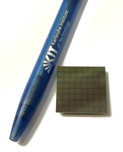
Both SiPM arrays consist of 64 Through-Silicon-Via (TSV) SiPM channels with 3584 Avalanche
Photo Diodes (APDs) in each channel and a pitch distance of m between the APDs.
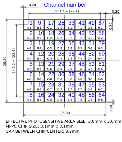
Figure 1 shows the ordering of the 64 channels and the size of the
arrays which are the same for both arrays S12 and S13 (figure 1).
Through-Silicon-Via means that the cathode is etched through the silicon waver in the middle of
the SiPM, building an electrical interconnection from the surface to the bottom of the SiPM device.
Since the channel wires are attached on the back side of the SiPM array, the space between two
channels can be reduced from about 3 mm without TSV to about mm.
Both arrays are equipped with Samtec ST4111Samtec ST4-40-1.00-L-D-P-TR
connectors on the backside.
An important difference between the two SiPM arrays is the coating of the SiPM array surface.
The surface of the SiPM array S12 has an epoxy resin. The SiPM array S13
is coated with a silicone resin. The different resins result in a different sensitivity of
UV photons with wavelengths less than nm. With an epoxy resin, the sensitivity for light
in the UV region goes down to a wavelength of nm. With a silicone resin, light with a
wavelength down to nm can be detected. For more information about these specific SiPMs
see Hamamatsu Corporation (2015, 2014a).
2 Measurement setup: The Single Photon Calibration Stand at KIT
The measurements were performed with the Single Photon Calibration Stand at KIT (SPOCK). SPOCK consists of photon shielding, a reference light source, read-out electronics and measurement-controlling software. The photon shielding is a light-tight wooden box covered inside with black flock paper. The reference light source is placed inside of the photon shielding and consists of an integrating sphere, several LED arrays, a NIST-calibrated photo diode and a collimator. The integrating sphere is a Labsphere 3P-GPS-053-SL with a diameter of cm. Four LED arrays, each equipped with several LEDs of the same type and wavelength, are available. These can be attached to the entrance port of the integrating sphere.
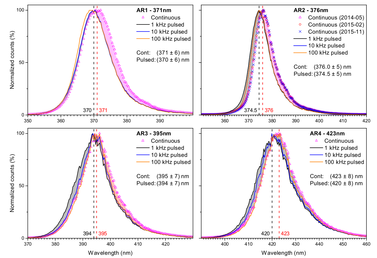
A single LED in the middle of the array can be used in pulsed mode (see table 1). Measurements of the emitted wavelength of the LEDs were performed with an Ocean Optics S2000 spectrometer and the corresponding analogue-to-digital converter Ocean Optics ADC1000-USB in pulsed and continuous mode (see (Karus, 2016)). The results are shown in figure 2. The characterization measurements presented here have been made with the LED array with wavelength nm.
| LED-array | LED | Number of LEDs | Wavelength (nm) |
|---|---|---|---|
| Array 1 | UVLED365-110E | 42+1 | |
| Array 2 | XSL-375-3E | 20+1 | |
| Array 3 | VL390-5-15 | 42+1 | |
| Array 4 | VL425-5-15 | 12+1 |
The NIST-calibrated photo diode measures the optical power inside of the integrating sphere. A collimator can be screwed to the exit port of the integrating sphere to reduce the optical power leaving the integrating sphere by a factor of . Together with the monitoring of the optical power inside of the integrating sphere, this allows emitted light with a known optical power onto the SiPM down to one photon per pulse in average. During the characterization measurements the optical power inside the sphere moved in the range of pW, resembling an output of two to four photons per pulse after the collimator.
The optical power during the measurement of each SiPM channel is monitored and stored. The overall change of the optical power results from variations in the output power of the light diode driver during the whole measurement time.
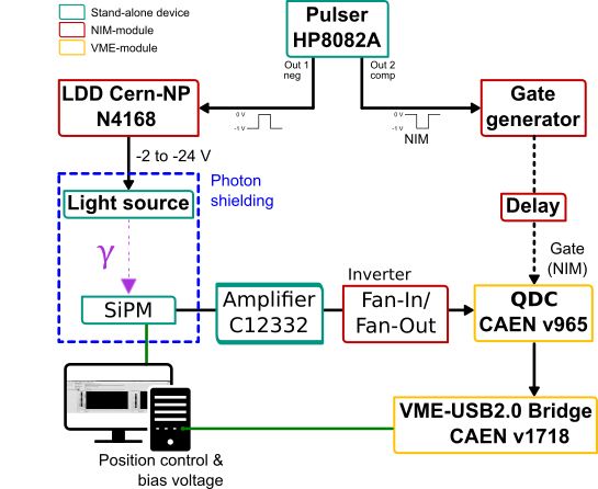
A pulse generator HP8082A generates simultaneously two pulses which are guided to a Light Diode Driver (LDD) and a gate generator (see figure 3). The LDD generates a variable pulse to drive the pulsed LED in the LED array. The gate generator generates the gate during which the Charge-to-Digital Converter (QDC) integrates the incoming SiPM signal.
The SiPM is placed on a read-out board a few millimetres in front of the collimator exit. The board is a customized two-layer PCB222Printed Circuit Board which guides the cathode signal of each SiPM channel to a pin connection. A channel is selected by closing the pin connection of the particular channel, i.e. only one channel can be read out at a time.
The SiPM signal is passed via a coaxial cable to the amplifier circuit of a SiPM Evaluation Board C12332 manufactured by Hamamatsu. The C12332-Board has been modified for the purpose of amplifying incoming lemo signals. The on-board amplifier IC Texas Instruments OPA864 amplifies the SiPM signal by a factor of . Figure 4 shows the measurement setup inside SPOCK.
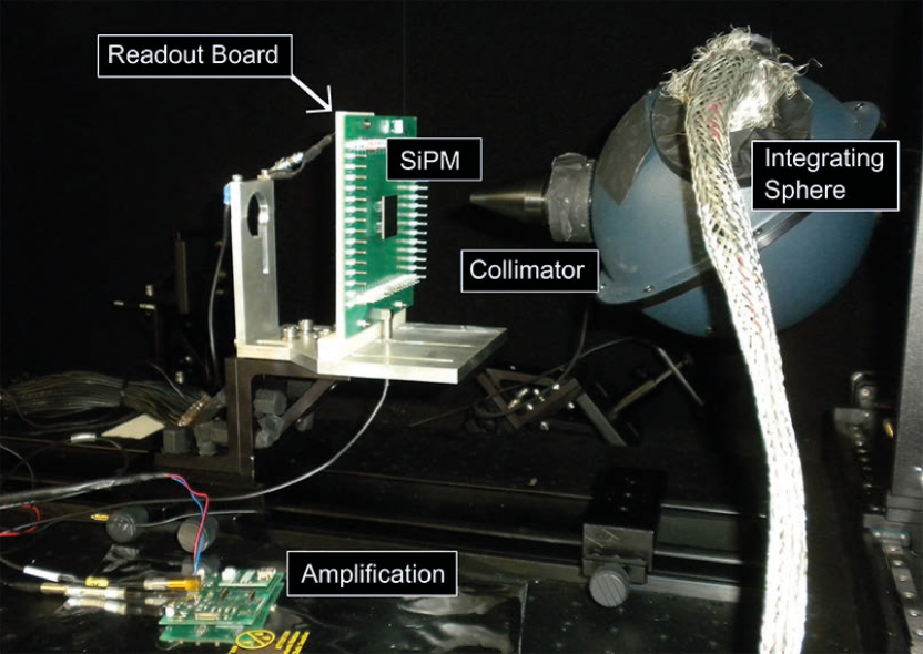
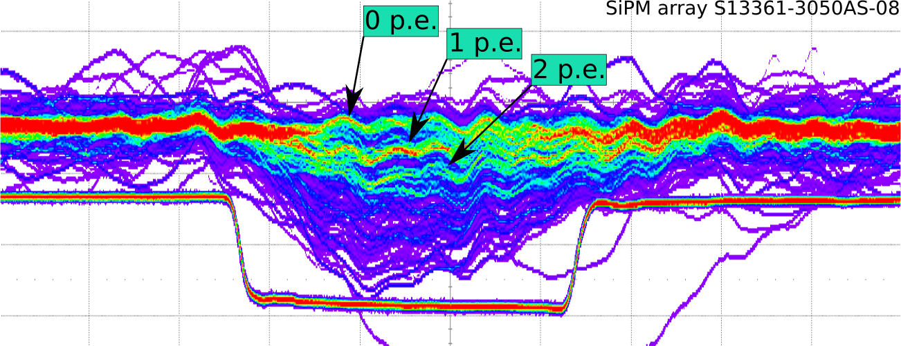
The amplified SiPM signal is passed to a Fan-in/Fan-out which inverts the SiPM signal before it is guided into a QDC CAEN v965. The QDC integrates the signal’s charge during a variable gate time. The integration starts ns after the gate signal has been received by the QDC and ends with the end of the gate signal. For the present measurements, the gate length was chosen to be ns including the ns activation time of the QDC. This gate length covers most of the SiPM signal and avoids probable after-pulses which should not be recorded (Fig. 5). The gate is set with the help of delays between gate generator and QDC in a way that the QDC starts integrating the SiPM signal when signals induced by the pulsed LED are expected. The digitized integrated charge of the signal is recorded with the measurement software written in Labview.
The temperature is monitored during all measurements with a temperature sensor DS18B20 placed inside the shielding close to the SiPM. The measurement environment was cooled by an air condition.
The temperature during the measurements was C.
Temperature dependent measurements have been made to investigate the temperature dependency
of the SiPM characteristics. For this, the SiPM was put into a m2 styrofoam cooling box together with thermal reservoirs, i.e. water packs. The cooling box with the thermal reservoirs and the SiPM was cooled down in a fridge to C and measurements were made inside SPOCK as the system returned to ambient temperature.
3 Measurement methods
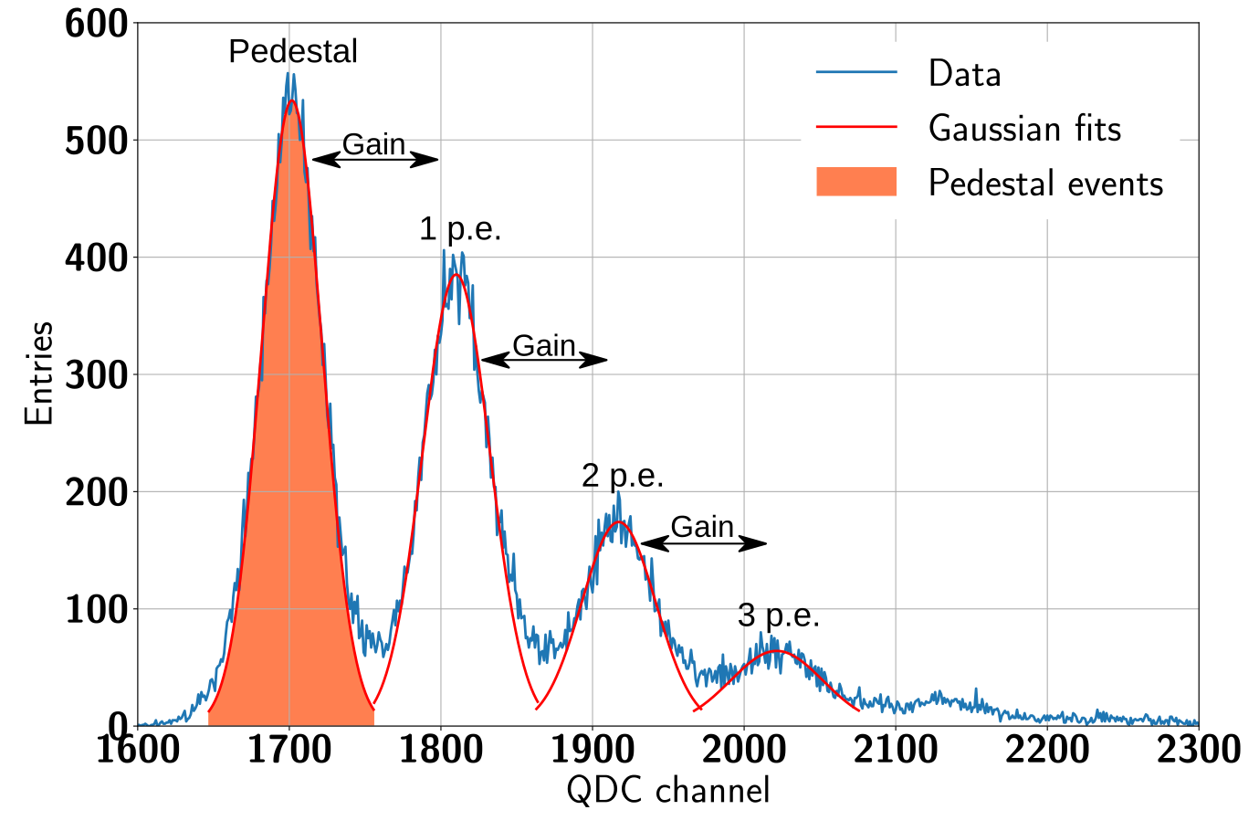
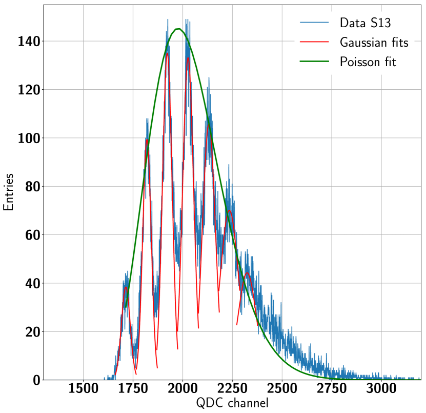
The measurement of the breakdown voltage, the gain, the photon detection efficiency (PDE), the dark-count rate and the crosstalk probability for each channel is made by recording a charge spectrum of the SiPM signals measured with the QDC. An example of a charge spectrum containing 70.000 QDC values is shown in figure 6. The pedestal peak consists of all the events in which no SiPM signal was recorded during a light pulse from the LED. The first photo electron (p.e.) peak contains all the events in which one APD fired and so on. Gaussian fits of the form
| (1) |
with in units of QDC channel, the peak position , the area under the Gaussian function and the standard deviation are performed to every individual peak in the charge spectrum.
The gain of a SiPM channel can be derived easily from the charge spectrum by measuring the distance between consecutive p.e. peaks. The Gain is measured in units of QDC channels. The real Gain can be calculated as
| (2) |
with the QDC channel-to-charge transforming factor , which is known from the calibration of the QDC Karus (2016), the SiPM signal amplification factor and the elementary charge . The amplification factor has been measured by amplifying rectangular pulses of known height with variable widths up to some hundreds of nanoseconds.
The statistical and systematic uncertainties on the gain come from the statistical and systematic uncertainties on the measured distance between consecutive p.e. peaks and the channel-to-charge transforming factor . The uncertainty of the amplification factor contributes only to the systematic uncertainty.
Photon detection efficiency
The PDE can be calculated as
| (3) |
where is the number of measured photoelectrons which equals the number of detected photons and is the number of incident photons per pulse. The number of incident photons is
| (4) |
where is the total optical power inside of the integrating sphere, is the collimator ratio, is the geometrical fill factor which is the fraction of the incident light hitting the SiPM active area, the photon energy of one photon and the light-pulse frequency. Since the collimator was placed right in front of the selected SiPM channel, the geometrical fill factor is assumed to be . For the number of the measured photoelectrons one can make use of Poisson statistics Eckert et al. (2010): The charge spectrum of an ideal SiPM has the form of a Poisson distribution
| (5) |
with the average number of detected photons per pulse as mean value and as the number of measured photoelectrons which equals the pedestal peak (, no photoelectron measured) and the p.e. peaks () for an ideal SiPM. Due to crosstalk, afterpulsing and dark counts, the Poisson behavior of peaks after the pedestal is modulated. The pedestal itself is not influenced by crosstalk and afterpulsing and can be corrected for dark count events by calculating the dark count ratio with the help of a dark spectrum, i.e. a charge spectrum without incident light. So, the mean number of measured photoelectrons can be derived by
| (6) |
where and are the pedestal events (see figure 6) in the measured charge spectrum and the dark spectrum (see figure 7). and are the total numbers of events in the charge spectrum and the dark spectrum.
The uncertainties of the PDE consist of the statistical and systematic uncertainties of the number of incident photons and the number of detected photons .
The statistical uncertainty of comes from the measurement of the light power inside the integrating sphere and the measurement of the collimator ratio. Regarding the systematic uncertainty, also the uncertainties of the LED wavelength and the pulse frequency come into play.
The statistical uncertainty of stems from the uncertainty of the number of pedestal events coming from the Gaussian fits to the pedestal peaks.
The systematic uncertainty of comes from the systematic uncertainty in the number of pedestal events. This uncertainty is with the number of measured pedestal events and has its origin in the QDC non-linearity Karus (2016).
The average relative statistical and systematic uncertainties of and are of more or less equal size in the region of 1% (statistical uncertainty of and ) to about 3.4% (systematic uncertainty of ).
Breakdown Voltage
The breakdown voltage of a SiPM channel is determined by measuring the gain of the SiPM at different bias voltages above the assumed breakdown voltage. A linear regression is made regarding the gain-bias voltage behavior of the SiPM. The linear regression is extrapolated to the voltage value for which the gain of the SiPM becomes zero. This voltage is defined as the breakdown voltage of the SiPM channel. The gain was measured for 15 different bias voltages decreasing in voltage steps of V. The linear regression of the gain-voltage dependence takes the statistical and systematic uncertainties of the gain measurement into account. The resulting uncertainty in the breakdown voltage comes from the uncertainties in the fit results and represents the sum of the statistical and systematic uncertainty.
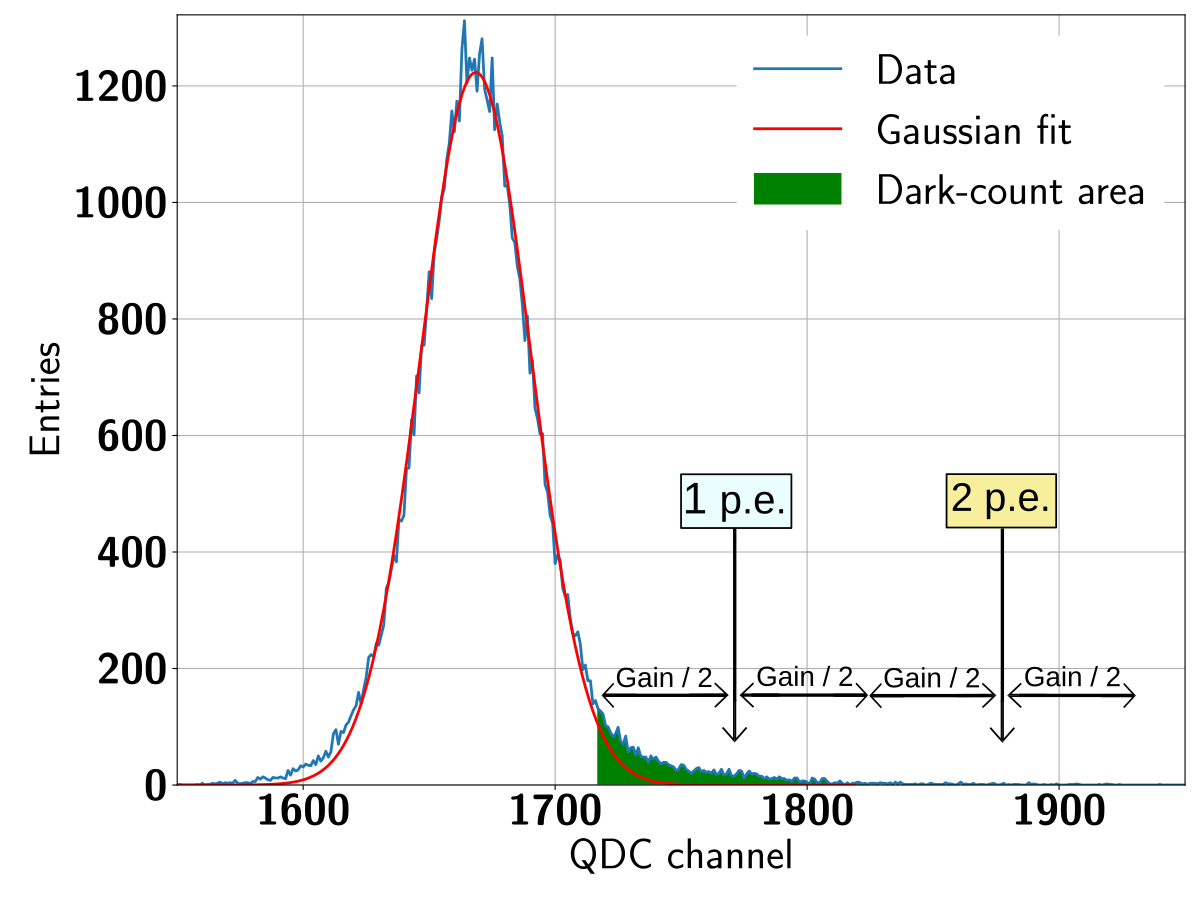
Dark-count rate
To measure the dark-count rate, a dark spectrum of the SiPM is recorded with no light incident on the SiPM. This dark spectrum mainly consists of the pedestal peak (see figure 7). Dark counts generate entries in the first p.e. peak. Due to possible crosstalk events induced by dark counts, also entries located in the second and maybe higher p.e. peaks have to be included. Although the p.e. peaks are not visible in the dark spectrum, the positions of the peaks can be found since all peaks are located at multiples of the gain with respect to the pedestal peak position. The peak area is assumed to be around the p.e. peak position. To calculate the dark-count rate, the events in the area of the first and second p.e. peak are summed and divided by the total measurement time of the QDC. Dark count events higher than the second p.e. peak level are highly unlikely. To reduce the influence of noise to the measurement results, events located in higher p.e. peaks than the second p.e. peak are neglected.
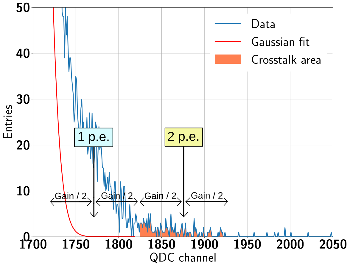
Crosstalk probability
The crosstalk probability is determined with the same SiPM dark spectrum which is used for analyzing the dark-count rate. All pure dark count events are located around the first p.e. peak. If a dark count event induces a crosstalk photon which fires an adjacent APD, this will generate a second p.e. event. So all second p.e. events are considered as cross talk events (see figure 7). Crosstalk events shared between adjacent SiPM channels can not be investigated with the actual measurement setup, but multi-channel crosstalk events are much less likely than single-channel crosstalk events due to the gap between adjacent channels.
The crosstalk probability is calculated by the fraction of the number of crosstalk events and the number of dark count events already determined. The statistical and systematic uncertainties of the number of dark count and crosstalk events are responsible for the uncertainties of the crosstalk probability.
To determine the breakdown voltage, 15 charge spectra containing 15.000 QDC values each have been recorded. For measurements of the gain, the PDE, the dark-count rate and the crosstalk probability, charge and dark spectra with 70.000 QDC values have been used. Using these parameters, the characterization of one SiPM channel took about 20 minutes.
4 Results
One of the main results is that the SiPM array
S13361-3050AS-08 has not only an improved UV-light sensitivity (see section 4.2),
for which it was built, but also has better performance in most of the other properties measured.
Therefore, the characterization results of the 64 channel SiPM array S13361-3050AS-08
(S13) will be presented in detail. It is the newer product from Hamamatsu and finally
chosen for SiECA.
The characterization of the array S12642-0808PA-50
(S12) from an older series will be briefly mentioned for comparison.
All the characterizing measurements of the SiPM array S13 have been made in a series
at a constant bias voltage of V and at a room temperature of .
The incident pulsed light had a wavelength of nm, a pulse frequency of kHz
and a pulse width of ns. Unfortunately, the SiPM channels D1 (channel number 25, see fig. 1),
G5 (channel number 53) and H2 (channel number 58) could not be read out due to a wear out
of the Samtec connectors on the read-out board. These channels are not used for the analysis.
The results are given as the mean value of the results of all measured channels together with its standard deviation.
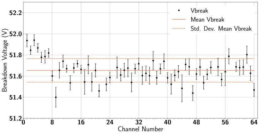
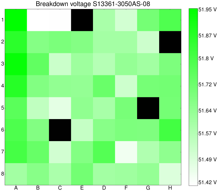
Breakdown voltage
Figure 8 shows the result of the breakdown voltage measurement of the available SiPM channels. Unfortunately, the breakdown voltage measurement failed for channel C6 (channel number 22, see fig. 1). Reasons for this might be a sudden electric noise pollution which was observed several times during the measurements or a temporary malfunction of the Samtec connectors. The mean breakdown voltage over the measured channels of the array is
| (7) |
at a mean measurement temperature of C. This value is consistent with the manufacturer’s information of V at C. All breakdown voltage values are placed in a voltage band with a width of V. Regarding a uniform operation for all SiPM channels in the array, these small inhomogeneities can easily be handled by modern ASICs for SiPM read-out if one power supply for each channel is not an option. In this case, a few power supplies generate the overvoltage and the ASIC fixes the slight differences between the channels due to the different breakdown voltages. This method is applied in SiECA where the ASIC Citiroc manufactured by Weeroc is used for this task Weeroc (9999).
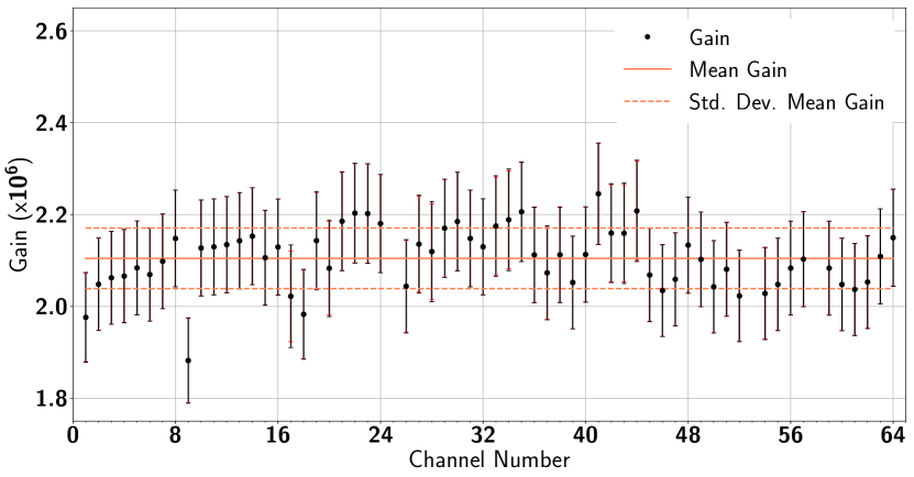
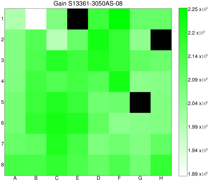
Gain
The results of the gain measurement of array S13 are shown in figure 9. The gain describes the amplification of the first photo electron generated by an incident photon. The mean gain over the whole array is
| (8) |
The data sheet of S13 reports a gain of at a temperature of C, an overvoltage of V and at a wavelength of nm. Since the measurements presented here have been made at a higher overvoltage of V, a slightly higher gain is expected. The inhomogeneity in the gain over the whole array can mostly be explained by the inhomogeneity of the breakdown voltage of the different channels of the array (see also fig. 13). Since the characterization measurements were made with a constant bias voltage of V, a lower breakdown voltage of a SiPM channel leads to a higher overvoltage during the characterization measurement with respect to the mean value. Since the gain depends strongly on the overvoltage of the SiPM, the measured gain of this channel will be higher than the mean gain value.
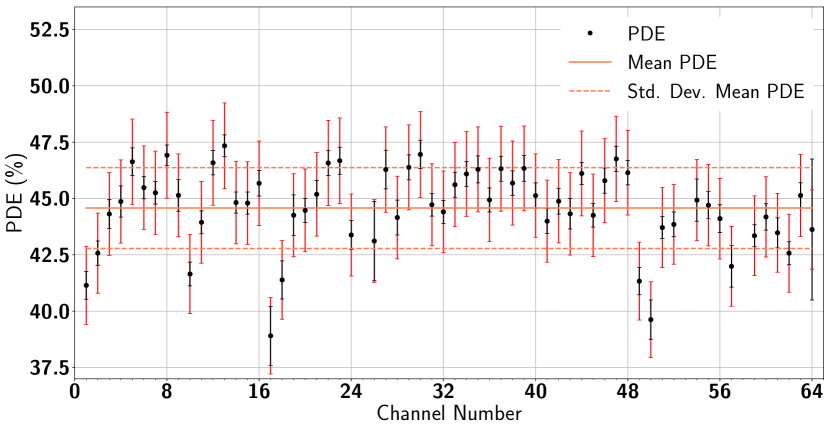
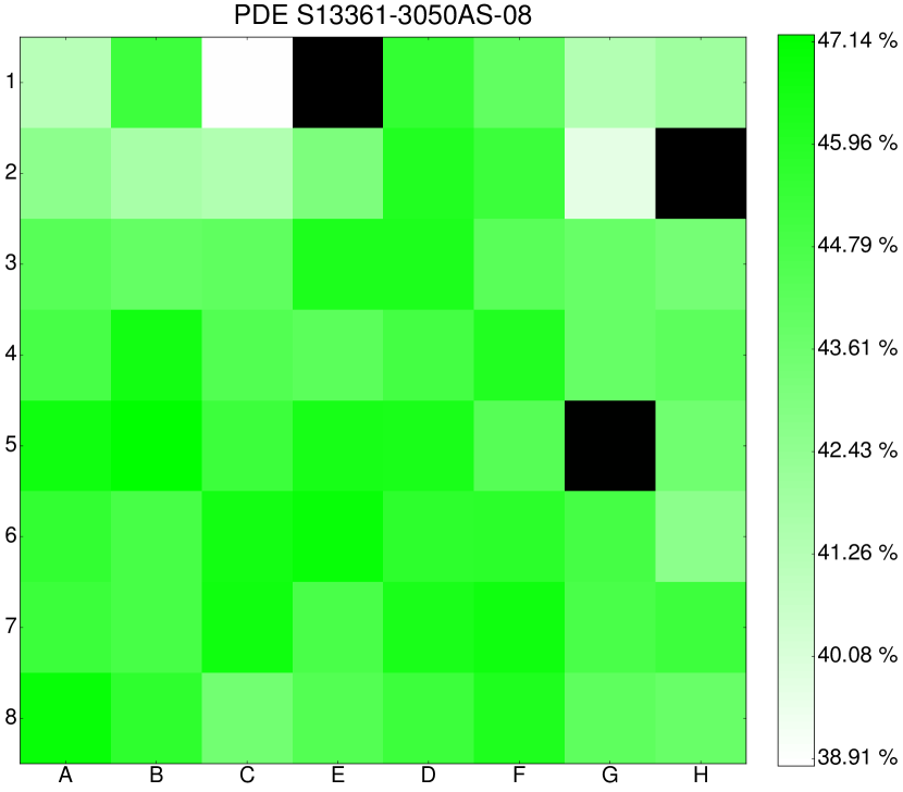
PDE
In figure 10 the results of the PDE measurement are shown. The mean PDE over the whole array is
| (9) |
at a temperature of C and an overvoltage of V. This is about higher than the manufacturers prediction of which again can most probably be explained with the higher overvoltage used in the characterisation measurements. The measured result is comparable to a measurement of a one channel SiPM Hamamatsu S13360-3050CS in Otte et al. (2017).
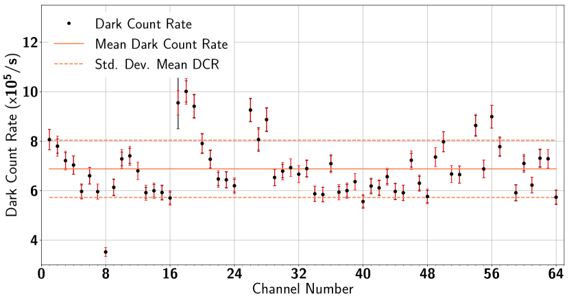
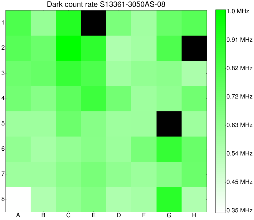
Dark-count rate
The dark-count rate results are presented in figure 11. The mean dark-count rate per channel is
| (10) |
This is comparable to the dark-count rate given in the data sheet with to MHz at C and with an applied overvoltage of V. Nevertheless, the measured variation in the dark-count rate of circa between the different channels of the array is apparently large. A reason for this might be the variation in the breakdown voltages between the channels. Also, since the dark-count rate is a highly temperature dependent characteristic (see figure 20), the temperature change in the range of C during the measurement of different channels is expected to have a visible influence on the dark-count rate results (see section 4.3 for more information).
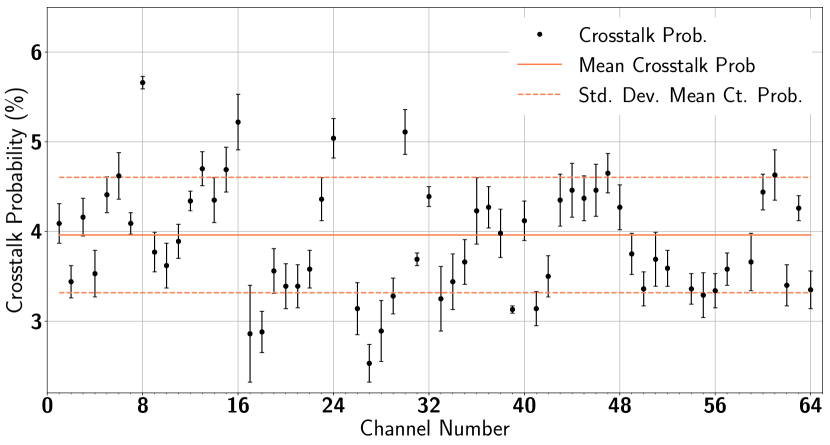
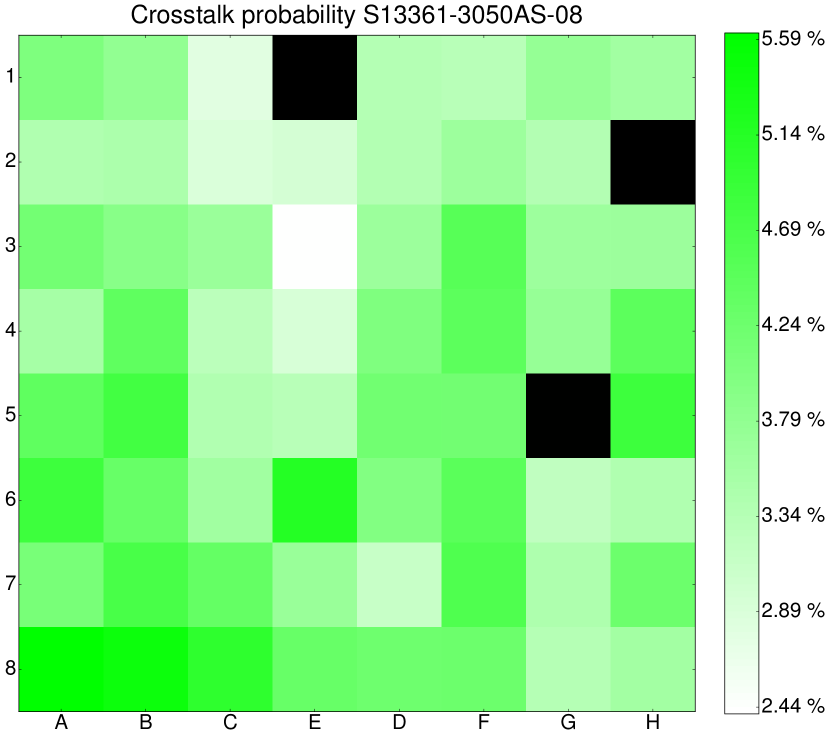
Crosstalk probability
The crosstalk probability is shown in figure 12. The mean crosstalk probability is
| (11) |
This value is less than half of the value of former SiPM generations for which crosstalk probabilities of more than are typical. The manufacturer claims a probability of at an overvoltage of V. The distribution of the measured values over the array can be seen in figure 13. Since the crosstalk probability depends on the number of adjacent APD cells, a lower crosstalk probability for channels at the edge of the array might be reasonable. Nevertheless, a lower crosstalk probability for channels at the edge of the array is not visible. A logical reason for this is the gap between the channels in the array of about mm. Since this gap surrounds every channel and suppresses the exchange of crosstalk photons between different channels, the location of a channel in the array has no influence on the crosstalk probability.
The characterizing measurements of array S12642-0808PA-50 were made at a bias
voltage of V with the same light source. Table 2
shows the measurement results of array S12 and S13 together with a comparison.
The new series SiPM array S13 has improvements in all of the measured characteristics.
In addition to the channels D1 (channel number 25, see fig. 1) , G5 (channel number 53) and H2 (channel number 58)
which already could not be read out during the measurement of SiPM array S13,
the channels G4 (channel number 52) and G2 (channel number 50) could not be read out in this
consecutive measurement of SiPM array 12642 due to a wear out of the Samtec connectors
on the read-out board.
Information about the uniformity of the measured characteristics of S13 are visualized in
figure 13. An overall uniformity of the single channels of the array is given and
sufficient for building a homogeneous SiPM focal surface. Differences, especially in the single
channel breakdown voltages, are small enough to be fixed by ASICs.
Nevertheless, the variations in, for example, the PDE or the dark-count rate seem quite large.
By adjusting the bias voltage individually for every single channel of the array so that
every channel works with the same overvoltage, the overall uniformity should increase
significantly, which is subject of further studies using the next version of SiECA.
For SiECA, the individual bias voltage adjustment has successfully been realized with the Citiroc ASIC
to guarantee a homogeneous focal surface.
| S12642 | S13361 | Comparison | |
|---|---|---|---|
| Breakdown voltage (V) | -20 % | ||
| Gain () | +28 % | ||
| PDE ( % ) | +25 % | ||
| Dark-count rate (MHz) | -43 % | ||
| Crosstalk probability (%) | -65 % |
4.1 Response behaviour
In addition to the characterization measurements, the response behavior of the two SiPM arrays
has been investigated.
Due to the working principle of a SiPM, the signal is not always proportional to the number of
incident photons. The reason for this is that the signal of the single Avalanche Photo Diode (APD)
is not sensitive to the number of photons hitting the APD, but digitally fires or not.
For large numbers of incident photons, the total SiPM signal saturates with available APDs activated.
The SiPM response behaviour describes the SiPM signal regarding a variable number of incident photons.
This is the number of firing APDs
with respect to the number of incident photons (see eq. 4).
For the response behaviour measurement, the same light source as for the characterization measurements
with photons of a wavelength of nm was used.
The number of firing APDs was determined by fitting a Poisson-like distribution of the form
| (12) |
to each measured charge spectrum. Here, is the mean number of fired APDs and is the p.e. peak index (see equ. 5). To obtain reasonable fit results, the factor was included in the fit function to take care of the height of the charge spectrum. As data points for the Poisson fit, the maxima of the Gaussian fits of the single p.e. peaks have been chosen. To transform the position of the Gaussian maxima from QDC channel to p.e. peak index , the position was divided by the gain measured with the actual charge spectrum. The overall spectrum was subtracted by the pedestal peak position to start with a value of for the pedestal peak. If a gain measurement failed since the incoming light had a too low intensity to create a sufficient charge spectrum, the gain value measured during the characterization of the actual channel was chosen and the fit data points have been selected as the charge spectrum entries at the position of multiples of this gain.
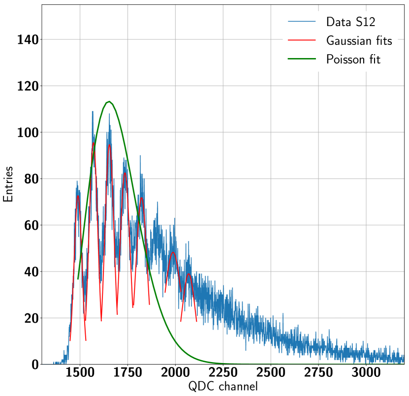
Examples of the Poisson fit for two charge spectra of array S12 and S13 are shown in figure 14. Both measurements have been performed with a comparable number of incident photons (S12: 6.77 photons/pulse, S13: 6.83 photons/pulse). For array S13, the Poisson fit resembles the form of the charge spectrum and gives a good estimate for the mean number of fired APDs. Regarding array S12, the fit can be performed but is disturbed by the long tail of the charge spectrum coming from afterpulses, crosstalk and dark counts. Due to this, the fit result for the mean number of fired APDs is shifted towards higher values for an increasing number of incoming photons.
The number of firing APDs was calculated for several numbers of incident photons in the range of zero and 10 photons per pulse. The measurement has been performed for one channel of each array. For the SiPM array S13, channel A3 (channel number 3) has been used. The measured channel of array S12 was B4 (channel number 12).
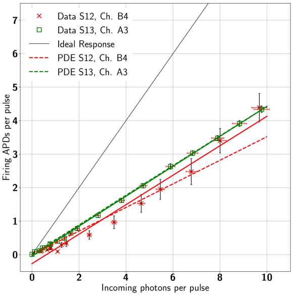
Figure 15 shows the results of the response behaviour measurement. Linear functions are fitted to the slopes of the measured data. The fit results in
| (13) | ||||
| (14) |
The ideal SiPM response, meaning one firing APD per incoming photon is included in figure 15 as a black solid line. The theoretical response behaviour calculated with the measured PDE for each of the two channels is plotted with dotted lines. This response behaviour follows
| (15) | ||||
| (16) |
The response behaviour of both SiPM arrays have lower inclinations than the ideal response line which is expected
since both arrays have less than PDE. For array S13 the linear fit to the measured values and the theoretical behaviour calculated from the PDE measured in the characterization measurement agree. Regarding the results of array S12, the measured values do not follow the predicted behaviour. This has its reason in the Poisson fit of the charge spectrum, which gives too high results for the mean number of firing APDs for an increasing numbers of incident photons (see fig. 15). Other possibilities for getting the mean number of firing APDs are to calculate the mean or the median of the charge spectrum and determine out of this. But due to the long tail of the S12-SiPM charge spectrum these methods lead to an even higher overestimation of .
Looking at the results for array S13, a linear response behaviour of SiPMs for low numbers of incident photons is visible. The result for the PDE obtained from the characterization measurement and the response behaviour are in coincidence.
Due to the low number of incident photons per pulse, the examined region of the SiPM response is far away
from the region in which the SiPM saturates. Measurements of the dynamic range up to saturation
have been performed elsewhere, e.g. in Bretz et al. (2016).
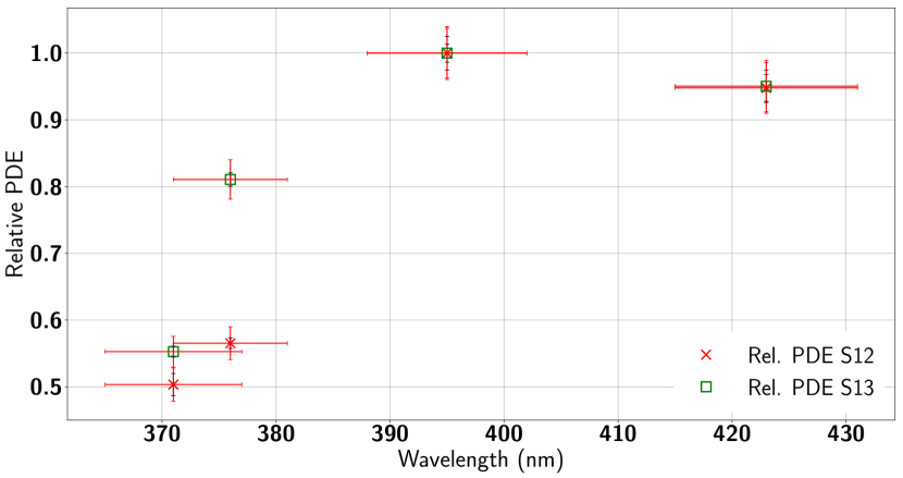
4.2 UV sensitivity
For comparing the UV sensitivity of both arrays, the PDE of one channel of each array was measured at
different wavelengths. The available wavelengths are shown in table 1.
The measurement was done with the B4-channels of both arrays (channel number 12).
Figure 16 shows the results of the measurement.
The relative PDE shown on the y-axis in figure 16 is the measured PDE normalized
to the highest measured PDE value of each channel which was for both channels at a wavelength of nm.
The improvement of SiPM array S13 regarding the sensitivity in UV photons is clearly visible.
For wavelengths lower than nm, the relative PDE of array S13 is apparently higher which
is due to the different resin of the arrays.
Regarding wavelengths below nm, the manufacturer claims sensitivity of the SiPMs to wavelengths
down to nm for the epoxy resin array and nm for the silicone resin array.
4.3 Temperature dependent measurements
Temperature dependent measurements have been performed with channel E4 (channel number 36) of SiPM
array S13361-3050AS-08. The SiPM was put into a cooling box together with thermal reservoirs.
The cooling box with the SiPM placed inside was cooled down in a fridge to about C. The
measurements were performed as the cooling chamber warmed up. For the measurements the cooling
chamber was placed inside of the photon shielding of SPOCK. The temperature rose from C to C and was constantly monitored with a DS18B20 temperature sensor placed near the SiPM.
The bias voltage was kept constant at V.
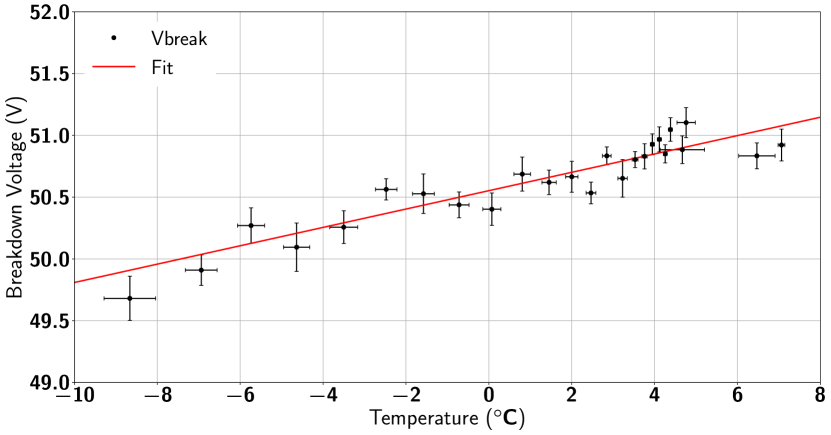
Breakdown voltage
The temperature dependence of the breakdown voltage is shown in figure 17. The breakdown voltage increases linearly with increasing temperature which is the expected behaviour Otte et al. (2017); Hamamatsu Corporation (2014b); Lightfoot et al. (2008). The result for the fit of the breakdown voltage values shown in figure 17 is
| (17) |
The temperature coefficient which gives information about the breakdown voltage behaviour regarding the temperature is measured as
| (18) |
The temperature coefficient provided by Hamamatsu as for the SiPM array S13 is off the measured value.
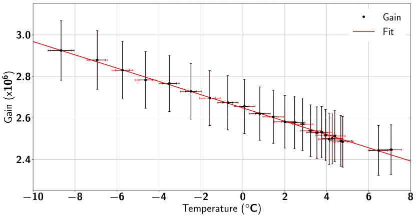
Gain
In figure 18 the measured temperature dependency of the gain is shown. Since the bias voltage was kept constant and the breakdown voltage increased with increasing temperature, the gain is expected to decrease. The measurement confirms this behaviour. The gain decreases by about 10% per 10 degree in the measured temperature range. The fit results are
| (19) |
PDE
A statement about the PDE temperature dependency can not be made.
Since the SiPM was biased with a constant voltage, the PDE should decrease with increasing temperature
due to the increase of the breakdown voltage. The results of the measurements are shown in
figure 19, where it is seen that the PDE values do not follow this expectation.
For temperatures below the freezing point the PDE rises. Above the freezing point, the PDE values seem
to be more or less constant.
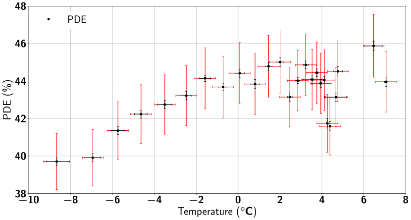
This rather strange behaviour of the PDE could be caused by the formation of an ice or frost layer on
the SiPM’s surface below C preventing photons to penetrate the SiPM.
The SiPM was cooled down inside the cooling chamber together with the thermal reservoirs.
Although the SiPM surface was cleaned from ice before the measurement, a new layer might
have accumulated before the first measurements. With increasing temperature, the ice
layer became thinner which results in a higher PDE. Above the freezing point the ice melted and
water might have covered parts of the SiPM surface leading to the more random like distribution
for temperatures higher than zero degrees. Since the PDE is the only measured SiPM characteristic
that is sensitive to changes in the number of penetrating photons during the measurement,
the other characteristics are not influenced by this circumstance.
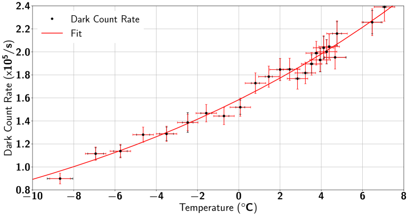
Dark-count rate
Figure 20 shows the dark-count rate measurement results. An increase in dark-count rate with an increase in temperature is clearly visible. Since dark counts are thermally excited electrons, an increase of the dark-count rate with temperature is expected. For a constant gain, the dark-count rate should follow
| (20) |
with the absolute temperature , the band gap energy , the Boltzman constant and an arbitrary constant Hamamatsu Corporation (2014b).
In this measurement, the bias voltage of the SiPM was kept constant and the gain decreased
with increasing temperature (see fig. 18). Therefore, equation 20
is not valid. In the measured region the fit
| (21) |
gives the best results.
5 Conclusion
The characterization-measurement results including breakdown voltage, gain, photon detection efficiency, dark-count rate and crosstalk probability of the two SiPM arrays S12642-0808PA-50 and S13361-3050AS-08 confirm to a large extent the SiPM characteristics given by the manufacturer. The latter SiPM array improved in all of the measured characteristics compared to the older series SiPM array (see table 2 for details). Additional measurements of the response behaviour and of the UV sensitivity show a linear response behaviour for small numbers of incident photons of both arrays and a better UV sensitivity for wavelengths below nm of the array S13361-3050AS-08. Measurements performed with one channel of array S13361-3050AS-08 confirm the strong temperature dependence of the SiPM characteristics.
Due to its better performance, the SiPM array S13361-3050AS-08 has been chosen to be employed in SiECA333Silicon Elementary Cell Add-on. The uniformity of the array is sufficient to build a focal surface out of SiPM arrays. Inhomogeneities between different channels of the SiPM array can be handled by applying individual bias voltages to every channel like it is done in the operation version of SiECA.
The presented newly installed measurement setup at KIT (SPOCK) and the applied methods allow for efficient tests and characterization of SiPMs and SiPM arrays of all kinds and geometries. I.e., the precise characterization of SiPMs can be done for manifold applications and future experiments.
Acknowledgements
We kindly acknowledge the support by the ’Helmholtz Alliance for Astroparticle Physics - HAP’ funded by the Initiative and Networking Fund of the Helmholtz Association. Acknowledgements go also to Hamamatsu Photonics for giving us the opportunity to work with their newest SiPM products. The authors deeply acknowledge all the support by the JEM-EUSO collaboration and in particular by the EUSO-SPB team. The author wants to thank expressly Lawrence Wiencke for his advice during the writing process. An important contribution to the success of this work was made by the technical staff of the IKP at KIT, in particular Heike Bolz and Bernd Hoffmann, as well as by the students Sally-Ann Sandkuhl, Simon Ehnle, Nils Hampe and Sonja Schneidewind.
References
- Renker and Lorenz (2009) D. Renker and E. Lorenz. Advances in solid state photon detectors. JINST, 4:P04004, 2009. .
- Nemallapudi et al. (2016) M.V. Nemallapudi, S. Gundacker, P. Lecoq, and E. Auffray. Single photon time resolution of state of the art SiPMs. Journal of Instrumentation, 11(10):P10016, 2016. URL http://stacks.iop.org/1748-0221/11/i=10/a=P10016.
- Eckert et al. (2010) Patrick Eckert, Hans-Christian Schultz-Coulon, Wei Shen, Rainer Stamen, and Alexander Tadday. Characterisation Studies of Silicon Photomultipliers. Nucl. Instrum. Meth., A620:217–226, 2010. .
- Ebisuzaki et al. (2014) T. Ebisuzaki, Gustavo Medina-Tanco, and Andrea Santangelo. The JEM-EUSO mission. Advances in Space Research, 53(10):1499 – 1505, 2014. ISSN 0273-1177. . URL www.sciencedirect.com/science/article/pii/S027311771300759X.
- J.H. Adams et al. (2013) J.H. Adams et al. An evaluation of the exposure in nadir observation of the JEM-EUSO mission. Astroparticle Physics, 44(Supplement C):76 – 90, 2013. ISSN 0927-6505. . URL http://www.sciencedirect.com/science/article/pii/S0927650513000182.
- Wiencke (2017) Lawrence Wiencke. EUSO-SPB mission and science. PoS, ICRC2017 1097, 2017.
- Painter (2017) William Painter. SiECA: Silicon photomultiplier prototype for flight with EUSO-SPB. PoS, ICRC2017 442, 2017.
- Hamamatsu Corporation (2015) Hamamatsu Corporation. Datasheet 64 channel SiPM array S13361 series, 2015. URL {http://www.hamamatsu.com/jp/en/product/alpha/M/4114/S13361-3050AE-08/index.html}.
- Hamamatsu Corporation (2014a) Hamamatsu Corporation. Datasheet 64 channel SiPM array S12642 series, 2014a.
- Karus (2016) Michael Karus. Development of a calibration stand for photosensors for extremely high-energy cosmic ray research. PhD thesis, Karlsruhe Institut für Technologie (KIT), 2016.
- Weeroc (9999) Weeroc. Weeroc Citiroc datasheet, 9999. URL http://www.weeroc.com/en/products/citiroc-1.
- Otte et al. (2017) Adam Nepomuk Otte, Distefano Garcia, Thanh Nguyen, and Dhruv Purushotham. Characterization of three high efficiency and blue sensitive silicon photomultipliers. Nuclear Instruments and Methods in Physics Research Section A: Accelerators, Spectrometers, Detectors and Associated Equipment, 846(Supplement C):106 – 125, 2017. ISSN 0168-9002. . URL http://www.sciencedirect.com/science/article/pii/S0168900216309901.
- Bretz et al. (2016) T. Bretz, T. Hebbeker, M. Lauscher, L. Middendorf, T. Niggemann, J. Schumacher, M. Stephan, A. Bueno, S. Navas, and A.G. Ruiz. Dynamic range measurement and calibration of SiPMs. Journal of Instrumentation, 11(03):P03009, 2016. URL http://stacks.iop.org/1748-0221/11/i=03/a=P03009.
- Hamamatsu Corporation (2014b) Hamamatsu Corporation. Opto-Semiconductor Handbook, Chapter 3, 2014b. URL https://www.hamamatsu.com/eu/en/4004.html.
- Lightfoot et al. (2008) P. K. Lightfoot, G. J. Barker, K. Mavrokoridis, Y. A. Ramachers, and N. J. C. Spooner. Characterisation of a silicon photomultiplier device for applications in liquid argon based neutrino physics and dark matter searches. Journal of Instrumentation, 3:001, October 2008. .