Hyperbolic Blockade: Suppression of the Photonic Density of States and the Spontaneous Emission Rate at the Interface with Conducting Medium
Evgenii E. Narimanov
School of Electrical and Computer Engineering and Birck Nanotechnology
Center,
Purdue University, West Lafayette, IN 47907, USA
Abstract
Surface scattering of free electrons strongly modifies the electromagnetic response near the interface. Due to the inherent anisotropy of the surface scattering that necessarily reverses the normal the interface component of the electron velocity while its tangential component may remain the same, a thin layer near a high-quality interface shows strong dielectric anisotropy. The formation of the resulting hyperbolic dispersion layers near the metal-dielectric interface strongly modifies the local density of states, and leads to orders of magnitude changes in all associated phenomena.
Light incident on a conducting material, changes the dynamics of the free charge carriers near the interface.
The resulting surface plasmon-polariton excitations Maier-book increase the local photonic density of states,
leading to a dramatic change in broad range of related phenomena – from the enhancement of
the spontaneous emission rates near the interface Surface_Purcell to surface-enhanced Raman scattering,surface_Raman to subwavelength light localization and confinement Maier-book .
While most of these phenomena can be understood, at least at the qualitative level, within the framework of the
effective local dielectric permittivity of the metal, this approach becomes progressively more problematic when the plasmon fields change of the scale that is compatible to the electron mean free path. The importance of an accurate
account of the inherent mobility of free charge carriers is now well understood, Stockman ; Mortensen2015 ; Ciraci2012 ; PendryHydro and
the corresponding “spatial dispersion” formalism was successfully used for quantitative description of surface
plasmon-polaritons in metallic nanostructures. Stockman ; Mortensen2015 ; Ciraci2012 ; PendryHydro
However, the inherent mobility of the free-charge carriers not only leads to an essentially nonlocal theoretical
description (the fundamental property which is equally important both at the bulk and near the surface of the conducting medium), but also qualitatively changes the nature of the electromagnetic response near the metal-dielectric interface.
For a high-quality surface, the electron reflection will reverse normal to the surface component of the momentum, while leaving its tangential projection intact. As a result, while the specular reflection at the interface will not strongly affect the electromagnetic response in the tangential direction, its component that is normal to the metal surface, will be substantially altered. Even in the presence of substantial surface roughness,Ziman the effect of the surface scattering on the momentum transfer from the free carriers to the interface (and thus the entire sample as a whole) is
still very different in the normal and tangential directions. As a result, the free carrier electromagnetic response near the conductor - dielectric interface will show strong anisotropy.
In this thin interfacial layer, while diffuse component of the surface scattering leads to an increased loss, the tangential dielectric permittivity retains its negative sign. However, the electronic contribution to the normal to the interface permittivity is strongly suppressed (as the free-carrier current density at the interface in this direction is exactly zero, regardless of the
magnitude of the electric field). As a result, the interface layer has essentially hyperbolic electromagnetic response.
The formation of the hyperbolic layer near the metal-dielectric interface will no longer support direct resonant coupling from the incident field to the free electrons in the “bulk” metal, leading to a suppression of the conventional plasmon
resonance via the hyperbolic blockade. While the conventional surface plasmon polariton mode is still present in the system, in can no longer reach the extreme values of the wavenumbers predicted for a “direct” (lossy) metal-dielectric interface. At the same time, the hyperbolic layer leads to an additional surface wave – the so-called “hyper-plasmon”, that can now co-exist with the standard plasmon-polariton.ENarxiv
As a result, the local photonic density of states (pDOS) at the metal-dielectric interface is strongly modified. First, the peak near the surface plasmon resonance frequency is strongly suppressed, and the corresponding density of states is substantially reduced – while at other frequencies when the hyper-plasmon waves are present, it can be substantially enhanced. Second, the photonic density of states now shows a very different behavior as a function of the distance to
the metal-dielectric interface . When it’s much larger than the thickness of the hyperbolic layer , the latter is not “resolved” – and the density of states is close to the value calculated from the “bulk” properties of the metal (albeit with the nonlocal corrections Stockman ). However, for , it is now the hyperbolic layer that determines the
density of states – leading to a crossover to a different behavior.
In the quantitative theory of this Letter, we focus on the calculation of the spontaneous emission rate for a small emitter (such as a dye molecule or a quantum dot) in the proximity to the metal-dielectric interface. While directly connected
to the local density of states via the Fermi Golden Rule, and thus offering a probe into the local pDOS, the spontaneous emission rate is also an important quantity for both the interpretation of experimental dateNoginov ; Vlad ; Vinod and
for technological applications.PNAS
In the weak coupling limit,Surface_Purcell ; Leo for an emitter located at the distance from a planar interface (see Fig. 1) we obtain
(1)
with
(2)
where is the quantum efficiency Leo that account for other (non-radiative) decay channels of the excited state in the emitter, , is the emitted light frequency, and is the permittivity of the dielectric medium at , while and are the tangential and normal to the metal-dielectric interface projections of the unit vector that indicates the direction of the dipole moment of the emitter (see the inset to Fig. 1). We emphasize that this expression implies no assumption on the nature of the material on the other side of the interface: the medium can be metallic, hyperbolic or dielectric, with either local or non-local electromagnetic response, as long as it has translational symmetry parallel to the interface, and at least a uniaxial symmetry along the normal to the surface. Under these conditions, the incident and polarizations are not mixed up upon reflection, and can be described by the corresponding reflection amplitudes and . .
When the distance to the interface much larger than de Broglie wavelength of the free charge carriers,
(3)
the integral in (2) is dominated by the waves with in-plane wavenumbers . The free charge carrier response at such wavenumbers can be treated within the semiclassical framework,
via the Boltzmann kinetic equation: Ziman
(4)
where is the charge carriers distribution function with its equilibrium (Fermi-Dirac) limit , is the electron energy for the (Bloch) momentum , is the corresponding electron group velocity, and is the effective relaxation time defined by the bulk scattering (due to e.g. phonons, impurities, etc.)
For a high-quality interface along one of the symmetry planes of the crystal, the surface leads to specular reflection of the charge carriers,Ziman which can be accounted for by the boundary condition on the distribution function,
Ziman ; Fuchs1938 ; ReuterSondheimer1948 ; Sondheimer1950 ; Soffer1967
(5)
where corresponds to any point at the interface, and are connected by the specular reflection condition.
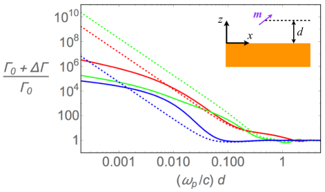
Figure 1: The spontaneous emission rate near the dielectric - conductor interface, for the
system, ref:nmat as a function of the distance from the emitter to the surface (see
the inset). The emission rate is normalized to its value in infinite dielectric . Solid lines show the exact solution obtained in the present work, while the corresponding dotted lines represent the results of the calculation based on the local theory.
Different colors corresponds to different frequencies and emission polarizations: dipole moment at (red), at (green), at (blue), where is the surface plasmon resonance frequency and is a unit vector along the normal to the interface. In this calculation, the electron scattering time , the crystal lattice permittivity of the conductor , the permittivity of the dielectric , and the Fermi velocity ; for the plasma wavelength these parameters correspond to the material system of Ref. ref:nmat
The electromagnetic field in the system defined by the self-consistent solution of the kinetic equation and the surface scattering boundary condition together with the Maxwell equations, where the electron charge and current densities are given by
(6)
(7)
Following the mathematical approach described in Ref. ENarxiv , this problem can be solved exactly, and for the reflection coefficient in the -polarization we obtain
(8)
where
(9)
For a degenerate electron gas the integration in (9) yields
(10)
with
(11)
where is the electron Fermi velocity, is the “background” permittivity of the crystal lattice in the conductor, and is the standard plasma frequency.Maier-book Note that the expression in Eqn. (10) is consistent with the other models of nonlocal free carriers response used in the recent literature. Stockman ; Khurgin
For the -polarization, we find
(12)
where
(13)
and
(14)
(15)
For a degenerate electron gas, footnote3 analytical integration over the electron momentum reduces Eqns. (14),(15) to
(18)
where
(19)
Together, Eqns. (12) and (18)-(19) define the reflection coefficient .
The resulting spontaneous emission rate can be calculated by substituting our analytical expressions for the reflection coefficients and into the general equation (2). In Fig. 1 we compare the resulting values (solid lines) with the predictions of the standard local theory (dashed lines) that describes the conductor as an effective medium with the (Drude) permittivity . Note that, as the distance to the interface is reduced, local approximation initially underestimates the density of states. This is consistent with the results of the existing non-local theories. Stockman However, at a smaller distance , this behavior is reversed: the actual density of states is now smaller than the local estimate. This is the result of the hyperbolic blockade introduced in the present work: the hyperbolic layer “blocks” the coupling to conventional surface plasmon-polaritons, and the photonic density of states is reduced. Also note strong frequency dependence of : the distance corresponding to the cross-over between the two different regimes, non-monotonically changes with the electromagnetic wavelength.
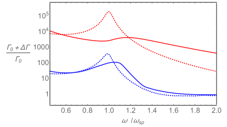
The frequency dependence of the spontaneous emission rate for a given distance to the interface, presented in Fig. 2, shows further evidence of the hyperbolic blockade. Note the suppression of the plasmon resonance, especially at the smaller distance to the interface. Furthermore, the coupling to hyper-plasmons – the new surface waves that originate from the hyperbolic layer, ENarxiv manifests itself in the enhancement of the spontaneous emission rate, seen in Fig. 2 at higher frequencies.
When the distance from the emitter to the interface is much smaller than the free-space wavelength, ,
the analytical expression for the spontaneous emission rate can be reduced to
(20)
where is related to the incomplete gamma-funciton of -th order
(21)
and
(22)
with
(23)
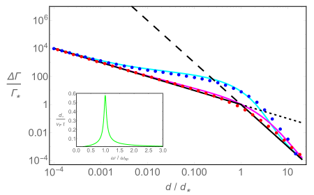
In Fig. 3, we compare the predictions of Eqn. (20) (colored lines) with the corresponding results of
the exact calculations (colored dots), as functions of the distance to the interface, for two different frequencies. Note excellent agreement in the entire parameter range shown in the figure.
Figure 2: The frequency dependence of the spontaneous emission rate near the conductor-dielectric interface. As in Fig. 1, solid lines show the exact solution, while the dotted curves correspond to the calculations using the local response model, for at (red) and (blue). The material parameters are the same as in Fig. 1. Note the suppression of the plasmon resonance due to the hyperbolic blockage, together with and order of magnitude the enhancement of the spontaneous emission rate above the plasmon resonance frequency seen at smaller distance to the interface.
Depending on the relative value of the distance and the “electronic” scale
, the analytical expression (21) has the limiting behavior
(26)
where
(27)
and
(28)
Eqn. (20) can therefore be further approximated by the interpolating function
(31)
where
(32)
and
(33)
Here, is described by the standard expression for the frequency of the surface plasmon resonance at the planar interface of a dielectric with Drude metal, .
The solid black line in Fig. 3 plots Eqn. (31), while the dashed and dotted lines correspond to and respectively. Although not sufficiently accurate at the quantitative level, the interpolation (31) correctly represents the qualitative behavior of the spontaneous emission rate and adequately describes the cross-over between the two regimes.
The inset of Fig. 3 shows the frequency dependence of the hyperbolic layer thickness . Note its non-monotonic behavior, noticed earlier in the context of the general behavior of the spontaneous emission rate as a function of the distance to the interface (see Fig. 1). The regime corresponds to the suppression of the
plasmon resonance due to the hyperbolic blockade. Except for when , as a function of frequency behaves as at and as for , with the characteristic scale given by the Thomas-Fermi screening length . For a good metal, in the optical range is on the order of a nanometer, which makes the limit essentially inaccessible. On the other hand, in transparent conducting oxides such as the ITO Sasha_review or in doped semiconductors,ref:nmat ; Wasserman2015 we find on the order of a few tens of nanometers – and the regime corresponds to the common situation of an active quantum well in a close proximity to a doped semiconductor substrate. In this case, the phenomenon of the hyperbolic blockade and the theory introduced in the present work, are essential for the accurate account of light emission from such systems.
Figure 3: The spontaneous emission rate as a function of the distance to the interface, in scaled coordinates. Red dots and the red curve correspond to the exact solution and the approximation of Eqn. (20) for , while blue dots and the blue curve show the exact solution and the approximation of Eqn. (20) for . The dipole moment . Solid black line corresponds to the interpolation (31), with the black dotted and dashed lines indicating the and limits of the exact solution. The inset shows the frequency variation of .
This work was partially supported by the National Science Foundation (grant 1629276-DMR), Army Research Office (grant W911NF-14-1-0639) and Gordon and Betty Moore Foundation.
References
(1)
S. A. Maier, Plasmonics: Fundamentals and Applications, (Springer; 1st edition, 2007).
(2)
G. W.Ford and W.H.Weber, Phys. Rep. 113, 195 (1984).
(3)
M. Moscovits, Surface-Enhanced Raman Spectroscopy: a Brief Perspective, in Surface-Enhanced Raman Scattering - Physics and Applications, edited by K. Kneipp, M. Moscovits, H. Kneipp
(Springer, 2006).
(4)
I. A. Larkin, M. I. Stockman, M. Achermann, and
V. I. Klimov, Phys. Rev. B 69, 121403(R) (2004).
(5)
G. Toscano et al, Nature Communications 6, 7132 (2015).
(6)
C. Ciraci et al, Science 337 (6098), 1072 (2012).
(7)
Y.Luo, A.I.Fernandez-Dominguez, A.Wiener, S.A.Maier, and J.B.Pendry,
Phys. Rev. Lett. 111, 093901 (2013).
(8)
J. Ziman, Electrons and Phonons: The Theory of Transport Phenomena in Solids, (Oxford University Press; reprint edition, 2001).
(9)
E. Narimanov, arXiv:1712.03484.
(10)
M. A. Noginov et al., Opt. Lett. 35 (11),
1863 (2010).
(11)
Z. Jacob, J. Y. Kim, G. V. Naik, A. Boltasseva, E. Narimanov, and V. M.
Shalaev, Appl. Phys. B 100, 215 (2010).
(12)
H. N. Krishnamoorthy, Z. Jacob, E. Narimanov, I. Kretzschmar, V. M. Menon,
Science 336 (6078), 205 (2012).
(13)
T. Galfsky, J. Gu, E. E. Narimanov and V. M. Menon, Proc. Nat. Acad. Sci. 114 (20), 5125 (2017).
(14)
L. V. Alekseyev and E. Narimanov, Radiative Decay Engineering in Metamaterials, in Tutorials in
Metamaterials, edited by M. A. Noginov, V. A. Podolskiy, (CRC Press, 2012).
(15)
K. Fuchs, Proc. Cambridge Phil. Soc. 34 (1), 100 (1938).
(16)
G. E. H. Reuter and E. H. Sondheimer,
Proc. Royal Soc. London A 195 (1042) , 336 (1948).
(17)
E.H. Sondheimer, Adv. in Phys. 1 (1), 1 (1952).
(18)
S.B. Soffer, J. Appl. Phys. 38 (4), 1710 (1967).
(19)
J. Khurgin, W.-Y. Tsai, D. P. Tsai, G. Sun, ACS Photonics 4 (11), 2871 (2017).
(20)The inequality is generally well satisfied for plasmonic materials even at room temperature: while , the Fermi energy is usually on the order of an electron-volt.
(21)
G. V. Naik, V. M. Shalaev, A. Boltasseva, 25 (24), 3264 (2013).
(22)
A. J. Hoffman et al., Nature Materials 6, 948 (2007).
(23)
Y. Zhong, S. Malagari, T. Hamilton, and D. Wasserman, J. Nanophotonics 9 (1), 093791 (2015).