Study of point- and cluster-defects in radiation-damaged silicon
Abstract
Non-ionising energy loss of radiation produces point defects and defect clusters in silicon, which result in a significant degradation of sensor performance. In this contribution results from TSC (Thermally Stimulated Current) defect spectroscopy for silicon pad diodes irradiated by electrons to fluences of a few cm-2 and energies between 3.5 and 27 MeV for isochronal annealing between 80 and 280C, are presented. A method based on SRH (Shockley-Read-Hall) statistics is introduced, which assumes that the ionisation energy of the defects in a cluster depends on the fraction of occupied traps. The difference of ionisation energy of an isolated point defect and a fully occupied cluster, , is extracted from the TSC data.
For the VOi (vacancy-oxygen interstitial) defect is found, which confirms that it is a point defect, and validates the method for point defects. For clusters made of deep acceptors the values for different defects are determined after annealing at 80C as a function of electron energy, and for the irradiation with 15 MeV electrons as a function of annealing temperature. For the irradiation with 3.5 MeV electrons the value is found, whereas for the electron energies of 6 to 27 MeV . This agrees with the expected threshold of about 5 MeV for cluster formation by electrons. The values determined as a function of annealing temperature show that the annealing rate is different for different defects. A naive diffusion model is used to estimate the temperature dependencies of the diffusion of the defects in the clusters.
keywords:
Silicon detectors , radiation damage , Shockley-Reed-Hall statistics , point defects , cluster defects , defect diffusion1 Introduction
Bulk-radiation damage in silicon limits the use of silicon detectors in high-radiation environments like at the CERN-LHC or in space. Although both microscopic and macroscopic effects of bulk damage are qualitatively understood, in spite of claims to the contrary, a consistent quantitative description of the data available has not yet been achieved. However, this is required for reliably predicting the sensor performance as a function of particle type and fluence, sensor design and operating parameters. The reason is that the number of radiation-induced states in the silicon band gap is large (see figure 1), their properties are frequently only poorly known, and effective states [1] have to be used in simulations because of the large number of defects. In addition, a quantitative understanding of defect clusters is lacking and in the TCAD simulations they are approximated by point defects.
In this contribution we propose a simple, physics motivated parametrization of the properties of cluster defects and apply it to spectroscopic results from TSC (Thermally Stimulated Current) measurements. We present results for silicon irradiated with electrons of 3.5 to 27 MeV kinetic energy [2, 3]. As the threshold for defect cluster production is expected to be around 5 MeV for electrons [4], these data are well suited to check the validity of the method.
In the present work single vacancy related defects are considered to be point-like defects (e. g. the VOi defect). Such isolated point defects are produced in silicon by low energy recoils, whereas an agglomeration of defects (or a cluster for short) results from high energy recoils that introduce a dense cascade of silicon atoms displaced from their original lattice position.
2 Test Structures and Measurements
For the studies p+n n+ pad diodes, produced on 283 m thick float-zone n-type silicon with a phosphorous-doping of approximately 1012 cm-3 and an oxygen concentration cm-3, were used. The p+ implant of 25 mm2 area is surrounded by a guard ring. A window in the aluminum on top of the p+ implant with the shape of a decagon and an area of 3.25 mm2 allows to inject light through the p+ contact. The n+ back contact is covered by an aluminum grid.
The pad diodes have been irradiated with electrons of , 6, 15, and 27 MeV to fluences between 1 and cm-2. For the sample irradiated with 15 MeV electrons, TSC measurements were performed before and after isochronal annealing for 30 min at temperatures C, in 20C steps. At the other energies, data were only taken before and after annealing of 30 min at C. For the TSC measurements the bias was applied to the back n+ contact, and both p+ contact and guard ring were at ground potential.
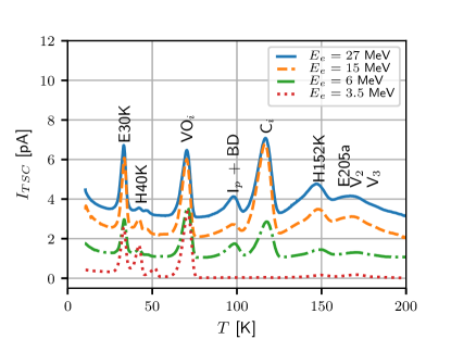
Figure 1 shows typical TSC spectra of pad diodes irradiated by electrons of different energies after 30 min annealing at 80C. Trap filling has been applied at K with a forward-current of approximately 1 mA, so that both electron- and hole-traps are filled and contribute to the TSC spectra. The heating rate was K/s. For more details we refer to [2, 5, 6]. In the following we will limit the discussion to the point defect VOi (vacancy-oxygen interstitial) at 70 K and to the states in the K region, which are known to be cluster defects and have a significant impact on the sensor performance [7].
For the TSC measurements analysed in this paper, the diodes were cooled to K at 200 V reverse bias to assure empty traps. At the temperature the traps were filled with electrons by injecting light of 520 nm through the 3.25 mm2 window of the p+ contact, and the current, , released by the traps was recorded as a function of for a constant heating rate K/s. As a result of the light injection, only electron traps are filled and only the charges released from electron traps contribute to (see figure 2).
3 Analysis Method
According to SRH statistics [8, 9] the temperature dependence of the TSC current, , from acceptor states at an energy from the conduction band, which are filled with electrons at the temperature to the concentration , is given by:
| (1) |
| (2) |
| (3) |
with the elementary charge , the diode volume where the traps have been filled , the emission rate , the ratio of filled states at the temperature relative to , , the thermal velocity of electrons , the electron capture cross-section , and the density of states at the conduction band . For these quantities the default values of Synopsys TCAD [10], in particular the relation of [11], are used. The effective thermal electron mass , with the Boltzmann constant and the free electron mass .
For point defects a constant value for is expected. As proposed in [12], cluster defects can be characterized by an occupation-dependent value of . For the dependence , i. e. the change of the ionisation energy with the fraction of defects filled in a cluster, a linear dependence is assumed:
| (4) |
The schematic drawing of figure 3 shows the potential energies of electrons in a cluster of 15 equally spaced electron traps on a straight line. The full dots correspond to , when all 15 traps are filled with electrons. The empty circles is the situation , when only a single trap is filled and the energy is equal to the energy of the single isolated trap. The ionisation energy is minimal for , and reaches its maximum , the value for point defects, for .
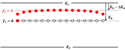
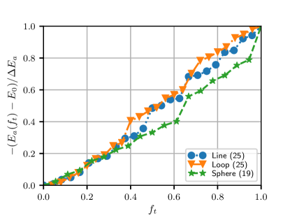
Figure 4 shows the results of simple, electrostatic simulations of the dependence of . For Line (25) the cluster is assumed to be a straight line of 25 equally spaced point defects, fixed in space. The energy difference between the conduction band and a single point defect is . In the initial state, , each point defect is occupied by an electron and negatively charged. The point defect with the highest (negative) potential energy, , and thus the lowest value, , is discharged first, when the temperature is raised in the TSC measurement. Next, the point defect with the lowest value for the new charge configuration is found and discharged. This chain is continued, until all defects are discharged. The cluster Loop (25) consists of 25 equally spaced point defects on a circle, and Sphere (19) of 19 point defects in a sphere on a 3-D Cartesian grid. Figure 4 shows that to a good approximation for all three topologies, is linear in . Loop clusters are discussed in [12], which actually triggered our studies.
The data analysis consists in subtracting from the measured TSC current the dark current, obtained from the TSC measurement without trap filling. Then -fits of eq. 1 for different intervals are performed. For the errors 1 % times the measured currents have been assumed, which takes into account the uncertainty of the current measurement as well as the accuracy of the temperature regulation of the TSC setup. The free parameters of the model are , , and for each defect, where is the density of point defects per volume, which are filled in the experiment at , i. e. the product of cluster density times the number of filled point defects in a cluster.
4 Results
4.1 The VOi defect
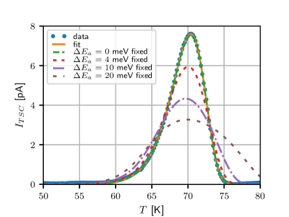
As a first step, the vacancy-oxygen (VOi) defect located at approximately K is investigated. The VOi is known to be a point defect. According to reference [13] it is an electron trap with an energy meV from the conduction band and an electron capture cross-section cm-2. The values in reference [14] are meV and cm-2. In figure 5 the TSC data after electron irradiation with MeV to the fluence cm-2 and 30 min annealing at C are shown as dots. The fit results are shown as a solid line, and the parameters are given in table 1. For the assumed 1 % uncertainty for the measurement, a for degrees of freedom is found. We note that the differences fit – measured are dominated by the systematics of the temperature regulation and not by the statistical fluctuations of the current measurement. The values meV and cm-2 (statistical errors only) differ significantly from the values given in [13]. If meV is assumed, the increases to 61 and cm2 is obtained. However, the value of meV is incompatible with zero, the value expected for a point defect. For the remaining curves of figure 5 the value meV is assumed and is fixed to the values given in the insert. Values significantly larger than zero are incompatible with the data. We conclude that values, which differ significantly from zero are excluded.
| [meV] | [meV] | [cm-3] | [cm2] | |
|---|---|---|---|---|
| 25/47 | ||||
| 176 | 61/48 |
The data after irradiation by electrons with energies between 3.5 and 15 MeV and after 30 min annealing at 80C, have also been analysed. In all cases, values close to zero and consistent values for and are obtained. This confirms that VOi is a point defect, and validates the analysis method for an isolated point defect.
4.2 Cluster defects
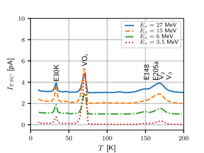
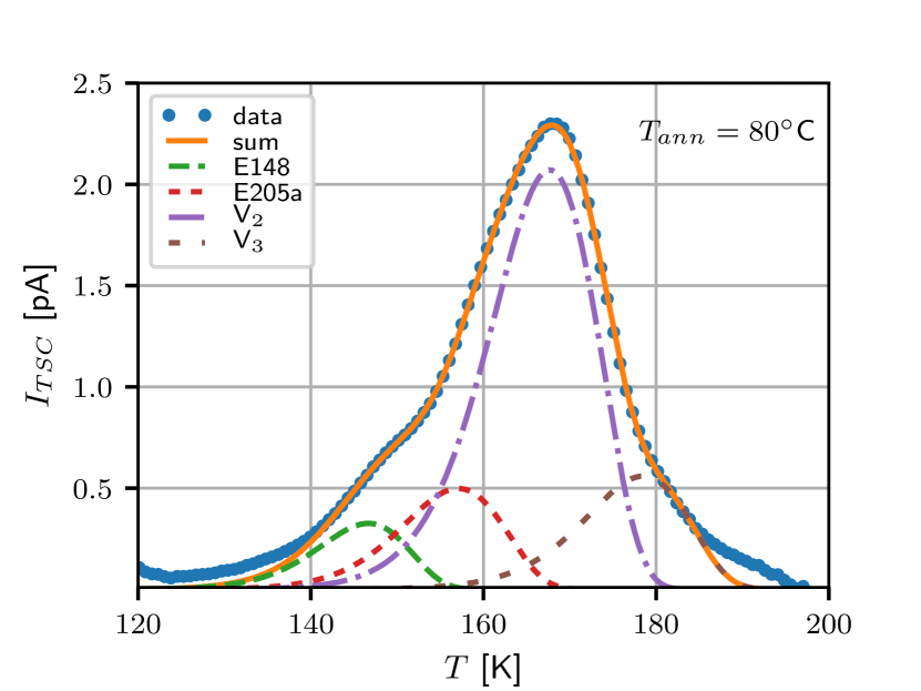
Next, the region K is investigated, where overlapping defect clusters are located, which are responsible for part of the generation current, charge trapping and changes in the effective space-charge density [3]. The TSC spectra for the irradiations at the different values after 30 min annealing at 80C are shown in fig. 6.
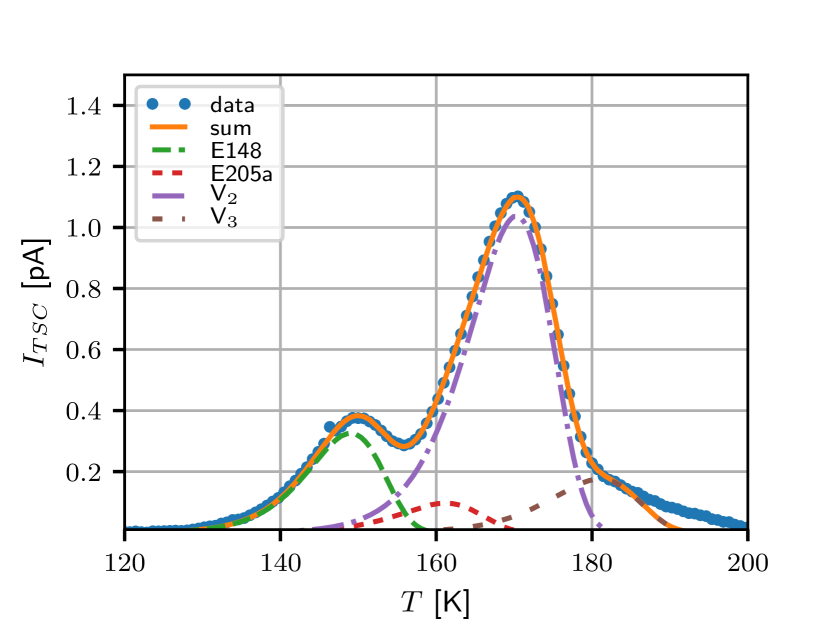
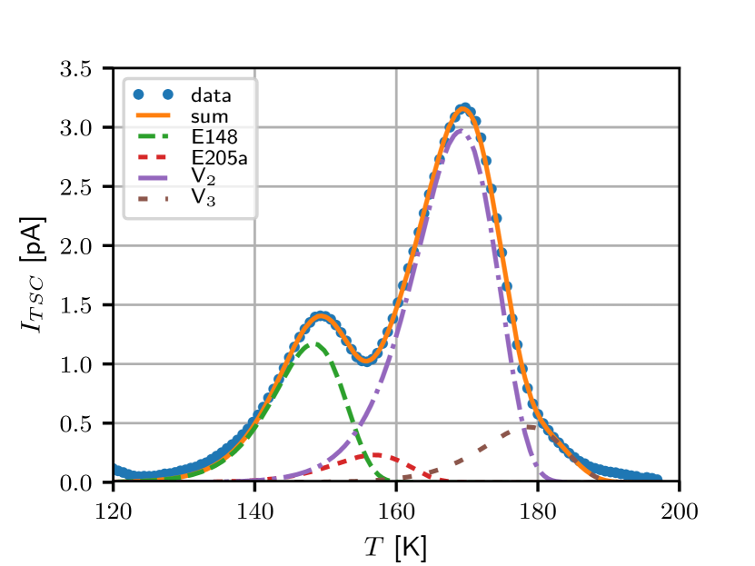
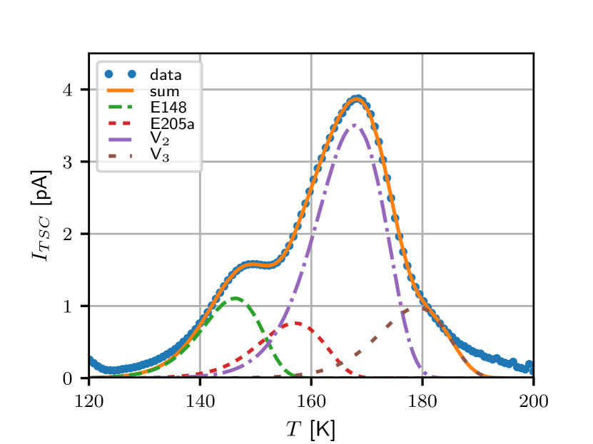
To describe the data, four defects have been assumed: the di-vacancy V2, the tri-vacancy V3 and two additional defects, E148 and E205a. The values of from the literature are given in table 2. Using eq. 1 the sums of the contributions of all four defects have been fitted to the measurements. In the fit, the literature values for , a value common for the two defects E148 and V3, and another value common for E205a and V2, have been assumed. Other assumptions, e. g. a common value for all 4 states, gave qualitatively similar results. Without such constraints, which are only poorly motivated, the fits do not converge to stable results. Figure 6 compares the fit results to the data, and table 2 shows as an example the parameters derived for the MeV data. The TSC spectra are well described by the fits. It has been verified that they cannot be described with acceptable trap parameters if is assumed, and conclude that the model with an occupation-dependent ionisation energy provides a good description of the TSC spectra of the cluster defects.
| Defect | [meV] | Ref. | [meV] | / [cm | / [cm2] |
|---|---|---|---|---|---|
| E148 | 359 | [5, 15] | 4.3 | 0.33 | 4.6 |
| E205a | 393 | [5, 13] | 7.6 | 0.56 | 6.1 |
| V2() | 424 | [13] | 7.6 | 2.44 | 7.0 |
| V3() | 456 | [3, 13] | 4.3 | 0.65 | 9.7 |
In order to investigate the dependence of the cluster formation on the electron energy, , figure 7 shows for the V3/E148 and the V2/E205a clusters obtained from the fits described above. The values for MeV are compatible with zero. For higher electron energies the values differ significantly from zero and the energy dependence is as expected for a threshold of cluster formation in the region MeV.
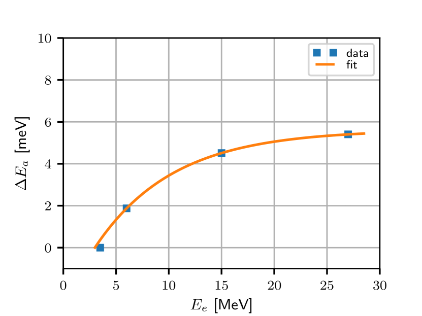
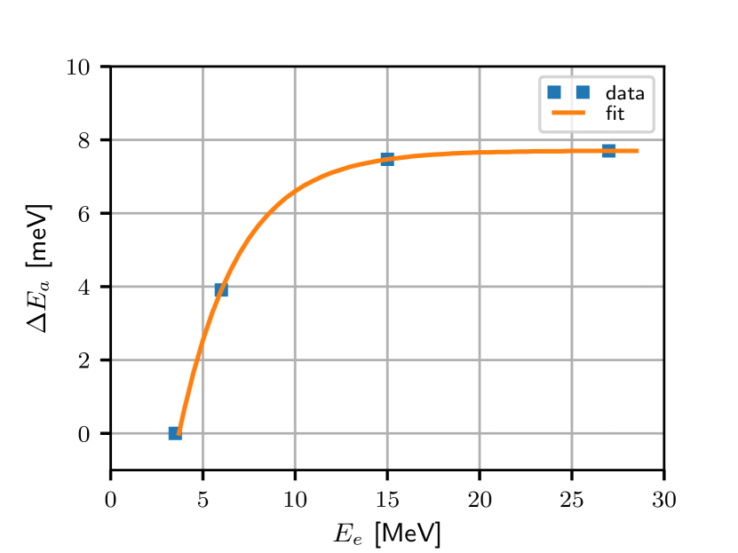
The phenomenological function with the free parameters , and ,
| (5) |
is fit to the data. For the threshold values MeV and MeV are obtained.
We note that for the models presented in section 3, a value of meV corresponds to a spacing of about 100 nm of the point defects, which are filled at K in the clusters, to be compared to the silicon-lattice constant of 0.543 nm at 300 K. The values are compatible with simulations of electron-induced damage in silicon, which take into account the Mott cross-section, the vacancy and interstitial generation, as well as their diffusion and recombination [16].
4.3 Cluster annealing
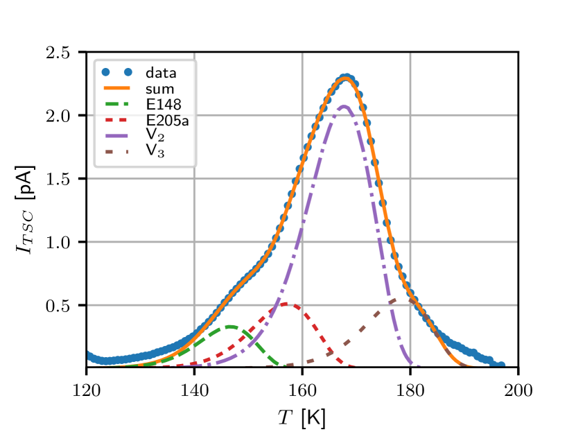
In the following, the analysis of the data for the irradiation with MeV for the conditions as irradiated and after isochronal annealing for C in 20C steps and 30 min annealing time, is presented. The temperature history for as irradiated is only approximately known: After the 15 MeV irradiation at Dresden-Rossendorf the diode had been at room temperature for about eight hours during the transport to Hamburg, where it has been stored in the freezer at C. In the following this condition is labeled C. In figure 8 we show as examples the comparison of the fit results with the measurements for as irradiated and after the isochronal annealing steps of 80C, 180C and 280C. For the fits the assumptions discussed in section 4.2 are made. For all values the data are well described by the model.
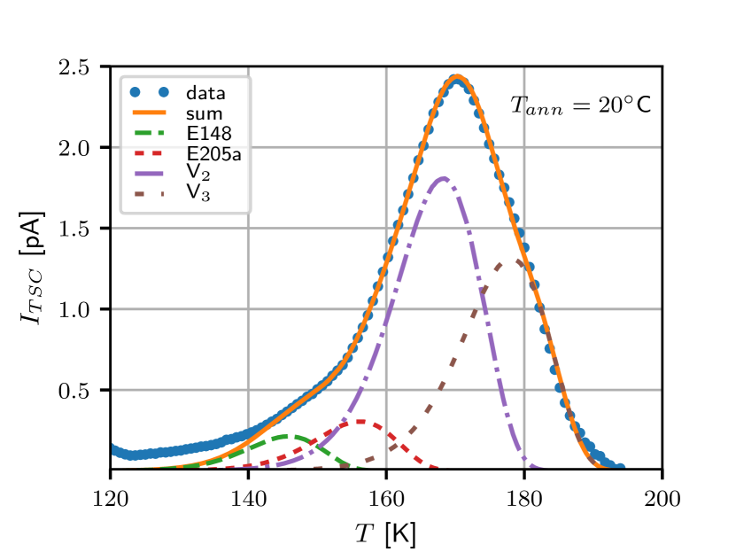
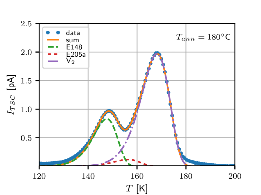
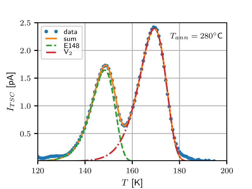
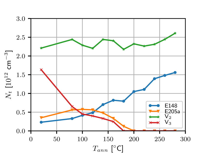
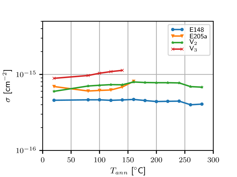
The results for of the four defects, and the cross-sections for electrons, , as a function of are shown in figure 9. As discussed in section 3, is not the density of filled clusters, but the product of the cluster density times the number of filled traps in the cluster. We observe that with increasing annealing temperature remains constant for V2, increases for E148, and vanishes for V3 and for E205a. More details on the annealing behavior of and E205a can be found in [5]. As expected the electron cross-sections do not depend on .
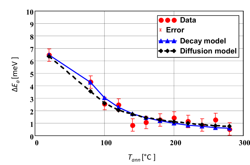
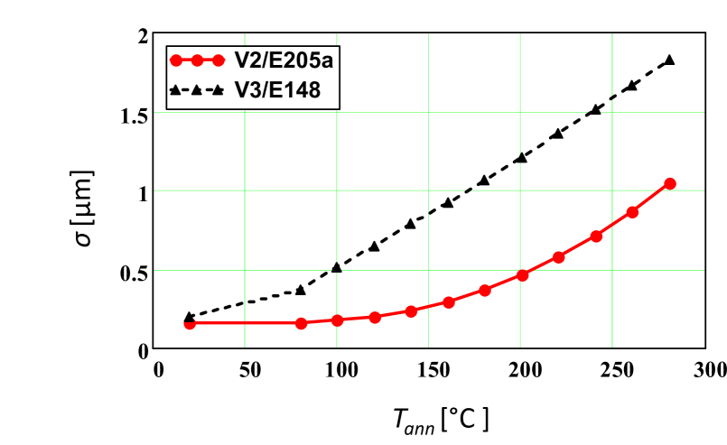
The results for as a function of for the traps V2/E205a and V3/E148 are shown in figure 10. For V2/E205a the value of remains nearly constant ( meV) for the annealing at C, then decreases to meV above C.
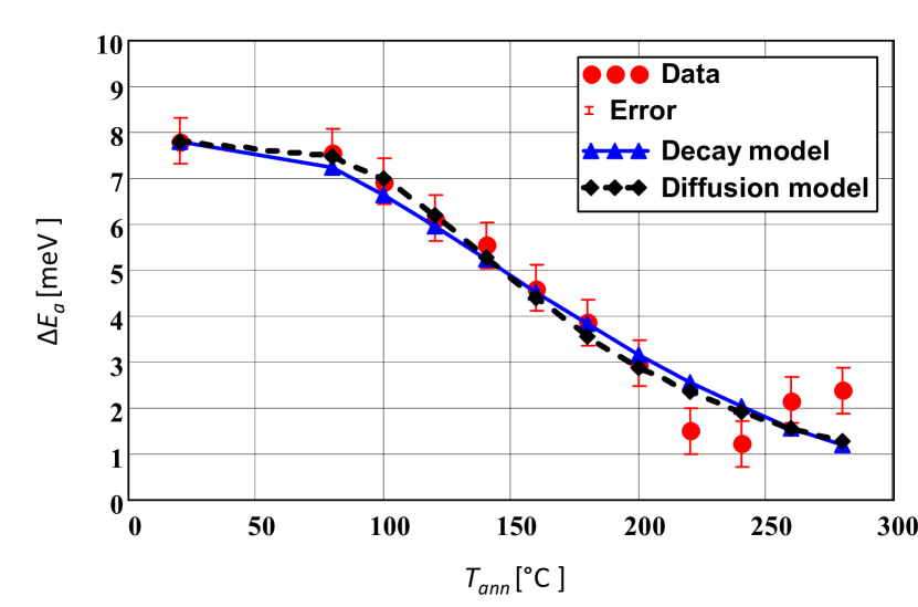
For V3/E148 the decrease of with is significantly faster, and a constant value of meV is reached at C. For the description of two models are introduced: a first order decay model, and a diffusion model.
The first order decay model uses the following formula for after the -th annealing step
| (6) |
with the annealing time min. The first order process is described by the frequency factor and the activation energy . For the as irradiated data assigned to C are used. The results of the fits to the data are shown in figure 10 and in table 3. The model provides an acceptable description of the data.
The diffusion model follows a similar approach as the model discussed in section 3, which was used to derive the linear dependence of the ionisation energy on the fraction of occupied defects. Each cluster is assumed to consist of point defects, which diffuse during the annealing steps. For the temperature dependence of the diffusion constant the standard parametrisation
| (7) |
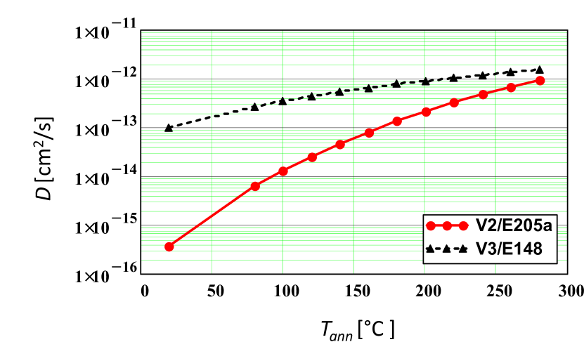
is used. The activation energy for the diffusion of the point defects in the cluster is , and a constant. For the fit clusters with point defects each, are generated. The position of the -th point defect in the -th cluster after the -st annealing step is denoted by . The position after the -th annealing step is , where is a vector of three Gauss-distributed random numbers with width . Assuming that all point defects are occupied by electrons, the individual potential energies are calculated. The biggest is assumed to be the value of the -th cluster, and the average of the clusters is fitted to the data. The initial positions of the point charges in the are generated as points spaced by on a straight line each smeared with a vector of three Gauss-distributed random numbers with width . For a given number of clusters, , and cluster size, , the free parameters of the fit are , , and . For the fits to the data shown in figure 10, and are used. Fits have also been performed for other values. The values obtained depend only weakly on and there is a shallow minimum around . The parameters obtained from the fit are given in table 4, where the diffusion constants at 423.15 K, , instead of are shown. Using the value of at the average annealing temperature 423.15 K has the advantage that and are essentially uncorrelated. In addition, it is more easily interpreted than , which corresponds to the value of for .
We note that, whereas the values of the parameters given in table 4 change significantly if the fit region is changed, the dependencies of and , shown in figure 11, are much less affected. The values of the diffusion activation energy eV for V2/E205a is similar to the value given in [17] for the vacancies V0 and V-1, and eV for V3/E148 similar to the interstitial Si.
| Defect | [1/s] | [eV] | Fit range [∘C] | |
|---|---|---|---|---|
| V2/E205a | 0.113 | 15.6/10 | ||
| V2/E205a | 0.225 | 1.2/8 | ||
| V3/E148 | 7.9/10 | |||
| V3/E148 | 0.014 | 2.3/3 |
| Defect | [nm2/s] | [eV] | [nm] | [nm] | [∘C] | |
|---|---|---|---|---|---|---|
| V2/E205a | 6.3 | 0.423 | 27 | 159 | 6.4/8 | |
| V3/E148 | 60 | 0.146 | 27 | 200 | 5.7/8 |
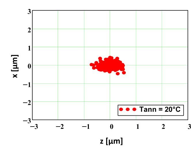
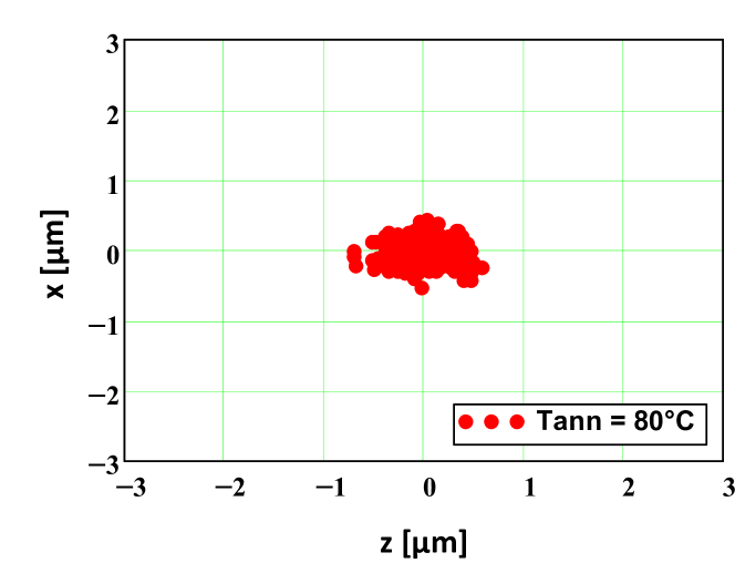
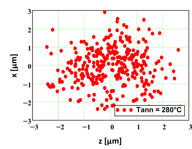
As a pictorial presentation of the diffusion of the point defects in the clusters, figure 12 shows for the V2/E205a cluster the distribution of the superposition of 20 cluster with 15 point defects each, using the parameters of table 4 for the conditions as irradiated, and after the annealing steps , and 280C. The point defects of the initial cluster, which are separated by the distance , are generated along the direction. As expected from figure 11(b), hardly any diffusion is observed at C, the width increases by about a factor 3 at 180C, and the clusters are essentially dissociated at 280C. We note that for cm-3, shown in figure 9(a), and 15 point defects in each cluster, the average distance between clusters is m.
We now summarise the results of the two models used to describe the annealing measurements: Both models provide a description of the dependence for the V2/E205a and the V3/E148 clusters. Whereas the first order decay model is a purely phenomenological parametrisation, the diffusion model is physics based and gives, within the assumptions made to determine the values and the limitation of this simple model, insight into the cluster annealing. The diffusion-activation energy, , is quite different for the two cluster defects: eV for V2/E205a and eV for V3/E148. At an annealing temperature of 80C the diffusion parameter, , for V2/E205a is about a factor 50 smaller than for V3/E148. However at 280C, the highest annealing temperature investigated, they are quite similar. As a consequence, the diffusion of the point defects in the V3/E148 cluster becomes significant only for temperatures above 150C, whereas for the V2/E205a cluster it is already significant at room temperature. At the highest annealing temperatures the spread of the points in the cluster approaches the average distance between the clusters.
5 Conclusions
In this paper a new method of analyzing TSC (Thermally Stimulated Current) spectra of radiation-damaged silicon diodes is presented. It is based on the Shockley-Read-Hall statistics and can be used to describe both point and cluster defects. An ionisation energy, , which depends on , the fraction of filled point defects in the cluster, is introduced. Simple electrostatic model calculations show that a linear dependence appears to be a reasonable approximation, where is the ionisation energy of the point defect which makes up the cluster, and the difference in ionisation energy between and . The method is applied to the analysis of TSC spectra from n-type silicon diodes irradiated by electrons in the energy range between 3.5 and 27 MeV. For the filling of the traps the the p+ implants of the diodes are exposed to green light, so that only acceptor traps contribute to the TSC current.
As a first step the VOi defect (an electron trap with eV, which is known to be a point defect) is analysed for the diode irradiated by 27 MeV electrons to a fluence of cm-2. The value found for is compatible with zero. This confirms that VOi is a point defect, and also demonstrates the validity of the method for point defects.
Next, the radiation-induced deep acceptor states with energies between 0.35 and 0.46 eV from the conduction band are investigated. They are responsible for part of the generation current, for charge trapping and for changes of the effective space-charge density with irradiation. In the analysis it is assumed that four defects, E148, E205a, V2, and V3 contribute to the TSC current in this energy region. For the fits to the TSC spectra, the ionisation energies from the literature and common values for V2 and E205a as well as for V3 and E148 had to be assumed. Without these or similar not too well justified assumptions, the fits do not converge to stable values.
To study the dependence of the cluster formation on electron energy, the data for , 6, 15, and 27 MeV after annealing for 30 min at 80C are analysed. For the lowest electron energy , whereas for the higher electron energies positive values are found. After a rapid increase with electron energy, a tendency towards a saturation of is observed. This is taken as evidence for cluster formation above a threshold, which is somewhere between MeV.
To study the annealing of the clusters, the data for the irradiation with 15 MeV electrons and the conditions as irradiated and after isochronal annealing for 30 min between C are analysed with the assumptions discussed above. For both V2/E205 and V3/E148, is found to decrease with , however the decrease for V3/E148 is significantly faster than for V2/E205. Two models, a first order decay model and a diffusion model, provide adequate descriptions of the data. Using the latter model the dependence of the diffusion parameters and of the spatial spread of the point defects in the cluster is estimated. It is found, that at C the diffusion constant for V2/E205a is about a factor 50 smaller than for V3/E148, whereas at C, they are quite similar. For the diffusion-activation energy, , a value of 0.42 eV is determined for the V2/E205 cluster, and 0.15 eV for the V3/148 cluster. For the highest values, the spread of the point defects in the clusters approaches the average distance between the clusters.
6 Acknowledgements
This work has been performed in the framework of the CERN-RD50 collaboration and PNII-ID-PCE-2011-3 Nr. 72/5.10.2011, and partially funded by CiS, the German BMBF and the Helmholtz Alliance Physics at the Terascale. I. Pintilie and R. Radu gratefully acknowledge partial funding from the Romanian core program PN18-11 (funded by ANCSI). R. Radu was also partially supported by the Marie Curie Initial Training Network MC-PAD and the fellowship A127881 of the German Academic Exchange Service (DAAD). We also thank the teams at the irradiation facilities at the Belarusian State University at Minsk, the PTB at Braunschweig, and the ELBE accelerator at Dresden-Rossendorf, where the irradiations have been performed. We are grateful to P. Buhmann and M. Matysek for maintaining the measurement infrastructure of the Hamburg Detector Laboratory, where the measurements were performed, in an excellent shape.
7 References
References
- [1] V. Eremin, E. Verbitskaya, Z. Li, The origin of double peak electric field distribution in heavily irradiated silicon detectors, Nucl. Instr. & Meth. A 476, 556 (2002).
- [2] R. Radu et al., Radiation damage in n-type silicon diodes after electron irradiation with energies between 1.5 MeV and 15 MeV, Nucl. Instr. & Meth. in Phys. Res. A 730, 84 (2013).
- [3] R. Radu et al., Investigation of point and extended defects in electron irradiated silicon: dependence on the particle energy, J. Appl. Phys. 117, 164503 (2015).
- [4] V. A. J. Lint, T. M. Flanagan, R. E. Leadon, J. A. Naber, and V. C. Rogers, Mechanisms of Radiation Effects in Electronic Materials, Vol. 1, John Wiley & Sons, Inc. (1980); p. 272 and p. 286.
- [5] A. Junkes, Influence of radiation induced defect clusters on silicon particle detectors, PhD Thesis, Hamburg University, DESY-THESIS-2011-031.
- [6] I. Pintilie et al., Stable radiation induced donor generation and its influence on the radiation tolerance of silicon diodes, Nucl. Instr. & Meth. in Phys. Res. A 556, 197 (2006).
- [7] I. Pintilie et al., Cluster related hole traps with enhanced-field-emission - the source for long term annealing in hadron irradiated Si diodes, Appl. Phys. Lett. 92, 024101 (2008).
- [8] W. Shockley and W. T. Read, Statistics of the recombinations of holes and electrons, Phys. Rev. 87, 835 (1952).
- [9] R. N. Hall, Electron-hole recombination in germanium, Phys. Rev. 87, 387 (1952).
- [10] Synopsys TCAD web-page, http:www.synopsys.com.
- [11] M. A. Green, Intrinsic concentration, effective densities of states, and effective mass in silicon, J. Appl. Physics, vol. 67-6, 2944–2954 (1990).
- [12] A. Scheinemann and A. Schenk, TCAD-based DLTS simulation for analysis of extended defects, Phys. Stat. Sol. A 2111, 136 (2014).
- [13] M. Moll, Radiation damage in silicon particle detectors, PhD Thesis, Hamburg University, DESY-THESIS-1999-040.
- [14] S. D. Brotherton and P. Bradley, Defect production and lifetime control in electron and -irradiated silicon, J. Appl. Physics, vol. 53-8, 5720 (1982).
- [15] I. Pintilie et al., Thermally stimulated current method applied to diodes with high concentration of deep trapping levels, Applied Physics Letters, vol. 78-4, 550 (2001).
- [16] G. Lindstroem and G. Kramberger, Electron Induced Damage in Silicon, presentation at the 24th RD50 Workshop, Bucharest 1113 June 2014, unpublished.
- [17] S. M. Myers P. J. Cooper and W. R. Wampler, Model of defect reactions and the influence of clustering in pulse-neutron-irradiated Si, J. Appl. Physics 104, 044507 (2008).