Biaxial strain tuned electronic structures and power factor in Janus Transition Metal Dichalchogenide monolayers
Abstract
Tuning physical properties of transition metal dichalcogenide (TMD) monolayers by strain engineering have most widely studied, and recently Janus TMD monolayer MoSSe has been synthesized. In this work, we systematically study biaxial strain dependence of electronic structures and transport properties of Janus TMD MXY (M = Mo or W, X/Y = S, Se, or Te) monolayer by using generalized gradient approximation (GGA) plus spin-orbit coupling (SOC). It is found that SOC has a noteworthy detrimental influence on power factor in p-type MoSSe, WSSe, n-type WSTe, p-type MoSeTe and WSeTe, and has a negligible influence on one in n-type MoSSe, MoSTe, p-type WSTe and n-type MoSeTe. These can be understood by considering SOC effects on their valence and conduction bands. For all six monolayers, the energy band gap firstly increases, and then decreases, when strain changes from compressive one to tensile one. It is found that strain can tune strength of bands convergence of both valence and conduction bands by changing the numbers and relative position of valence band extrema (VBE) or conduction band extrema (CBE), which can produce very important effects on their electronic transport properties. By applying appropriate compressive or tensile strain, both n- or p-type Seebeck coefficient can be enhanced by strain-induced band convergence, and then the power factor can be improved. Our works further enrich studies on strain dependence of electronic structures and transport properties of new-style TMD monolayers, and motivate farther experimental works.
pacs:
72.15.Jf, 71.20.-b, 71.70.Ej, 79.10.-n Email:sandongyuwang@163.comI Introduction
Due to direct hot-electricity conversion without moving parts, thermoelectric materials have enormous potential to solve energy issues, and the efficiency of thermoelectric conversion can be measured by the dimensionless figure of merits1 ; s2 , , in which S is the Seebeck coefficient, is electrical conductivity, T is absolute temperature, and are the electronic and lattice thermal conductivities, respectively. Based on the expression of , an excellent efficiency of thermoelectric conversion requires high power factor () and low thermal conductivity (). However, the S and are oppositely proportional to the carrier concentration. Due to simultaneously increasing and decreasing , low-dimensional materials may have potential advantages in improving q1 ; q2 ; q3 .
Since the discovery of grapheneq6 , two-dimensional (2D) materials have been attracting increasing attention, such as TMD, group-VA, group IV-VI and group-IV monolayersq7 ; q8 ; q9 ; q10 ; q11 . The heat transport properties of these 2D materials have been widely studied, such as TMD, orthorhombic group IV-VI, group-VA, , ATeI (A=Sb or Bi) and monolayers q12 ; q13 ; q14 ; q15 ; q16 ; q17 ; q18 ; q19 . In semiconducting TMD monolayers (M=Zr, Hf, Mo, W or Pt; X=S, Se, or Te), the SOC is proved to be very important for electronic transport propertiesq20 . Strain effects on the electronic structures and heat transport properties of TMD monolayers have been widely investigated both in theory and experiment. A semiconductor-to-metal transition can be observed by a small compressive strain (about 3%) in , compared with with very large strainq21 ; q21-1 . For , the significantly enhanced power factor can be observed in n(p)-type doping by compressive (tensile) strain at the critical strain of direct-indirect gap transitionq21-2 . It is found that tensile strain can improve thermoelectric properties of , and by enhancing and reducing q21 ; q22 ; q23 .

Recently, Janus monolayer MoSSe has been experimentally achieved by breaking the out-of-plane structural symmetry of , replacing the top S atomic layer with Se atomsp1 . It is found that Janus MoSSe monolayer can be used as a potential wide solar-spectrum water-splitting photocatalyst with a low carrier recombination ratep1-1 . In monolayer and multilayer Janus TMD MXY (M = Mo or W, X/Y = S, Se, or Te), the strong piezoelectric effects have been observed by first-principles calculationsp2 . It is found that the carrier mobility in monolayer MoSSe is relatively low, but the bilayer or trilayer structures show a quite high electron/hole carrier mobilityp2-1 . Electronic and optical properties have been investigated in pristine Janus MoSSe and WSSe monolayers, as well as their vertical and lateral heterostructuresp3 . It is found that the of MoSSe monolayer is higher than that of monolayer, but is very lower than that of monolayerp4 . Calculated results show that ZrSSe monolayer predicted with the 1T phase has better n-type thermoelectric properties than monolayer p4-1 .
In this work, the biaxial strain dependence of electronic structures and transport properties of Janus TMD MXY (M = Mo or W, X/Y = S, Se, or Te) monolayers are studied by first-principles calculations and Boltzmann equation. It is very crucial for Janus TMD monolayers to include SOC for attaining reliable electronic structures and transport properties, which is similar with TMD monolayersq20 ; q21 ; q21-2 . For all six Janus TMD monolayers, the energy band gap shows a nonmonotonic up-and-down behavior with increasing strain, while the spin-orbit splitting at point monotonically increases. Calculated results show that strain can tune strength of bands convergence of valence (conduction) bands by changing the numbers and relative position of VBE (CBE), which can obviously affect their electronic transport properties. Both n- or p-type Seebeck coefficient can be enhanced by applying appropriate compressive or tensile strain, and then the power factor can be improved. Similar strain-improved power factor can also be found in TMD monolayersq21 ; q21-2 ; q22 ; q23 .
| Name | - | ||||
|---|---|---|---|---|---|
| MoSSe | 3.252 | 1.55 | 1.47 | 0.08 | 0.168 |
| MoSTe | 3.327 | 1.17 | 1.14 | 0.03 | 0.181 |
| MoSeTe | 3.394 | 1.34 | 1.22 | 0.12 | 0.196 |
| WSSe | 3.220 | 1.76 | 1.43 | 0.33 | 0.426 |
| WSTe | 3.325 | 1.35 | 1.21 | 0.14 | 0.396 |
| WSeTe | 3.391 | 1.67 | 1.08 | 0.59 | 0.433 |
The rest of the paper is organized as follows. In the next section, we shall describe computational details about electronic structures and transport properties. In the third section, we shall present strain dependence of the electronic structures and transports properties of Janus TMD MXY (M = Mo or W, X/Y = S, Se, or Te) monolayers. Finally, we shall give our discussions and conclusion in the fourth section.
II Computational detail
A full-potential linearized augmented-plane-waves method within the density functional theory (DFT) 1 is used to investigate strain dependence of electronic structures of MXY (M = Mo or W, X/Y = S, Se, or Te) monolayer, as implemented in the WIEN2k package2 . We employ the popular GGA of Perdew, Burke and Ernzerhof (GGA-PBE)pbe for the exchange-correlation potential, and the internal position parameters are optimized with a force standard of 2 mRy/a.u.. The SOC was included self-consistently 10 ; 11 ; 12 ; so , which can produce important effects on both electronic structure and transport coefficients. To attain reliable results, we use 5000 k-points in the first Brillouin zone (BZ) for the self-consistent calculation, make harmonic expansion up to in each of the atomic spheres, and set . The self-consistent calculations are considered to be converged when the integration of the absolute charge-density difference between the input and output electron density is less than per formula unit, where is the electron charge.
Based on calculated energy band structures, transport coefficients, such as Seebeck coefficient and electrical conductivity, are performed through solving Boltzmann transport equations within the constant scattering time approximation (CSTA) as implemented in BoltzTrapb . To achieve the convergence results, the parameter LPFAC is set to 40. The accurate transport coefficients need dense k-point meshes, and at least 2400 k-points is used in the irreducible BZ for the energy band calculation. It is noted that, for 2D material, the calculated electrical conductivity depends on the length of unit cell along z direction2dl . They should be normalized by multiplying , in which is the length of unit cell along z direction, and is the thickness of 2D material. It is well known that the is not well defined like graphene. In this work, the =20 is used as .
III MAIN CALCULATED RESULTS AND ANALYSIS
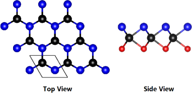
The structure of Janus MXY (M = Mo or W, X/Y = S, Se, or Te) monolayer (Figure 1) is similar to monolayer with the 2H phase, which contains three atomic sublayers with M layer sandwiched between X and Y layers. Compared with , the Janus MXY monolayer lacks the reflection symmetry with respect to the central metal M atoms. With the sandwiched S-Mo-Se structure, Janus TMD monolayer MoSSe has been experimentally achieved by replacing the top S atomic layer in with Se atomsp1 . To avoid spurious interaction between neighboring layers, the unit cell of Janus MXY monolayer, containing one M, one X and one Y atoms, is constructed with the vacuum region of more than 18 . The optimized lattice constantsp2 for MXY are listed in Table 1 using GGA.

It has been proved that SOC can produce important effects on electronic structures for (M=Zr, Hf, Mo, W or Pt; X=S, Se, or Te), and further influences their thermoelectric propertiesq20 ; q21 ; q21-2 ; q23 . Due to similar crystal structure and element type between TMD and Janus TMD monolayers, the SOC is included for all calculations of Janus TMD monolayers. Figure 2 shows the calculated energy bands for monolayer MoSSe and WSSe with GGA and GGA+SOC, and FIG.1 and FIG.2 in the Supporting Information (SI) show ones of monolayer MoSTe, WSTe, MoSeTe and WSeTe. For monolayer MoSSe, the indirect gap of 1.55 eV is calculated with valence band maximum (VBM) at point and conduction band minimum (CBM) at K point using GGA. A second maxima appears at K point, which is 0.01 eV lower than VBM. When the SOC is considered, the VBM changes from point to K point with a direct gap of 1.47 eV, and the energy difference between and K is 0.07 eV. It is noted that these results sensitively depend on lattice constants. For WSSe, the CBM is along the -K direction, and an indirect gap of 1.76 eV (1.43 eV) using GGA (GGA+SOC) is defined with the VBM at the point. For MoSTe and WSTe, the CBM and VBM are located along the -K direction and at point. The MoSeTe and WSeTe have indirect gaps with the CBM and VBM along the -K direction and at K point. The GGA gaps, GGA+SOC gaps and the differences between them are shown in Table 1. It is found that the gaps with GGA+SOC are smaller than ones with GGA for all materials, which is caused by spin-orbit splitting. It is found that the Rashba spin-orbit splitting exists at point of valence bands because of lacking the inversion symmetry. The gap difference between GGA and GGA+SOC can reflect the SOC influences on the conduction bands, and the larger gap decrease means the stronger SOC. The SOC effects on the valence bands near Fermi level can be described by spin-orbit splitting at the K point, which are summarized in Table 1. It is clearly seen that WXY has larger spin-orbit splitting than MoXY.
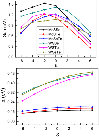
Both in theory and in experiment, strain effects on the energy band structures and transport properties of TMD monolayers have been widely investigatedq21 ; q21-2 ; q22 ; q23 ; qin1 . Here, biaxial strain effects on the electronic structures and electronic transport coefficients of MXY (M = Mo or W, X/Y = S, Se, or Te) monolayer are studied. To simulate biaxial strain, is defined, where is the unstrained lattice constant. 0 means compressive strain, while 0 implies tensile strain. Using GGA+SOC, the energy band gap and spin-orbit splitting value at K point in the valence bands around the Fermi level as a function of are plotted in Figure 3. For all materials, the energy band gap firstly increases, and then decreases, when changes from -6% to 6%. Similar strain dependence of energy band gap can also be found in TMD monolayersq21 ; q21-2 ; q22 ; q23 . As increases, the spin-orbit splitting at K point monotonically increases, and the change is 0.0270.044 eV for MoXY and 0.1640.220 eV for WXY, which means the spin-orbit splitting has stronger dependence on strain for WXY than MoXY. With increasing strain, the trend of spin-orbit splitting is consistent with one of q21-2 , but is opposite to one of q23 or q21 .
For monolayer MoSSe and WSSe, the related energy band structures with strain from -6% to 6% are also shown in Figure 4 using GGA+SOC, and FIG.3 and FIG.4 in the SI show ones of monolayer MoSTe, WSTe, MoSeTe and WSeTe. For all materials, there are some VBE and CBE around the Fermi level. It is found that strain can tune the numbers and relative position of VBE or CBE, which can produce very important influences on their electronic transport properties. The compressive strain can reduce the numbers of CBE from three to two, and tensile strain from three to one. Both compressive and tensile strain can change relative position of VBE. In a word, strain can tune strength of bands convergence of both conduction and valence bands. The similar phenomenon can also be observed in TMD monolayersq21 ; q21-2 ; q22 ; q23 ; qin1 .
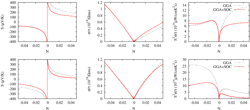
The transport coefficients calculations are performed, based on CSTA Boltzmann theory within rigid band approach. The calculated electrical conductivity depends on scattering time, while Seebeck coefficient S is independent of scattering time. By simply moving the position of Fermi level, the doping effects can be simulated. When the Fermi level is shifted into conduction (valence) bands, the n(p)-type doping is achieved with negative (positive) doping levels, giving the negative (positive) Seebeck coefficient. For monolayer MoSSe and WSSe, at room temperature, the Seebeck coefficient S, electrical conductivity with respect to scattering time and power factor with respect to scattering time as a function of doping level (N) using GGA and GGA+SOC are plotted in Figure 5, and FIG.5 and FIG.6 in the SI show ones of monolayer MoSTe, WSTe, MoSeTe and WSeTe. For MoXY, a detrimental influence on p-type S can be induced by SOC, while a neglectful effect on S (absolute value) in n-type doping can be observed. The SOC can lift the valence band degeneracy near the K point, which reduces slope of density of states (DOS) of valence bands near the energy gap, giving rise to reduced Seebeck coefficient. However, the weak SOC effects on conduction bands near the Fermi level are observed, leading to a neglectful effect on n-type S. For WXY, a reduced influence on both n- and p-type S can be observed at the presence of SOC, which can be explained by SOC-induced spin-orbit splitting of both conduction and valence bands, reducing slope of DOS near the energy gap. In n-type doping, the power factor of WXY with GGA+SOC is smaller than one using GGA. For Mo/WSSe and Mo/WSeTe, p-type power with GGA+SOC is lower than one with GGA. These can be understood by SOC effects on S and . It is noted that theses results depend on the lattice constants. When the SOC is considered, the strength of bands convergence is enhanced, and the S would be improved, producing enhanced power factor, which has been observed in TMD monolayer (X=S, Se and Te)q20 .
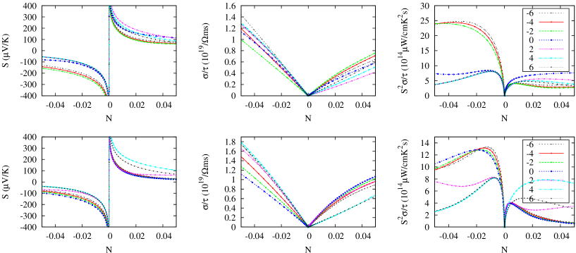
At 300 K, the biaxial strain dependence of S, and of monolayer MoSSe and WSSe are shown in Figure 6 using GGA+SOC, and FIG.7 and FIG.8 in the SI show ones of monolayer MoSTe, WSTe, MoSeTe and WSeTe. The complex strain dependence of transport coefficients are observed, which is because their energy band structures are sensitively dependent on strain. Strain-enhanced S can be understood by strain-driven accidental degeneracies, namely bands convergence. For example MoSSe, in considered n-type doping range, the largest S can be observed with -2% strain due to the near degeneracy among CBE along K-, along -M and at K point. In fact, the MoSSe with -6% and -4% strain have similar S with one with -2% due to the bands convergence of CBE along K- and -M, leading to very large n-type power factor. In p-type doping of WSSe, S reaches the largest values with 4% strain due to the energy levels of K and points being more close, leading to largest p-type power factor. It is found that the and S show usually opposite strain dependence. For MoSSe, WSSe, MoSTe and MoSeTe, strain-enhanced n-type power factor is larger than p-type one, while it is opposite for WSTe and WSeTe. An upper limit of , neglecting , can be defined as . The relates to via the Wiedemann-Franz law: , and then , where L is the Lorenz number. Therefore, the power factor is improved by enhanced S induced by strain, which is beneficial to better thermoelectric properties. Strain-improved power factor can also be observed in TMD monolayersq21 ; q21-2 ; q22 ; q23 ; qin1 .
IV Discussions and Conclusion
For TMD monolayers, the SOC produces a remarkable influence on S caused by SOC-removed the band degeneracy, and further affects the power factorq20 ; q21 ; q21-2 ; q23 . The SOC not only can reduce the power factor, but can also obviously improve one like (X=S, Se and Te)q20 . However, for unstrained MXY (M = Mo or W, X/Y = S, Se, or Te) monolayer, only obviously reduced effect can be observed by SOC. The strain-improved S can also found in TMD monolayers, such as , , , and q21 ; q21-2 ; q22 ; q23 ; qin1 , and the related mechanism is similar with that of strain-enhanced S of Janus TMD monolayers. Besides strain, electric field can also effectively tune the electronic structures of 2D materials, so it is possible to tune S of Janus TMD monolayers by electric field. The Janus TMD monolayers may have better thermoelectric properties than TMD monolayers due lower . It has been proved that the MoSSe (ZrSSe) has lower than ()p4 ; p4-1 , and the ZrSSe has enhanced n-type thermoelectric properties compared with monolayer p4-1 .
In summary, we systematically study strain dependence of electronic structures and transport coefficients of Janus MXY (M = Mo or W, X/Y = S, Se, or Te) monolayer, based mainly on the reliable first-principle calculations. Calculated results show that the inclusion of SOC is key for energy band structures of Janus TMD monolayers, which has important effects on their electronic transport coefficients. It is found that both compressive and tensile strain can tune the strength of bands convergence by changing the numbers and relative position of VBE or CBE, producing important effects on their electronic transport coefficients. For all Janus TMD monolayers, the S can be enhanced by choosing the appropriate compressive or tensile strain, and then the power factor can be improved. Our works will motivate farther experimental studies, and studies of electronic transports of other Janus TMD monolayers.
Acknowledgements.
This work is supported by the National Natural Science Foundation of China (Grant No. 11404391). We are grateful to the Advanced Analysis and Computation Center of CUMT for the award of CPU hours to accomplish this work.References
- (1) Y. Pei, X. Shi, A. LaLonde, H. Wang, L. Chen and G. J. Snyder, Nature 473, 66 (2011).
- (2) A. D. LaLonde, Y. Pei, H. Wang and G. J. Snyder, Mater. Today 14, 526 (2011).
- (3) M. S. Dresselhaus et al. Adv. Mater. 19, 1043 (2007).
- (4) L. D. Hicks and M. S. Dresselhaus, Phys. Rev. B 47, 12727 (1993).
- (5) L. D. Hicks and M. S. Dresselhaus, Phys. Rev. B 47, 16631(R) (1993).
- (6) K. S. Novoselov et al., Science 306, 666 (2004).
- (7) M. Chhowalla, H. S. Shin, G. Eda, L. J. Li, K. P. Loh and H. Zhang, Nature Chemistry 5, 263 (2013).
- (8) R. X. Fei, W. B. Li, J. Li and L. Yang, Appl. Phys. Lett. 107, 173104 (2015).
- (9) S. L. Zhang M. Q. Xie, F. Y. Li, Z. Yan, Y. F. Li, E. J. Kan, W. Liu, Z. F. Chen, H. B. Zeng, Angew. Chem. 128, 1698 (2016).
- (10) J. P. Ji, X. F. Song, J. Z. Liu et al., Nat. Commun. 7, 13352 (2016).
- (11) S. Balendhran, S. Walia, H. Nili, S. Sriram and M.Bhaskaran, small 11, 640 (2015).
- (12) W. Huang, H. X. Da and G. C. Liang, J. Appl. Phys. 113, 104304 (2013).
- (13) G. Qin, Z. Qin, W. Fang, L. Zhang, S. Yue, Q. Yan, M. Hu and G. Su, Nanoscale 8, 11306 (2016).
- (14) S. D. Guo and Y. H. Wang, J. Appl. Phys. 121, 034302 (2017).
- (15) G. P. Li, G. Q. Ding and G. Y. Gao, J. Phys.: Condens. Matter 29, 015001 (2017).
- (16) D. C. Zhang, A. X. Zhang, S. D. Guo and Y. F. Duan, RSC Adv. 7, 24537 (2017).
- (17) L. M. Sandonas,D. Teich, R. Gutierrez, T. Lorenz, A. Pecchia, G. Seifert and G. Cuniberti, J. Phys. Chem. C 120, 18841 (2016).
- (18) S. D. Guo, A. X. Zhang and H. C. Li, Nanotechnology 28, 445702 (2017).
- (19) G. P. Li, K. L. Yao and G. Y. Gao, Nanotechnology 29, 015204 (2018).
- (20) S. D. Guo and J. L. Wang, Semicond. Sci. Tech. 31, 095011 (2016).
- (21) S. D. Guo and Y. Wang, Semicond. Sci. Tech. 32, 055004 (2017).
- (22) E. Scalise, M. Houssa, G. Pourtois, V. Afanas’ev and A. Stesmans, Nano Res. 5, 43 (2012).
- (23) S. D. Guo, Comp. Mater. Sci. 123, 8 (2016).
- (24) H. Y. Lv, W. J. Lu, D. F. Shao, H. Y. Lub and Y. P. Sun, J. Mater. Chem. C 4, 4538 (2016).
- (25) S. D. Guo, J. Mater. Chem. C 4, 9366 (2016).
- (26) A. Y. Lu, H. Y. Zhu, J. Xiao et al., Nature Nanotechnology 12, 744 (2017).
- (27) X. C. Ma, X. Wu, H. D. Wang and Y. C. Wang, J. Mater. Chem. A 6, 2295 (2018).
- (28) L. Dong, J. Lou and V. B. Shenoy, ACS Nano 11, 8242 (2017).
- (29) W. J. Yin, B. Wen, G. Z. Nie and X. L. Wei and L. M. Liu, J. Mater. Chem. C 6 1693 (2018).
- (30) F. P. Li, W. Wei, P. Zhao, B. B. Huang and Y. Dai, J. Phys. Chem. Lett. 8, 5959 (2017).
- (31) S. D. Guo, Phys. Chem. Chem. Phys. 20, 7236 (2018).
- (32) S. D. Guo, arXiv:1712.09064 (2017).
- (33) P. Hohenberg and W. Kohn, Phys. Rev. 136, B864 (1964); W. Kohn and L. J. Sham, Phys. Rev. 140, A1133 (1965).
- (34) P. Blaha, K. Schwarz, G. K. H. Madsen, D. Kvasnicka and J. Luitz, WIEN2k, an Augmented Plane Wave + Local Orbitals Program for Calculating Crystal Properties (Karlheinz Schwarz Technische Universität Wien, Austria) 2001, ISBN 3-9501031-1-2
- (35) J. P. Perdew, K. Burke and M. Ernzerhof, Phys. Rev. Lett. 77, 3865 (1996).
- (36) A. H. MacDonald, W. E. Pickett and D. D. Koelling, J. Phys. C 13, 2675 (1980).
- (37) D. J. Singh and L. Nordstrom, Plane Waves, Pseudopotentials and the LAPW Method, 2nd Edition (Springer, New York, 2006).
- (38) J. Kunes, P. Novak, R. Schmid, P. Blaha and K. Schwarz, Phys. Rev. B 64, 153102 (2001).
- (39) D. D. Koelling, B. N. Harmon, J. Phys. C: Solid State Phys. 10, 3107 (1977).
- (40) G. K. H. Madsen and D. J. Singh, Comput. Phys. Commun. 175, 67 (2006).
- (41) X. F. Wu, V. Varshney et al., Chem. Phys. Lett. 669, 233 (2017).
- (42) D. Qin, X. J. Ge, G. Q. Ding, G. Y. Gao and J. T. Lv, RSC Adv. 7, 47243 (2017).