Double inverse nanotapers for efficient light coupling to integrated photonic devices
Abstract
Efficient light coupling into integrated photonic devices is of key importance to a wide variety of applications. "Inverse nanotapers" are widely used, in which the waveguide width is reduced to match an incident mode. Here, we demonstrate novel, "double inverse" tapers, in which we taper both the waveguide height, as well as the width. We demonstrate that in comparison to regular inverse tapers, the double inverse tapers have excellent polarization-independent coupling. In addition, the optimum coupling is achieved with much larger taper dimension, enabling the use of photolithography instead of electron beam lithography, relevant for applications at near-IR and visible wavelengths. The low coupling loss makes them particularly suitable for nonlinear photonics, e.g. supercontinuum and soliton micro-comb generation.
Photonic integrated circuits (PIC) allow for manipulation of light on chip-scale devices and have evolved into a mature technology ("silicon photonics"). Over the past decades, a broad range of applications based on PIC, passive or active, have been demonstrated such as filters Little et al. (1997), modulators Reed et al. (2010) and lasers (Liang and Bowers, 2010), that are now employed in data-centers. A second wave of interest in integrated photonic devices such as waveguides and resonators, has recently emerged with the advances in their use for nonlinear frequency conversion Foster et al. (2006); Moss et al. (2013). On the one hand, the tight waveguide confinement allows significantly higher effective nonlinearity than that of optical fibers, when combined with materials such as silicon (Si), Si3N4 and AlGaAs that exhibit high material nonlinearity. On the other hand, integrated waveguides enable the engineering of dispersion properties Foster et al. (2006), in particular the anomalous group velocity dispersion (GVD), a prerequisite for parametric frequency conversion and soliton formation. These advances, along with the fabrication of low loss optical microresonators, have enabled in particular Kerr soliton frequency comb generation in integrated optical microresonators with engineered GVD Kippenberg et al. (2011), as well as broadband spectra using higher order dispersion engineering via soliton induced Cherenkov radiation Brasch et al. (2016); Pfeiffer et al. (2017); Li et al. (2017). Moreover, waveguides of engineered dispersion have enabled supercontinuum generation at low pulse energies, i.e. octave spanning combs with pJ pulse energy Herkommer et al. (2017). These advances signal the potential of integrated nonlinear photonic devices, that have applications such as low noise microwave Liang et al. (2015), coherent communication Marin-Palomo et al. (2017), spectroscopy Yu et al. (2016); Suh et al. (2016), astronomical spectrometer Obrzud et al. (2017); Suh et al. (2018) and LIDAR Trocha et al. (2017); Suh and Vahala (2017).
Central to nonlinear photonic applications is the ability to couple light to photonic chip devices with low loss over a broad optical bandwidth. Widely employed grating couplers Taillaert et al. (2006) are not well suited for this purpose due to their restricted bandwidth. In contrast, inverse nanotapers (Almeida et al., 2003), possessing simultaneously high coupling efficiency, broad operation bandwidth and the use of standard CMOS-compatible fabrication process, are widely used in PIC based chip devices and particularly well suited for nonlinear integrated photonics. An inverse taper works as a mode transformer which adiabatically transforms an incident fiber or free-space optical mode (of several micron mode diameter) to a waveguide mode (of sub-micron mode diameter). The taper mode at the device facet matches the incident fiber or free-space mode, due to the small taper waveguide size and thus the strong evanescent field.
In this Letter, we present novel, double inverse tapers ("2D-tapers") for efficient light coupling from lensed fibers to Si3N4 waveguides. In comparison with the regular inverse tapers ("1D-tapers") which have only the reduced waveguide width to match the incident mode (as shown in Fig. 1(a)), 2D-tapers have both the reduced waveguide height as well as the width (as shown in Fig. 2(b)). First, we present the simulation of light coupling from a lensed fiber to Si3N4 bus waveguides via 1D-tapers, using 3D finite-difference time-domain (FDTD) simulation. We fabricate 1D-tapers of 820 nm height but different widths, experimentally characterize their coupling efficiencies at 1550 nm wavelength, and demonstrate that >45 coupling efficiency for the transverse electric (TE) polarization can only be achieved in a taper of 80 nm width. Such small feature can only be achieved with electron beam lithography (EBL). We also reveal that the coupling efficiency for the transverse magnetic (TM) polarization is lower than the TE polarization due to the taper’s large height-to-width aspect ratio (HWAR). To relax the stringent lithography requirement to fabricate tapers of 80 nm width and to further improve the coupling for the TM polarization, we fabricate 2D-tapers using the novel photonic Damascene process (Pfeiffer et al., 2016). Due to the inherent aspect-ratio-dependent etch (ARDE), the 2D-tapers have increasing height over taper length, therefore enabling further reduction of the taper size. We demonstrate >45 coupling efficiency at 1550 nm wavelength, for both the TE and TM polarizations in 2D-tapers of >300 nm width, which can be easily achieved with deep-UV lithography, significantly relaxing the lithography requirement. Furthermore, by comparing the coupling performance of several groups of 2D-tapers, we demonstrate the flexibility to engineer the 2D-taper’s shape, enabling >45 coupling efficiency with 500 nm taper width. Therefore these 2D-tapers are promising for light coupling at short wavelength range e.g. 1064 nm or 780 nm, which is usually challenging as EBL is required to pattern very small taper size for optimized coupling.
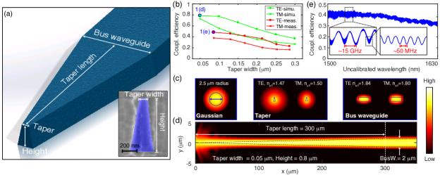
We experimentally study Si3N4 waveguides fully buried in SiO2 cladding, as shown in Fig. 1(a). The 1D-tapers are fabricated using a subtractive process Gondarenko et al. (2009), a standard CMOS-compatible fabrication process widely used for integrated photonic devices. In our process, patterns e.g. tapers and bus waveguides, are defined by EBL and transferred to Si3N4 film via dry etching (CHF3/O2). All the patterns, including tapers and bus waveguides, have the uniform height as the Si3N4 film thickness. As shown in Fig. 1(a), tapers fabricated using this process have increasing width but constant height over the taper length.
We simulate the light coupling from a lensed fiber to Si3N4 bus waveguides via 1D-tapers of different taper widths at a chip facet, using FDTD method. Due to the Si3N4 dry etching process, the 1D-tapers as well as the bus waveguides have a sidewall bottom angle of 80o. In this Letter, the "taper width" is defined as the top side width of the taper’s trapezoidal cross-section (see Fig. 1(a) inset), which is defined by EBL. Other taper parameters used in the simulation are shown in Fig. 1(c), (d). We use a free-space Gaussian mode of 2.5 m waist diameter to represent the incident mode from the lensed fiber, according to the lensed fiber’s specification. The normalized transmitted power through the bus waveguide, i.e. coupling efficiency per chip facet , can be calculated in the simulation. Thus the full device coupling efficiency including two facets is defined as .
We simulate at the wavelength 1550 nm, for both the TE and TM polarizations of the incident Gaussian mode. The simulated as function of taper width from 50 to 300 nm is shown in Fig. 1(b), together with the experimentally measured data which, will be discussed later.
The simulation results present two prominent trends: First, a smaller taper has better coupling, due to the weaker light confinement (lower effective refractive index) which improves the mode match to the incident Gaussian mode. Second, the TE mode has better coupling than the TM mode. As shown in Fig. 1(c), due to the taper’s high height-to-width aspect ratio (HWAR), the TE mode has a larger size than the TM mode, leading to a better match to the incident Gaussian mode. Fig. 1(d) show the simulated mode propagation profile of the case of 80 coupling efficiency, illustrating that a small taper providing improved mode match can well guide the incident Gaussian mode to the bus waveguide.
We fabricate a large number of 1D-taper chips of 820 nm bus waveguide height (as the Si3N4 film thickness), and experimentally characterize their coupling efficiencies at 1550 nm wavelength, using a setup similar to the one described in Ref. Pfeiffer et al. (2017). The measured coupling efficiency of each sample, plotted in Fig. 1(b), agrees well with the simulated results, supporting the two aforementioned claims: A smaller taper has better coupling, and the TE mode has better coupling than the TM mode. The deviation between the measured data and the simulated results is likely due to the fact that the lensed fiber we use has non-unity transmission. We also characterize the coupling from 1500 to 1630 nm bandwidth, using a tunable laser. A weak trend of decreasing coupling efficiency with increasing wavelength is observed, as shown in Fig. 1(e). However this trend is more likely caused by the broadband response of e.g. the 50-50 fiber couplers used in the setup rather than the taper itself, as the opposite trend, increasing coupling efficiency with increasing wavelength, is observed when the 50-50 fiber coupler’s two output branches are interchanged. Nevertheless, the coupling efficiency remains >30 over the 130 nm range.
As mentioned above, 1D-tapers show polarization-dependent coupling, i.e. the TM polarization has lower coupling efficiency than the TE polarization, due to the 1D-taper’s large HWAR. However, many photonic devices are specifically operated with TM mode, to couple vertically between different components, such as the coupling between photonic dielectric and plasmonic waveguides Christ et al. (2003); Briggs et al. (2010). Therefore for these devices, efficient TM coupling is important and needs to be optimized.
Further improving the TM coupling requires reducing the taper size. However reducing the taper width further is challenging due to the lithography resolution and quality. In addition, thin but tall tapers of high HWAR tend to collapse which reduces fabrication yield. Therefore, reducing the taper height is a feasible solution, however simultaneously the height of other components, e.g. bus waveguides, should remain unchanged in order to operate the device in the same situation. As a result, tapers of both increasing width and height, manifesting as "double inverse tapers" or "2D-tapers", are desired.
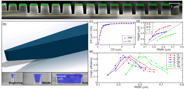
In the subtractive process all the patterns have the uniform height determined by the Si3N4 film thickness, thus 2D-tapers can not be achieved. Therefore, we use the photonic Damascene proess (Pfeiffer et al., 2016). In this process, the patterns are defined by lithography and then transferred to a SiO2 substrate via dry etching. The Si3N4 film is then deposited on the SiO2 substrate and fill the defined pattern trenches, followed by a chemical mechanical planarization (CMP) which removes the excess Si3N4 and planarizes the wafer top surface. As the dry etching process has inherently aspect-ratio-dependent etch (ARDE) rate Gottscho (1992), the pattern trench depth increases with increasing pattern size. For pattern sizes exceeding a certain threshold value, the ARDE effect becomes negligible, thus the trench depths can be considered as uniform. As a consequence, a taper of increasing width has increasing height, manifesting a 2D-taper. Other components, e.g. bus waveguides, have uniform height on the wafer.
| Chips | 1D | 2D-A | 2D-B | 2D-C |
|---|---|---|---|---|
| Mask thickness (nm) | 400 | 400 | 750 | |
| Bus waveguide height (nm) | 820 | 820 | 650 | 670 |
Fig. 2(a) shows the ARDE effect on a SiO2 substrate, after SiO2 dry etching process (C4F8/He) with a 400 nm amorphous Si etch mask. The ARDE effect creates non-uniform, pattern-dependent trench depths, and is characterized by measuring the mean etch rate (ER) as function of trench width (critical dimension, CD), as shown in Fig. 2(c). When CD reaches the threshold value of 1 m, the ER reaches a stable value of 0.29 m/min and becomes nearly independent of CD. From 0 to 0.5 m CD, ER increases nearly linearly. The ARDE curve can be fitted with , with m/min, m, m/min. Fig. 2(b) shows the measured SEM images of taper cross-sections at taper beginning (chip facet side), middle, and end (bus waveguide side), revealing the double inverse shape with increasing width and height of the waveguide.
Three groups of 2D-taper chips (Chips 2D-A, B, C) were fabricated and their specifications are shown in Tab. 1, in comparison with the 1D-taper chip. These tapers’ HWARs and coupling efficiencies for both the TE and TM polarizations are experimentally characterized, as shown in Fig. 2(d) and (e). Again, the taper width is defined as the taper’s top side width. Compared with the 1D-taper chip shown in Fig.1(b), Chip 2D-A achieves >45 TM coupling, while >45 TE coupling is maintained. Different from the 1D-tapers in which the smaller taper width shows better coupling, in Chip 2D-A, there is an optimum coupling point which is achieved with >300 nm taper width, due to the ARDE and the reverse trapezoidal shape (bottom angle 96o). This optimum coupling requires weak waveguide confinement for large taper mode of improved mode match, but simultaneously the waveguide confinement needs to be sufficient to overcome the Gaussian beam’s divergence. Such >300 nm taper width of optimum coupling can be easily achieved with deep-UV lithography instead of EBL, significantly relaxing the stringent requirement of lithography resolution. Moreover, optimized coupling for shorter wavelengths, e.g. 1064 nm and 780 nm, requires very small tapers, which is challenging to fabricate with 1D-tapers due to the waveguide height. Therefore 2D-tapers are more useful to work in these wavelengths.
The ARDE and the taper shape can be engineered simply by changing the etch mask thickness. A thicker etch mask gives a stronger ARDE effect. To demonstrate this scheme, 2D-taper Chips, 2D-B and 2D-C, are fabricated. Chip 2D-C is fabricated with a 750 nm deep-UV photoresist etch mask, leading to a stronger ARDE. Chip 2D-B is fabricated with a 400 nm amorphous Si etch mask, same process as Chip 2D-A but the bus waveguide height is made to 650 nm via more CMP time, in order to directly compare to Chip 2D-C. Both chips have nearly the same bus waveguide height (66010 nm), but their taper HWARs are significantly different due to their different ARDEs, as shown in Fig. 2(d). As shown in Fig. 2(e), compared with Chip 2D-A, the coupling of Chip 2D-B is not prominently different, because, as long as the taper’s HWAR exceeds unity (>1), the mode size is more constrained by the taper width rather than the taper height. However, the stronger ARDE (HWAR <1) of Chip 2D-C shifts the optimum coupling to taper width >500 nm. In this case the required lithography precision is further reduced, enabling the use of common UV lithography.
In summary, we present the characterization of inverse (1D-) and double inverse (2D-) tapers for efficient light coupling from a lensed fiber to Si3N4 waveguides. We experimentally compare the coupling performance of 1D- and 2D-tapers, and illustrate the main mechanisms in the fabrication processes which lead to the performance difference. We demonstrate the advantages of 2D-tapers, including: First, better coupling of the TM polarization. Second, larger taper width at optimum coupling, enabling the use of UV or deep-UV photolithography instead of EBL. Third, flexibility to change the taper shapes via engineering the ARDE effect. The data presented in this Letter is from several chip devices, but is highly reproduceable in many other chips that we have experimentally characterized. Our results demonstrate the advantages of 2D-tapers over 1D-tapers, particularly promising for light coupling at near-IR or visible wavelengths.
Funding Information
Defense Advanced Research Projects Agency (DARPA), Defense Sciences Office (DSO) (HR0011-15-C-0055); European Union’s Horizon 2020 Framework Programme (H2020) (709249); Swiss National Science Foundation (SNSF) (161573).
Acknowledgements
We thank Tiago Morias in assisting the sample fabrication. The Si3N4 optical waveguide samples were fabricated in the EPFL center of MicroNanoTechnology (CMi).
References
- Little et al. (1997) B. E. Little, S. T. Chu, H. A. Haus, J. Foresi, and J. Laine, Journal of Lightwave Technology 15, 998 (1997).
- Reed et al. (2010) G. T. Reed, G. Mashanovich, F. Y. Gardes, and D. J. Thomson, Nature Photonics 4, 518 (2010).
- Liang and Bowers (2010) D. Liang and J. E. Bowers, Nature Photonics 4, 511 (2010).
- Foster et al. (2006) M. A. Foster, A. C. Turner, J. E. Sharping, B. S. Schmidt, M. Lipson, and A. L. Gaeta, Nature 441, 960 (2006).
- Moss et al. (2013) D. J. Moss, R. Morandotti, A. L. Gaeta, and M. Lipson, Nature Photonics 7, 597 (2013).
- Kippenberg et al. (2011) T. J. Kippenberg, R. Holzwarth, and S. A. Diddams, Science 332, 555 (2011).
- Brasch et al. (2016) V. Brasch, M. Geiselmann, T. Herr, G. Lihachev, M. H. P. Pfeiffer, M. L. Gorodetsky, and T. J. Kippenberg, Science 351, 357 (2016).
- Pfeiffer et al. (2017) M. H. P. Pfeiffer, C. Herkommer, J. Liu, H. Guo, M. Karpov, E. Lucas, M. Zervas, and T. J. Kippenberg, Optica 4, 684 (2017).
- Li et al. (2017) Q. Li, T. C. Briles, D. A. Westly, T. E. Drake, J. R. Stone, B. R. Ilic, S. A. Diddams, S. B. Papp, and K. Srinivasan, Optica 4, 193 (2017).
- Herkommer et al. (2017) C. Herkommer, A. Billat, H. Guo, D. Grassani, C. Zhang, M. H. P. Pfeiffer, C.-S. Bres, and T. J. Kippenberg, arXiv 1704.02478v2 (2017).
- Liang et al. (2015) W. Liang, D. Eliyahu, V. S. Ilchenko, A. A. Savchenkov, A. B. Matsko, D. Seidel, and L. Maleki, Nature Communications 6, 7957 (2015).
- Marin-Palomo et al. (2017) P. Marin-Palomo, J. N. Kemal, M. Karpov, A. Kordts, J. Pfeifle, M. H. P. Pfeiffer, P. Trocha, S. Wolf, V. Brasch, M. H. Anderson, R. Rosenberger, K. Vijayan, W. Freude, T. J. Kippenberg, and C. Koos, Nature 546, 274 (2017).
- Yu et al. (2016) M. Yu, Y. Okawachi, A. G. Griffith, N. Picqué, M. Lipson, and A. L. Gaeta, arXiv 1610.01121v2 (2016).
- Suh et al. (2016) M.-G. Suh, Q.-F. Yang, K. Y. Yang, X. Yi, and K. J. Vahala, Science 354, 600 (2016).
- Obrzud et al. (2017) E. Obrzud, M. Rainer, A. Harutyunyan, M. H. Anderson, M. Geiselmann, B. Chazelas, S. Kundermann, S. Lecomte, M. Cecconi, A. Ghedina, E. Molinari, F. Pepe, F. Wildi, F. Bouchy, T. J. Kippenberg, and T. Herr, arXiv 1712.09526 (2017).
- Suh et al. (2018) M.-G. Suh, X. Yi, Y.-H. Lai, S. Leifer, I. S. Grudinin, G. Vasisht, E. C. Martin, M. P. Fitzgerald, G. Doppmann, J. Wang, D. Mawet, S. B. Papp, S. A. Diddams, C. Beichman, and K. Vahala, arXiv 1801.05174 (2018).
- Trocha et al. (2017) P. Trocha, D. Ganin, M. Karpov, M. H. P. Pfeiffer, A. Kordts, J. Krockenberger, S. Wolf, P. Marin-Palomo, C. Weimann, S. Randel, W. Freude, T. J. Kippenberg, and C. Koos, arXiv 1707.05969v2 (2017).
- Suh and Vahala (2017) M.-G. Suh and K. Vahala, arXiv 1705.06697v3 (2017).
- Taillaert et al. (2006) D. Taillaert, F. Van Laere, M. Ayre, W. Bogaerts, D. Van Thourhout, P. Bienstman, and R. Baets, Japanese Journal of Applied Physics, Part 1: Regular Papers and Short Notes and Review Papers 45, 6071 (2006).
- Almeida et al. (2003) V. R. Almeida, R. R. Panepucci, and M. Lipson, Optics Letters 28, 1302 (2003).
- Pfeiffer et al. (2016) M. H. P. Pfeiffer, A. Kordts, V. Brasch, M. Zervas, M. Geiselmann, J. D. Jost, and T. J. Kippenberg, Optica 3, 20 (2016).
- Gondarenko et al. (2009) A. Gondarenko, J. S. Levy, and M. Lipson, Optics Express 17, 11366 (2009).
- Christ et al. (2003) A. Christ, S. G. Tikhodeev, N. A. Gippius, J. Kuhl, and H. Giessen, Physical Review Letters 91, 183901 (2003).
- Briggs et al. (2010) R. M. Briggs, J. Grandidier, S. P. Burgos, E. Feigenbaum, and H. A. Atwater, Nano Letters 10, 4851 (2010).
- Gottscho (1992) R. A. Gottscho, Journal of Vacuum Science & Technology B: Microelectronics and Nanometer Structures 10, 2133 (1992).