Tunability of electronic and optical properties of the Ba-Zr-S system via dimensional reduction
Abstract
Transition metal sulfide perovskites offer lower band gaps and greater tunability than oxides, along with other desirable properties for applications. Here we explore dimensional reduction as a tuning strategy using the Ruddlesden-Popper phases in the Ba-Zr-S system as a model. The three dimensional perovskite BaZrS3 is a direct gap semiconductor, with a band gap of 1.5 eV suitable for solar photovoltaic application. However, the three known members of the Ruddlesden-Popper series, are all indirect gap materials, and additionally have lower fundamental band gaps. This is accompanied in the case of Ba2ZrS4 by a band structure that is more favorable for carrier transport for oriented samples. The layered Ruddlesden-Popper compounds show significantly anisotropic optical properties, as may be expected. The optical spectra show tails at low energy, which may complicate experimental characterization of these materials.
I Introduction
The sulfide perovskite BaZrS3 has a moderate band gap of less than 2 eV and exhibits ambipolar doping. Perera et al. (2016); Niu et al. (2017); Sun et al. (2015); Meng et al. (2016) This is in contrast to the corresponding oxide, BaZrO3 (band gap 5.3 eV). Robertson (2000) Furthermore, there is evidence that the band gap of BaZrS3 might be considerably tuned by substitutions on the normally inactive -site of the perovskite structure, Niu et al. (2017, 2018) also different from most semiconducting perovskite oxides. Tunability of electronic and optical properties is an important consideration for electronic and optoelectronic applications. This is exemplified by the wide tunability in III-V and II-VI zinc blende structure semiconductor alloys. These alloys thus have a multitude of ensuing applications and are the basis of key technologies. In fact, it is known that the properties of sulfide perovskites can be modified by alloying, for example with Ti, but the lack of stability of the Ba(Zr,Ti)S3 alloy is a challenge. Meng et al. (2016) In addition to transition metal alloying, substitutions for Ba on the perovskite -site, and chalcogen alloys are also possible and may be effective in tuning the electronic and optical properties. However, alternatives are desirable.
Dimensional reduction is another highly effective general method for modifying electronic structures of semiconductors. This can be done by artificial methods, such as through quantum wells and superlattices, which are important for semiconductor technologies. Kroemer (1963) Additionally, the electronic structure changes associated with dimensional reduction may be important for a wide variety of applications, including for example, thermoelectrics, where they can decouple the thermopower and conductivity, Hicks and Dresselhaus (1993); Zhang et al. (2016); Xing et al. (2017); Terasaki et al. (1997) optoelectronic materials, such as transparent conductors, Li et al. (2015) and a wide variety of optical, electronic and other applications based on 2D materials. Wang et al. (2012); Butler et al. (2013)
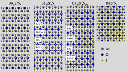
Dimensional reduction in the electronic structure of materials can be achieved in various ways. These include artificial structures, such as superlattices, exfoliation or thin film growth to produce 2D materials, interfacial electron gasses, Ohtomo and Hwang (2004) bonding structures that lower the effective dimensionality, Parker et al. (2013) and the production of homologous series of layered compounds, such as the Ruddlesden-Popper (RP) series for perovskites. Ruddlesden and Popper (1957) This series consists of perovskite structure blocks separated by extra rock salt layers along a [001] direction. The first element of this series is the K2NiF4 structure, which is the prototype structure of the high temperature superconductors.
In the case of BaZrS3 three members of the RP series, Ban+1ZrnS3n+1, where is the number of layers in the perovskite block, are known experimentally. Lelieveld and Ijdo (1980); Saeki et al. (1991); Chen et al. (1994, 1993) These are the =1, 2 and 3 members, Ba2ZrS4, Ba3Zr2S7 and Ba4Zr3S10, in addition to the = perovskite, BaZrS3. The 3D perovskite, BaZrS3 and the =3 compound, Ba4Zr3S10 show significant distortions from the ideal structure due to rotation of the ZrS6 octahedra, consistent with the fact that the perovskite tolerance factor, =0.95 (based on Shannon crystal radii)Shannon (1976) is smaller than unity for these compounds, while the =1 and =2 compounds have been reported to occur in an ideal undistorted body centered tetragonal structure.
The purpose of this paper is to report a consistent set of first principles electronic structures and optical properties for this series of compounds. We find that dimensional reduction lowers the band gap in contrast to most oxide perovskites, and that additionally it changes the band gap character from direct in the 3D perovskite to indirect in the layered RP compounds. We also find that dimensional reduction can substantially enhance carrier transport for both electrons and holes in suitably oriented samples.
II Structure and Methods
Our calculations were done within density functional theory (DFT). The electronic structures and optical properties were calculated using the general potential linearized augmented planewave (LAPW) method, Singh and Nordstrom (2006) as implemented in the WIEN2k code. Blaha et al. (2001) The total energy calculations and relaxation of the atomic coordinates were done using the PBE generalized gradient approximation. Perdew et al. (1996) For these relaxations, relativity was treated at a scalar relativistic level, and relaxation was continued until all force components were below 1 mRy/Bohr (0.025 eV/Å). LAPW sphere radii of 2.5 bohr, for Ba, 2.3 Bohr for S and 2.3 Bohr, for Zr were used, except for Ba2ZrS4, for which the S radius was reduced to 2.2 Bohr to accommodate the shorter bond length in this compound. The basis sets were defined by a planewave sector basis cutoff determined by =9, where is the smallest LAPW sphere radius. The standard LAPW augmentation was employed. Local orbitals were added to the basis to treat semicore states. We used the experimental lattice parameters from literature, and relaxed all internal atomic coordinates by total energy minimization. Specifically, we used space group , =7.0599 Å, =9.9813 Å, =7.0251 Å, for BaZrS3, Lelieveld and Ijdo (1980) space group , =4.7852 Å, =15.9641 Å, for Ba2ZrS4, Saeki et al. (1991) space group , =4.9983 Å, =25.502 Å, for Ba3Zr2S7, Chen et al. (1994) and space group , =7.0314 Å, =7.0552 Å, =35.544 Å, for Ba4Zr3S10. Chen et al. (1993) In the case of Ba3Zr2S7, we also performed calculations for the orthorhombic structure reported by Saeki, Saeki et al. (1991) but find that it is not energetically favored. The crystal structures are depicted in Fig. 1. The relaxed atomic coordinates are given in Tab. 1.
Spin-orbit was included for the electronic and optical properties. The band gap is important for these, and accordingly these calculations were done using the modified Becke-Johnson potential of Tran and Blaha. Tran and Blaha (2009) This functional gives band gaps in good accord with experiment for a wide variety of simple semiconductors and insulators. Tran and Blaha (2009); Koller et al. (2011); Singh (2010) Calculation of the transport function for conductivity was done using the BoltzTraP code. Madsen and Singh (2006) Optical properties were calculated based on electric dipole transitions in the independent particle approximation as implemented in the WIEN2k code.
III Results and Discussion
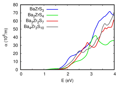
We begin with our electronic structure results. The electronic densities of states (DOS) of the different compounds are compared in Fig. 2, and the calculated direction averaged optical absorption spectra are compared in Fig. 3. The band gaps and onsets of optical absorption are listed in Table 2. Rock salt structure BaS has an indirect band gap of 3.32 eV based on the same method. Thus we find BaS to be a wide band gap material, consistent with other reports. Zagorac et al. (2017) The implication of the wide gap of BaS is that the rock salt parts of the unit cells of the RP phases can be expected to serve as blocking layers from an electronic point of view, so that the RP phases may be expected to show 2D characteristics in their electronic structure.
| BaZrS3 | |||
| =7.0599 Å, | =9.9813 Å, | =7.0251 Å | |
| Ba | 0.4495 | 1/4 | 0.0098 |
| Zr | 0 | 0 | 0 |
| S1 | 0.5040 | 1/4 | 0.5673 |
| S2 | 0.2084 | 0.0348 | 0.2913 |
| Ba2ZrS4 | |||
| =4.7852 Å, | =15.9641 Å | ||
| Ba | 0 | 0 | 0.3560 |
| Zr | 0 | 0 | 0 |
| S1 | 0 | 1/2 | 0 |
| S2 | 0 | 0 | 0.1640 |
| Ba3Zr2S7 | |||
| =4.9983 Å, | =25.502 Å | ||
| Ba1 | 0 | 0 | 1/2 |
| Ba2 | 0 | 0 | 0.3193 |
| Zr | 0 | 0 | 0.1007 |
| S1 | 0 | 1/2 | 0.0960 |
| S2 | 0 | 0 | 0.1993 |
| S3 | 0 | 0 | 0 |
| Ba4Zr3S10 | |||
| =7.0314 Å, | =7.0552 Å, | =35.544 Å | |
| Ba1 | 0 | 0 | 0.4322 |
| Ba2 | 0 | 0 | 0.3001 |
| Zr1 | 0 | 0 | 0 |
| Zr2 | 0 | 0 | 0.1436 |
| S1 | 0 | 0 | 0.0708 |
| S2 | 0 | 0 | 0.2140 |
| S3 | 1/4 | 1/4 | 0 |
| S4 | 1/4 | 1/4 | 0.1395 |
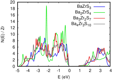
The DOS shows that the RP phases all have smaller band gaps than the 3D perovskite. This is an important consideration for solar absorber applications, discussed further below. The onset of the DOS at the top of the valence bands is similar for all the compounds in that the DOS rises sharply as the energy is lowered into the valence bands. The DOS shapes for the conduction bands of the RP phases show some qualitative characteristics expected for a 2D material, in particular, step like features as a function of energy. It is also notable that the RP phases all show a low density of states tail extending from the conduction band edge to an onset of much more steeply increasing DOS at higher energy.
BaZrS3 has been discussed as a potential solar photovoltaic material. Sun et al. (2015) BaZrS3 has a 1.50 eV direct band gap at . The other compounds are indirect band gap materials, whose indirect and optical gaps are given in Table 2. The present value for the band gap of BaZrS3 is slightly lower than our previously reported value of 1.55 eV, Niu et al. (2017) due to the inclusion of spin-orbit in the present calculation. Our value is also smaller than reported hybrid functional values of 1.7 eV – 1.8 eV, without spin orbit. Sun et al. (2015); Meng et al. (2016); Polfus et al. (2015) Experimental band gap values are limited to powder photoluminescence and diffuse reflectance measurements with Kubelka-Munk modeling. The values obtained in this way are 1.85 eV, Meng et al. (2016) 1.7 eV, Perera et al. (2016) and 1.83 eV. Niu et al. (2017) Our calculated direction dependent absorption spectra are given in Fig. 4. It will be of interest to compare with single crystal optical spectra, if suitable samples become available.
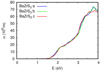
Although BaZrS3 is orthorhombic, the absorption is rather isotropic over the whole energy range, which should simplify the analysis of experimental data. The absorption onset is at the direct band gap of 1.5 eV. However, as may be seen there is a shoulder in the absorption spectrum at 2.2 eV, and at energies below this shoulder the spectrum is concave upwards, especially below 2 eV. Ordinary parabolic band direct gap semiconductors have absorption, =, where a coefficient. This form is concave downwards. The band structure is shown in Fig. 5. The unusual shape of the absorption edge is a consequence of the non-parabolicity of the bands. This is due to the near degeneracy of the bands at the -point valence and conduction band edges, as well as the related characteristic flat lowest conduction band (seen along -U) which arises from the shape of the orbitals in relation to the ligand coordination in a perovskite structure, as has been discussed elsewhere in relation to transport and optical properties of other materials. Sun and Singh (2016) In any case, this unusual shape of the optical absorption may then explain fits of optical spectra extrapolating to gap values near 1.8 eV, with the lower energy part of the spectrum perhaps mis-characterized as an Urbach tail. It will be of interest to perform quantitative analysis using single crystal absorption or reflection data should suitable samples become available.
| Compound | (ind.) (eV) | (opt.) (eV) |
|---|---|---|
| BaZrS3 | 1.50 | 1.50 |
| Ba2ZrS4 | 0.92 | 1.05 |
| Ba3Zr2S7 | 0.95 | 1.26 |
| Ba4Zr3S10 | 0.88 | 1.20 |

From the point of view of materials for photovoltaic application, the Shockley-Queisser maximum single junction efficiency curve Shockley and Queisser (1961) is essentially flat at the maximum value from 1 eV – 1.5 eV. Thus these materials all have suitable band gaps for solar applications. However, except for BaZrS3, the band gaps are indirect, which is generally unfavorable for this application. The differences between the direct and indirect band gap range from 0.13 eV in Ba2ZrS4 to 0.3 eV for the other two RP phases. The relatively smaller difference between the indirect and optical band gaps for Ba2ZrS4 and its suitable gap value mean that this materials may be the most likely of the RP phases to be a useful solar absorber, with the Ba3Zr2S7 phase next.

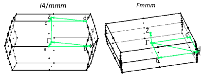
The band structure of Ba2ZrS4 is shown in Fig. 6. The path through the zone is shown in Fig. 7, and is chosen to have lines either in the basal plane (constant ) or perpendicular to it. This is in order to more clearly show the relative dispersions in-plane and out-of-plane. The lowest conduction band is very flat along -Z, meaning that it is a very 2D band. In contrast, it is very dispersive in-plane. This band is single degenerate, neglecting spin, and comes from the xy orbital of the Zr manifold. It should be noted that this orbital points in the layer plane of the K2NiF4 structure, consistent with the very weak dispersion of this band. The next conduction band at is two-fold degenerate, corresponding to the xy/xz orbitals. This band is seen to be more dispersive along (-Z), reflecting the fact that the lobes of the underlying orbitals do not point in-plane. These bands are also less dispersive than the lowest band. This lower dispersion corresponds to the smaller band width. This smaller band width explains why the band minimum for these two bands lies higher in energy than the bottom of the xy-band. This smaller width is simply understood if one considers the xy orbital, which points in-plane and so has hopping in both the x and y directions, in relation to e.g. the xz orbital, which does not have as much hopping in the y direction.
The DOS of an ideal 2D parabolic band is in the shape of a step function, with height inversely proportional to the effective mass. This is the explanation of the low value DOS tail at the conduction band edge. The top valence band is more dispersive along -Z, as are bands further from the band edges.

The band structure of the =2 compound, Ba3Zr2S7 (Fig. 8), which also occurs in an ideal tetragonal structure without octahedral rotation, can be understood in the same way. In particular, there are now two slightly split bands at the bottom of the conduction band at . These are associated with the xy orbitals of the two layers in the structure, and are weakly split because of the in-plane nature of the xy orbital. The four xz/yz bands interact more strongly and are accordingly much more strongly split at , in addition to showing stronger dispersion. In any case, the xy bands form the conduction band minimum similar to the =1 compound, and again there is a low flat tail on the DOS at the bottom of the conduction band. The =3 compound, Ba4Zr3S10 has a lower symmetry distorted orthorhombic crystal crystal structure. This leads to a more complex band structure, as shown in Fig. 9. However, the qualitative features of an indirect band gap, with a valence band maximum at the zone corner, a conduction band minimum at the zone center, and a conduction band minimum derived from bands with low dispersion along the direction remain.

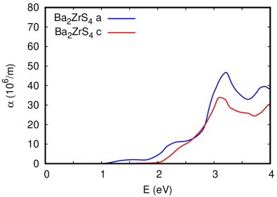
Importantly, in both the =1 and =2 compounds the valence band maximum is at the zone corner X point, while the conduction band minimum is at , as discussed above. The optical gap is at the point. This makes the low tail in the DOS also of relevance for the optical absorption spectra, shown in Figs. 10 and 11 for Ba2ZrS4 and Ba3Zr2S7, respectively. As may be seen, these features of the band structure are reflected in what might be termed a polarization dependent optical gap. What is meant by this is that the xy nature of the conduction band minimum allows optical transitions at for in-plane light polarization, but not for c-axis polarized light. For example, in Ba2ZrS4 we find that the absorption spectrum for c-axis polarized light goes smoothly to zero with an apparent optical band bap of 2 eV. On the other hand, for in-plane polarization the absorption extends to the optical gap of 1.05 eV. It is also important to note that the absorption in this foot is relatively low, and therefore, especially in direction averages, (see Fig. 3) could easily be mistaken for an extrinsic tail, leading to the assignment of a higher than actual band gap.
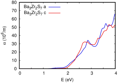
A second consequence of the dimensional reduction is that the optical spectrum is distinctly anisotropic, not only near the band edge as discussed above, but also including significantly anisotropic absorption to above 4 eV in Ba2ZrS4. Ba3Zr2S7 is also anisotropic near the band edge, but is less anisotropic at higher energy, presumably due to the more bulk-like bilayer perovskite block in this compound.
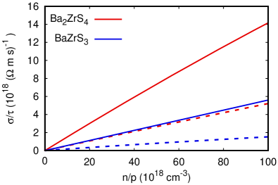
Finally, it of interest to consider the effect of dimensional reduction on the band structures in relation to carrier transport. In general, this requires knowledge of scattering mechanisms for the different compounds and samples along with the temperature dependencies. However, a comparison can be made based on the band structure. Specifically, within the relaxation time approximation for the linearized Boltzmann transport theory, the conductivity, can be expressed as , where is a relaxation time and depends only on the band structure and temperature. We used the BoltzTraP code Madsen and Singh (2006) to calculate this function at 300 K for in-plane transport in Ba2ZrS4 as compared to that in the 3D perovskite, BaZrS3, which is nearly isotropic and for which a direction average is accordingly shown (Fig. 12). Both compounds have higher for electrons than for holes, as might be anticipated from the more dispersive conduction bands, relative to the valence bands. Significantly, the dimensional reduction greatly increases for Ba2ZrS4 relative to BaZrS3 even though the dimensional reduction was accomplished by adding a layer of insulating BaS to the unit cell. Furthermore this enhancement of in-plane transport is clear both for electrons and holes.
IV Summary and Conclusions
First principles calculations for the Ba-Zr-S, RP series show that there is considerable tunability of the electronic and optical properties of BaZrS3 via dimensional reduction. This includes a transition from a direct gap for the perovskite to indirect gaps for the RP phases and reduction of the band gap by up to 0.6 eV. While the perovskite shows a nearly isotropic optical absorption, the RP phases are distinctly anisotropic and different from each other, especially at energies near the absorption onset. In the context of photovoltaics, among the RP phases, Ba2ZrS4 is favorable in terms of band gap, since the difference between the indirect and direct band gaps is relatively small, and the loss of voltage due to the indirect gap might be partly compensated for by an increase in minority carrier lifetime due to suppression of recombination related to the indirect gap. Furthermore, this compound is superior to the 3D perovskite, BaZrS3 from the point of view of in-plane carrier transport. Therefore it is possible that suitably oriented Ba2ZrS4 may be of interest in photovoltaics, in addition to the 3D counterpart BaZrS3. Investigation of the Ba3Zr2S7 would also be of interest. In any case, the substantial electronic tunability by dimensional reduction in these phases may be of important for other electronic applications.
Acknowledgements.
We acknowledge useful discussion with Jayakanth Ravichandran. This work was supported by the Department of Energy, through the S3TEC Energy Frontier Research Center, Award DE-SC0001299. This is work is dedicated to Professor E.K.U. Gross.Author Contribution Statement
Calculations were done by DJS and YL. The manuscript was written by DJS.
References
- Perera et al. (2016) S. Perera, H. Hui, C. Zhao, H. Xue, F. Sun, C. Deng, N. Gross, C. Milleville, X. Xu, D. F. Watson, B. Weinstein, Y. Y. Sun, S. Zhang, and H. Zeng, Nano Energy 22, 129 (2016).
- Niu et al. (2017) S. Niu, H. Huyan, Y. Liu, M. Yeung, K. Ye, L. Blankemeier, T. Orvis, D. Sarkar, D. J. Singh, R. Kapadia, and J. Ravichandran, Adv. Mater. 29, 1604733 (2017).
- Sun et al. (2015) Y. Y. Sun, M. L. Agiorgousis, P. Zhang, and S. Zhang, Nano Lett. 15, 581 (2015).
- Meng et al. (2016) W. Meng, B. Saparov, F. Hong, J. Wang, D. Mitzi, and Y. Yan, Chem. Mater. 28, 821 (2016).
- Robertson (2000) J. Robertson, J. Vac. Sci. Technol. B 18, 1785 (2000).
- Niu et al. (2018) S. Niu, G. Joe, H. Zhao, Y. Zhou, T. Orvis, H. Huyan, J. Salman, K. Mahalingam, B. Urwin, J. Wu, Y. Liu, T. E. Tiwald, S. B. Cronin, B. M. Howe, M. Mecklenburg, R. Haiges, D. J. Singh, H. Wang, M. A. Kats, and J. Ravichandran, Nature Photonics (2018), in press, doi:10.1038/s41566-018-0189-1.
- Kroemer (1963) H. Kroemer, Proc. IEEE 51, 1782 (1963).
- Hicks and Dresselhaus (1993) L. D. Hicks and M. S. Dresselhaus, Phys. Rev. B 47, 12727 (1993).
- Zhang et al. (2016) J. Zhang, L. Song, G. K. H. Madsen, K. F. F. Fischer, W. Zhang, X. Shi, and B. B. Iversen, Nature Comm. 7, 10892 (2016).
- Xing et al. (2017) G. Xing, J. Sun, Y. Li, X. Fan, W. Zheng, and D. J. Singh, Phys. Rev. Mater. 1, 065405 (2017).
- Terasaki et al. (1997) I. Terasaki, Y. Sasago, and K. Uchinokura, Phys. Rev. B 56, 12685 (1997).
- Li et al. (2015) Y. Li, L. Zhang, Y. Ma, and D. J. Singh, APL Mater. 3, 011102 (2015).
- Wang et al. (2012) Q. H. Wang, K. Kalantar-Zadeh, A. Kis, J. N. Coleman, and M. S. Strano, Nature Nanotech. 7, 699 (2012).
- Butler et al. (2013) S. Z. Butler, S. M. Hollen, L. Cao, Y. Cui, J. A. Gupta, H. R. Gutierrez, T. F. Heinz, S. S. Hong, J. Huang, A. F. Ismach, E. Johnson-Halperin, M. Kuno, V. V. Plashnitsa, R. D. Robinson, R. S. Ruoff, S. Salahuddin, J. Shan, L. Shi, M. G. Spencer, M. Terrones, W. Windl, and J. E. Goldberger, ACS Nano 7, 2898 (2013).
- Ohtomo and Hwang (2004) A. Ohtomo and H. Y. Hwang, Nature 427, 423 (2004).
- Parker et al. (2013) D. Parker, X. Chen, and D. J. Singh, Phys. Rev. Lett. 110, 146601 (2013).
- Ruddlesden and Popper (1957) S. N. Ruddlesden and P. Popper, Acta Cryst. 10, 538 (1957).
- Lelieveld and Ijdo (1980) R. Lelieveld and D. J. M. Ijdo, Acta Crysallogr. B 36, 2223 (1980).
- Saeki et al. (1991) M. Saeki, Y. Yajima, and M. Onoda, J. Solid State Chem. 92, 286 (1991).
- Chen et al. (1994) B. H. Chen, B. W. Eichhorn, and N. W. Wong, Acta Crysallogr. C 50, 161 (1994).
- Chen et al. (1993) B. H. Chen, N. W. Wong, and B. W. Eichhorn, J. Solid State Chem. 103, 75 (1993).
- Shannon (1976) R. D. Shannon, Acta Cryst. A32, 751 (1976).
- Singh and Nordstrom (2006) D. J. Singh and L. Nordstrom, Planewaves Pseudopotentials and the LAPW Method, 2nd Edition (Springer, Berlin, 2006).
- Blaha et al. (2001) P. Blaha, K. Schwarz, G. Madsen, D. Kvasnicka, and J. Luitz, WIEN2k, An Augmented Plane Wave + Local Orbitals Program for Calculating Crystal Properties (K. Schwarz, Tech. Univ. Wien, Austria, 2001).
- Perdew et al. (1996) J. P. Perdew, K. Burke, and M. Ernzerhof, Phys. Rev. Lett. 77, 3865 (1996).
- Tran and Blaha (2009) F. Tran and P. Blaha, Phys. Rev. Lett. 102, 226401 (2009).
- Koller et al. (2011) D. Koller, F. Tran, and P. Blaha, Phys. Rev. B 83, 195134 (2011).
- Singh (2010) D. J. Singh, Phys. Rev. B 82, 205102 (2010).
- Madsen and Singh (2006) G. K. H. Madsen and D. J. Singh, Comput. Phys. Commun. 175, 67 (2006).
- Zagorac et al. (2017) D. Zagorac, K. Doll, J. Zagorac, D. Jordanov, and B. Matovic, Inorg. Chem. 56, 10644 (2017).
- Polfus et al. (2015) J. M. Polfus, T. Norby, and R. Bredesen, J. Phys. Chem. C 119, 23875 (2015).
- Sun and Singh (2016) J. Sun and D. J. Singh, APL Mater. 4, 104803 (2016).
- Lax (1974) M. Lax, Symmetry Principles in Solid State and Molecular Physics (Wiley, New York, 1974).
- Shockley and Queisser (1961) W. Shockley and H. J. Queisser, J. Appl. Phys. 32, 510 (1961).