Analysis of the Common Emitter Amplifier Taking into Account Transistor Non-Linearity
Abstract
The operation of a typical common emitter amplifier, including negative feedback, is studied taking into account the non-linearity characteristic of real-world transistors. This has been accomplished by employing a recently proposed Early modeling approach, which allowed the analytical equations to be obtained describing the current and voltage behavior in the adopted common emitter circuit. Average and dispersion (coefficient of variation) of the current and voltage gains can then be calculated and used to characterize the common emitter amplification while reflecting the transistor non-linearity. Several interesting results were obtained, including the fact that the negative feedback provided by the emitter resistance is not capable of completely eliminating effects of parameters differences exhibited by transistors. Importantly, transistors with larger Early voltage magnitudes tended to provide significantly enhanced linearity even when substantial negative feedback is used. These results motivates customized design, implementation and application approaches taking into account the parameters of the available devices.
“’
Delphic Proverb
I Introduction
The common emitter design is one of the most fundamental amplifying circuit configurations, representing a reference in electronics circuits be it for its central role in research, application, or education. This circuit configuration can be found in virtually almost every textbook on electronics circuits (e.g. pettit:1961 ; gray:1969 ; gronner:1970 ; sedra:1998 ; jaeger:1997 ; boylestad:2008 ; horowitz:2015 ; streetman:2016 ). Consequently, much has been said and written about this configuration, including its electronic properties as voltage gain, input and output resistance, linearity/distortion, the negative feedback action implemented by the emitter resistance, stability with component variations, frequency response, to name a few among a set of issues encompassing a great deal of the main interests in electronics. This circuit typically includes a voltage source attached through a capacitor to voltage divider driving the amplifier input port, an emitter resistance for negative feedback shared by both the input and output mesh, and a resistance load in series with an external voltage supply. Either the input voltage or current are taken as the input signal, while the collector voltage, or that across the load, are often understood as the output signal.
The main purpose of the common emitter amplifier is to produce current and/or voltage gain over the load or output, while affecting as little as possible the signal shape. The intrinsic parameter variability exhibited by real-world transistors, allied to the need to improve amplification linearity and stability, motive the incorporation of the emitter resistance as a means to implement negative feedback. However, it is also possible (at the expense of some stability loss) to consider variations of the classic common emitter configuration devoid of the emitter resistance, which can be considered as a means to maximize gain and achieve wider voltage excursion across the load (i.e. avoid the voltage drop at the emitter resistance).
Typically, studies of the common emitter circuit involve the adoption of a model and respectively implied equivalent circuit to represent the involved transistor. The most often employed approaches rely on two electronically meaningful parameters, namely the current gain and the output resistance . This type of approach, however, cannot take into account the nonlinearities that are unavoidably found in any real-world transistor. These nonlinearities are a direct consequence of the fanned structure of the base current () indexed characteristic isolines of the transistor behavior along its operation space , where ad stand for the collector voltage and current.
The above described geometrical organization of transistors action is a sole and direct consequence of the Early effect (e.g. early:1952 ; jaeger:1997 ; streetman:2016 ), in which the base width varies in terms of the voltage applied to the base-collector junction. This effect implies mots of the -indexed characteristic isolines to cross at the same point along the axis. An immediate implication is that the collector output resistance will depend on . Another critically induced property regards the fact that the local current gain , as well as the output resistance become a function of both and . Consequently, transistor modeling approaches relying on and as parameters need to consider their respective averages or point values. Frequently, it is assumed that the fanned isolines can be approximated by a series of equispaced, parallel isolines with the same inclination small . As such, this simplified device is typically represented by an equivalent circuit involving a variable current source in parallel with a fixed output resistance. As an inevitable consequence, this transistor model becomes intrinsically linear, which is a severe simplification of what really happens in real-world transistors.
Recently costaearly:2017 ; costaearly:2018 ; germanium:2018 ; costaequiv:2018 , an alternative transistor model was proposed that is simple and yet can accurately account for the representation of the transistor non-linearities induces by the fanned (or radiating) characteristic isolines. In addition, the two parameters used in this model, namely the Early voltage and a proportionality constant , are constant for any given device, not depending of or . These distinguishing features are allowed by taking into account the very Early effect that causes the fanned isolines as the geometrical basis of the model. Actually speaking, this model also relies on another hypothesis, verified experimentally for hundreds of small signal BJTs costaearly:2017 ; germanium:2018 ; costaearly:2017 , that the angles of the radiating isolines with the horizontal () axis are directly proportional to through the proportionality constant , i.e. , implying that . As is usually very small, in the order to , it is often possible to make with minimal deviation, so that .
Despite its recent introduction, the Early model has already been successfully applied to achieve more complete and accurate modeling and studies of: stability with respect to voltage supply oscillations costaequiv:2018 , parallel combinations of transistors costaequiv:2018 , characterization of the output resistance and current gain of silicon and germanium NPN and PNP small signal transistor models costaearly:2018 ; germanium:2018 , study of a simplified common emitter configuration costaearly:2018 , investigation of complementary transistor pairs in push-pull circuits costaearly:2018 , as well as the characterization of the effects of reactive loads in amplification costareact:2018 , among other results. The Early approach has also allowed the identification of the fact that the amplification in a simplified common emitter amplifier tends to be perfectly linear for very small resistive loads costareact:2018 . In addition, it has been found costaearly:2018 ; costaearly:2018 ; costareact:2018 that the linearity of the transistors amplification devoid of feedback tends to depend only of (directly), and not of . As a matter of fact, the simplicity and completeness of the Early model in being able to represent in an inherently suitable geometrical way the non-linearities of real-world transistors pave the way to a large number of implications for transistor amplification and even linear electronics in general.
The current work focuses on substantially extending previous analyses costaequiv:2018 ; costareact:2018 that had addressed a simplified version of the common emitter configuration. In those works, the emitter was connected directly to ground, and there was no voltage divider for polarization at the input port, so no negative feedback can be achieved. Though that configuration was still representative of several characteristics of transistor amplification, leading to the identification of a series of interesting effects as listed above, it did not account for the negative feedback afforded by the inclusion of an emitter resistor . This is very important because much of modern electronics has relied on negative feedback, introduced by H. S. Black black:1934 , in order to achieve improved linearity and stability to factors such as temperature and transistor parameter variations. These advantages are achieved at the expense of substantial gain expense. Yet, a recent study costafeed:2017 ; costaearly:2018 considering several types of commercial small signal BJTs suggested that negative feedback may not be enough, in several situations, to completely eliminate the relatively large parameter variations exhibited by real-world devices. It was also shown that negative feedback can introduce unwanted harmonics for certain types of non-linearities.
The key role of negative feedback and the common emitter amplifier in electronics, allied to the above mentioned recent findings suggesting some respective limitations, motivate a reappraisal of the classic common emitter amplifier configuration. Of particular interest would be to investigate the efficacy of negative feedback in minimizing transistor non-linearity with respect to different transistor characteristics. For instance, will feedback work more effectively for transistor with large or small current gains or by choosing different values for the external circuit components? If such differences can be found, how much can feedback action be improved by starting with a more linear transistor? How will these effects vary with the intensity of the negative feedback, as set-up by the external resistors? These correspond to key issues in both discrete and integrated circuit analysis, design, implementation and applications. These questions provide the main motivation and objectives of the present work.
We start by presenting the “classic” common emitter configuration, and then obtain a respective equivalent circuit by using the Early modeling methodology. Accurate mathematical expressions are obtained that characterize the voltages, currents and gains while taking into account the non-linear behavior of real-world transistors. By using these equations, it becomes possible to investigate in an objective, more complete, and accurate way how the transistor inherent non-linearity influences the efficiency of negative feedback in promoting linear amplification. This is done by considering the voltage gain average and coefficient of variation (closely related to the level of non-linearity in the amplification) A number of interesting respective results are obtained and discussed, and the work is concluded by presenting some possibilities for further related research.
II The Classic Common Emitter Configuration
Figure 1 shows the configuration of what we will henceforth refer to as the “classic” common emitter circuit. A voltage divider (resistors and ) is used to bias the input port, which is driven by an external signal voltage source , attached through the decoupling capacitor . The load is connected between the collector and the external voltage supply , while resistor is connected between the emitter and ground in order to provide negative feedback. In this circuit, the base-collector junction of transistor is inversely biased, while the junction base-emitter is dforward biased.
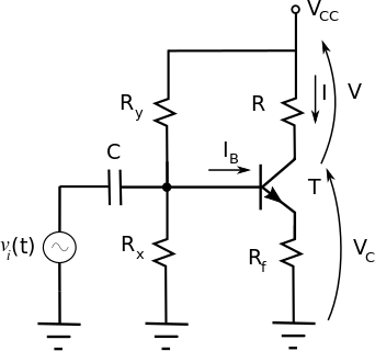
First, we derive the equations for the input port, assuming that the forward-biased base-emitter junction is modeled as a diode with offset voltage and resistance . By using Thevenin’s theorem, we obtain the respective equivalent circuit for the input voltage and divider as:
| (1) | |||
| (2) |
Figure 2 shows the common emitter circuit in Figure 1 modified to show the input port equivalent circuit as well as the output mesh, with the transistor replaced by its Early equivalent circuit. Observe that the input voltage source is not considered as it acts differentially in the amplification, oscillating around the operation point . As is typically very close to ( is much larger than ), it becomes possible to include in series along the input mesh, for simplicity’s and generality’s sake, at the expense of nearly negligible error.
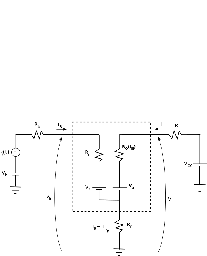
For simplicity’s sake, the above circuit can be further simplified to the configuration shown in Figure 3. This has been achieved by subsuming the input and output series resistances and voltage sources, i.e. , , , and, in particular:
| (3) |
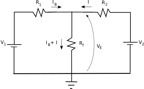
Despite its seeming symmetry and simplicity, this circuit exhibits some relative complexity as a consequence of being a function of , i.e. . The variables in this circuit are , and . By applying Kirchhoff’s and Ohm’s law, we have:
| (6) |
| (7) | |||
| (8) | |||
| (9) |
These equations describe the operation, in terms of (and hence , through Equation 3), of classic common emitter circuit as in Figure 1.
Proper operation of this circuit requires the conditions in Equation 10 and 11 to be obeyed at all times in order to avoid cut-off or saturation (for simplicity’s aske, the Early geometric representation is here understood to cover the whole first quadrant, so that saturation and cut-off occurs at the and axes, respectively.
| (10) | |||
| (11) |
As already observed, despite the seeming simplicity of the system of equations 6, the behavior of the common emitter configuration turns out to be relatively complex. However, Equations 7 and 8 can be conveniently used for obtaining almost any information about the common emitter circuit. In this work, we will focus on two particularly characteristics of this circuit, namely its AC voltage and current gain in terms of the average and coefficient of variation of these gains.
First, we obtain the expressions for the AC current gain. This is done by defining the reference and values for the quiescent point as:
| (12) | |||
| (13) |
so that:
| (14) |
The two indices of interest can now be determined by calculating the average and standard deviation of , i.e. and .
The voltage gain on the load can now be directly expressed as:
| (15) |
Similarly as developed above, this voltage gain can be characterized in terms of its average and standard distribution values and . The respective coefficient are particularly relevant, and are henceforth adopted, as they provide a relative quantification of the gain variation, i.e.:
| (16) | |||
| (17) |
III Analysis in Terms of Circuit Parameters
In this section we apply the obtained equations describing the operation of the classic common emitter amplifier while keeping the transistor parameters and constant and varying the load resistance and the feedback resistance . Recall that the gain variation provides an accurate quantification of the transistor amplification non-linearity, as larger relative variations necessarily imply larger distortions and more intense non-linearity.
In order to derive interpretations for typical small signal NPN and PNP silicon BJT transistors, we use two respective transistor parameters configurations that can often be found experimentally in real-world silicon BJTs costaearly:2018 , i.e. and . As the current gain can be approximated as , these two configurations yield about the same gain, but have widely varying parameters and .
Figure 4 shows the average AC current gain (a) as well as the coefficient of variation of the AC voltage gain (b) with respect to the above mentioned NPN (a-b) and PNP (c-d) configurations.
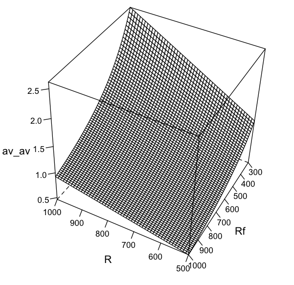
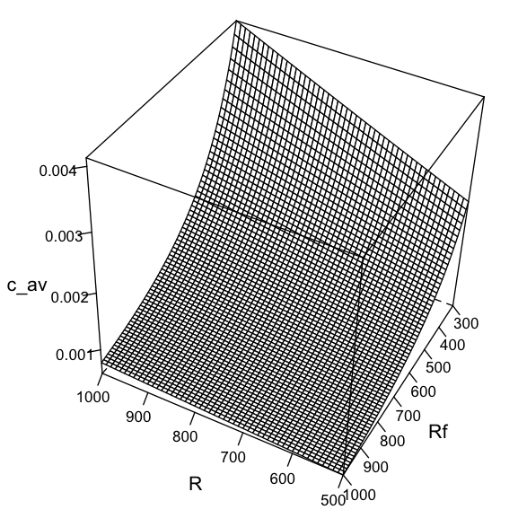
As expected, the two considered parameterizations have nearly the same average gain (Figs. 4(a) and (c)). Observe that the values given by the respective surfaces tend to agree with the less precise estimation of the gain as (note that the quiescent current has been chosen as half the value). The coefficients of variation obtained for the NPN and PNP cases, however, show a marked difference of intensities, despite the fact that the respective surfaces (i.e. Fig. 4(b) and (d)) have very similar shapes. Indeed, the NPN device has over than 3 times less distortion, as a consequence of higher magnitudes typically found in NPN types.
The coefficient of variation of the voltage gain correlates strongly (positively) with the average voltage gain. Both the amplification magnitude and non-linearity increase steadily with and , though tending to increase faster with the latter.
IV Analysis in Terms of Transistor Parameters
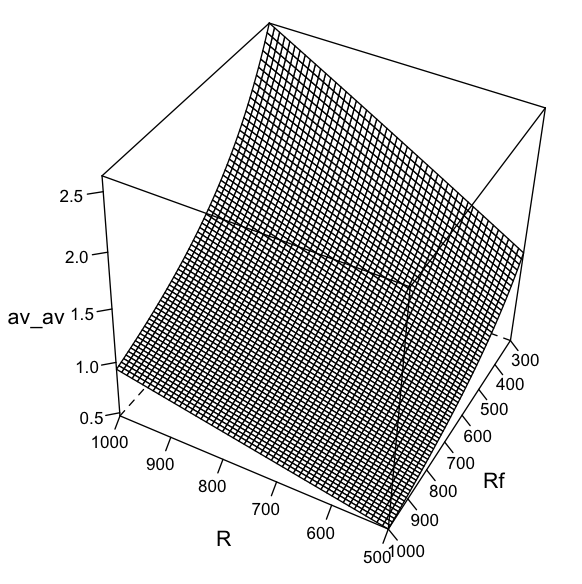
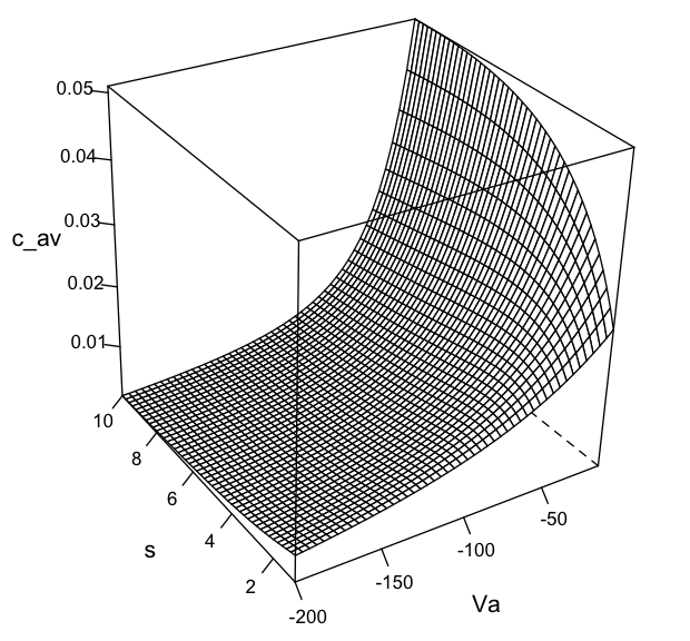
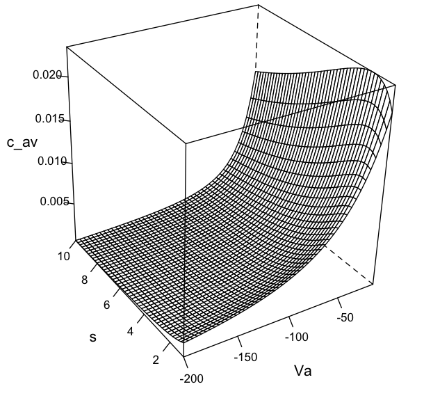
In this section, instead of investigating the behavior of the voltage gain with the circuit parameters and , we fix , take two feedback configurations and , and systematically vary the Early model parameters and . Figure 5 presents the respectively obtained results regarding the averages and coefficients of variation of the voltage gain throughout the Early parameters space .
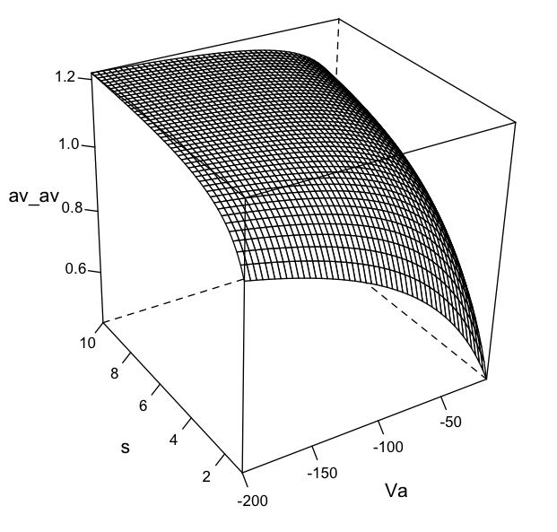
The average voltage gain surfaces resulted with similar shapes, but showing different magnitudes (Figs. 5, with the amplification achieved for the NPN circuit being twice as much higher (approximately at the highest values). A closer inspection reveals that the average gain surface for and has a flatter top than for the other configuration. These surfaces show that the average voltage gain increases steeply with both magnitude and , but then reach a plateau of greater gain uniformity moving toward .
Interestingly, the dispersions of voltage gain (and hence larger non-linearity) verified for and , as shown in Fig. 5(b), present an opposite tendency to that of the average voltage gain. More specifically, the distortion decreases with both and , with this decrease being markedly more accentuated with increase of the magnitude. A well-defined flat valley of linearity is obtained around . Observe that this valley mostly coincides with the gain peak plateau, suggesting that the available open loop gain has been traded for increased linearity.
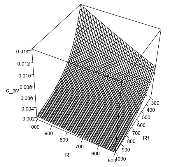
The coefficients of variation obtained for the case and (Fig. 5 (d)) resulted distinct in the sense that the distortion mostly decreases as becomes larger. This has the interesting implication that transistors with larger values of will tend, for such situations, to yield less distortion for this specific configuration of and .
Perhaps the most important overall implication of the above discussed results is the fact that, even in presence of relatively high feedback levels (e.g. ), when almost all gain is traded-off for linearity and stability, the linearity of the amplification still varied substantially with different values of the transistor parameters and . This finding corroborates, for the considered configuration and ranges, the previously observed phenomenon costafeed:2017 ; costaearly:2017 that negative feedback may not be capable of completely eliminating transistor parameter variation. Therefore, it becomes an interesting option to consider the transistor parameters and for circuit design and implementation, even when adopting intense levels of negative feedback.
V Current Gain
Though the common emitter amplifier is typically approached with respect to voltage gain, It is also interesting to consider the AC current gain as can be derived from the analytical Equations 7 and 8.
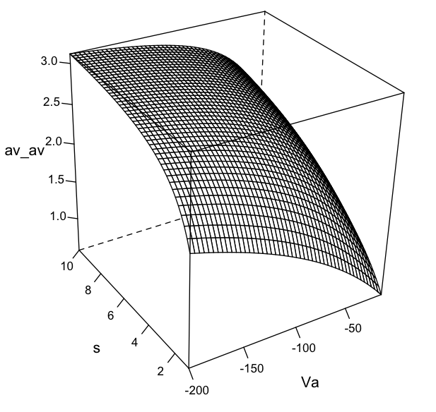
The obtained results are qualitatively similar (though with distinct intensities), so we restrict our discussion to the analysis of the average current gain throughout the space , as observed for and , which is depicted in Figure 6.
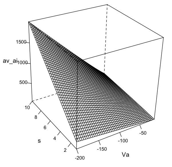
This result shows that the average current gain for the mentioned configuration increases in an almost linear way with both and , reaching its peak of nearly 2000 at . Though a direct consequence of the circuit operation dynamics, it is interesting to observe that the average current and voltage gains depend in such distinct ways on the parameters and .
VI Concluding Remarks
Amplification is a key issue in analog/linear electronics because of the non-linearity that is inherent to any real-world amplifying devices such as transistors. As such, much effort has been invested in devising circuits and techniques capable of achieving satisfactory performance under specific circumstances. The common emitter circuit is probably the “quintessential” amplification approach in electronics, acting as a reference for other designs and development of novel techniques aimed at improving amplification, as is the case of negative feedback.
The non-linearity inherent to junction transistors stems mostly from the Early effect, which implies the base current-indexed isolines characterizing the typical amplification to converge into a single point along the axis. The recent introduction of the Early modeling approach costaearly:2017 ; costaearly:2018 ; germanium:2018 ; costaequiv:2018 paved the way to more systematic, analytical investigations of the behavior of amplifying circuits, including the common emitter configuration. In addition to its inherent simplicity, these approaches are capable of taking in to account the transistor non-linearity as stemming from the radiating characteristic isolines implied by the Early effect. Preliminary approaches to common emitter amplification were reported recently costaequiv:2018 ; costareact:2018 , but those approaches took into account a simplified common emitter configuration devoid of negative feedback. Even so, it was possible to achieve several interesting results, including the relatively severe effect of the transistor non-linear amplification, as well as its great dependence on the transistor Early parameters and .
The present work addressed the complete, classic common emitter configuration, incorporating voltage divider-based input biasing and, more importantly, negative feedback as provided by a resistance attached between the collector and the ground. This resistance has to be kept at relatively small values in order not to reduce too much the current and voltage amplification too much. The approach reported here takes into account the transistor non-linearity implied by the Early effect, allowing the study of how effectively negative feedback can enhance linearity.
The reported analysis was developed as follows. First, the equivalent circuit of the classic common emitter configuration was derived by using electrical circuit laws and the Early voltage equivalent circuit for a transistor in amplifying mode. The base current and collector current were treated as functions of the input voltage . Analytical solutions were obtained for and , providing the complete electrical description of the considered common emitter amplifier. The average, standard deviation, and coefficient of variation of the voltage and, to a smaller extent, current amplification (gains) were obtained and used for investigating the effect of several circuit and transistor parameter configurations. As gain variations are closely related to non-linearities, it was possible to address both the overall gain, as expressed in terms of the average of the gains obtained along excursions, as well as to infer the respective linearities.
Several interesting results have been reported. First, we have that the choices of the load and feedback resistance (circuit components) can influence strongly both average gain (as expected) and linearity. Importantly, these gains were found to vary with even in presence of relatively intense negative feedback, implying amplifying distortion. Perhaps more importantly, the transistor inherent characteristics and were found to strongly influence the linearity of the amplification even in presence of relatively high negative feedback. Similar results had been experimentally observed recently costafeed:2017 ; costaearly:2018 . By providing a more complete and accurate analytical framework to characterize the common emitter circuit, the present work not only confirmed those preliminary experimental indications, but also showed in a more systematic and conclusive way that, though certainly remaining an interesting option, negative feedback is not enough to completely eliminate effects of transistor parameter variations. This important fact implies that, especially in particularly critical circumstances, it may be worth taking into account the specific characteristics of available real-world transistors. Another interesting result concerns the fact that the linearity can increase or decrease according to for different and configurations.
The implications of the above results are several and have great potential for motivating many related further investigations, including the study of higher power amplifiers, consideration of reactive loads, as well as the systematic study and characterization of other important electronic circuits such as current mirror, phase splitters, and differential amplifiers, up to complete operational amplifier configurations, to name but a few possibilities.
Acknowledgments.
Luciano da F. Costa thanks CNPq (grant no. 307333/2013-2) for sponsorship. This work has benefited from FAPESP grants 11/50761-2 and 2015/22308-2.
References
- (1) H. S. Black. Stabilized feedback amplifiers. Bell System Technical Journal, (1):1– 18, 1934.
- (2) L. da F. Costa. Characterizing complementary bipolar junction transistors by early modeling, image analysis, and pattern recognition, 2018. arXiv preprint arXiv:1801.06025.
- (3) L. da F. Costa. Characterizing germanium junction transistors, Jan. 2018. https://archive.org/details/Germanium.
- (4) L. da F. Costa. On the effects of resistive and reactive loads on signal amplification, Feb 2018. arXiv preprint arXiv:1802.02279.
- (5) L. da F. Costa. Towards a simple, and yet accurate, transistor equivalent circuit and its application to the analysis and design of discrete and integrated electronic circuits, 2018. https://archive.org/details/reactive_201802.
- (6) L. da F. Costa, F. N. Silva, and C. H. Comin. Electrical Engineering, (3):1139, 2017.
- (7) L. da F. Costa, F.N. Silva, and C.H. Comin. An Early model of transistors and circuits, 2017. arXiv preprint arXiv:1701.02269.
- (8) J.M. Early. Effects of space-charge layer widening in junction transistors. Proceedings of the IRE, (11):1401–1406, 1952.
- (9) P. E. Gray and C. L. Searle. Electronic Principles: Physics, Models and Circuits. John Wiley and Sons, 1969.
- (10) A. D. Gronner. Transistor Circuit Analysis. Simon and Schuster, 1970.
- (11) P. Horowitz and W. Hill. The Art of Electronics. Cambridge University Press, 2015.
- (12) R. C. Jaeger and T. N. Blalock. Microelectronic Circuit Design. McGraw-Hill New York, 1997.
- (13) Boylestad R. L and L. Nashelsky. Electronic Devices and Circuit Theory. Pearson, 2008.
- (14) J. M. Pettit and M. M. McWhorter. Electronic Amplifier Circuits: Theory and Design. McGraw-Hill, 1961.
- (15) A. Sedra and K. Carless Smith. Microelectronic circuits. Oxford University Press, New York, 1998.
- (16) B. G Streetman and S.K. Banerjee. Solid State Electronic Device. Pearson, 7th edition, 2016.