On the Effects of Resistive and Reactive Loads on Signal Amplification
Abstract
The effects of reactive loads into amplification is studied. A simplified common emitter circuit configuration was adopted and respective time-independent and time-dependent voltage and current equations were obtained. As phasor analysis cannot be used because of the non-linearity, the voltage at the capacitor was represented in terms of the respective integral, implying a numerical approach. The effect of purely resistive loads was investigated first, and it was shown that the fanned structure of the transistor isolines can severely distort the amplification, especially for small and large. The total harmonic distortion was found not to depend on , being determined by and the load resistance . An expression was obtained for the current gain in terms of the base current and it was shown that it decreases in an almost perfectly linearly fashion with . Remarkably, no gain variation, and hence perfectly linear amplification, is obtained when , provided maximum power dissipation limits are not exceeded. Capacitive loads imply the detachment of the circuit trajectory from a straight line to an “ellipsoidal”-like loop. This implies a gain asymmetry along upper or lower arcs of this loop. By using the time-dependent circuit equations, it was possible to show numerically and by an analytical approximation that, at least for the adopted circuit and parameter values, the asymmetry induced by capacitive loads is not substantial. However, capacitive loads will imply lag between the output voltage and current and, hence, low-pass filtering. It was shown that smaller and larger can substantially reduce the phase lag, but at the cost of severe distortion.
“There is geometry in the humming of the strings.”
Pythagoras
I Introduction
The dynamics of the natural world is underlain by myriad signals covering all scales of magnitude. From the light of the faintest star to the sound of the loudest thunder (not to mention quarks and supernovae), signals permeate and integrate the whole universe. From Pitagora’s time, it has been known that natural signals (in that case, sound) can be understood in terms of basic harmonic functions, each with a respective magnitude. Interestingly, the way in which signals are changed by environment, such as the propagation of a bird songs throughout a forest, can be understood as changes, in specific ways, in the magnitudes of each of the signal harmonic components. For simplicity’s sake, these signal magnitude alterations are henceforth called amplification, even when the resulting signal has its amplitude reduced. So, it can be said that a good deal of signal processing resumes to magnitude alterations. It is consequently hardly surprising that the development of science and technology has relied so much on the acquisition, amplification and analysis of signals. Indeed, all instruments critical for measuring nature, from microscopes to telescope arrays, require accurate, reliable and linear amplification of signals. A very much similar situation is found regarding the vast majority of human activity: linear signal amplification is required in telecommunications, health/leisure, and transportation, among many other critical areas. Interestingly, sometimes humans also aim for non-linear amplification, as is the case with music instrument synthesis.
Analog (or linear) electronics (e.g. analogdesign:1988 ; analogdesign:1991 ), more recently accompanied by digital amplification (e.g. menchi:2016 ), is the main scientific-technologic area focusing on the amplification of natural signals. It has provided the foundation for much of instrumentation used in science and technology. The main goal here often is to achieve as much linear operation as possible, which is a rather challenging issue given the intrinsically non-linear nature of real-world components, such as transistors. Interestingly, our world is predominantly non-linear, being rather difficult to think of natural phenomena that are perfectly linear. At the same time, most of our approaches to science, at least until recently, relied on mapping non-linear real-world phenomena into approximated linear representations. This also happened with transistor studies, as often (but not always) these devices have been mapped into linear respective representations.
Indeed, because of its many important and critical applications, much effort has been invested in deriving effective approaches to transistor characterization, representation and modeling (e.g. stewart:1956 ; jaeger:1997 ; sedra:1998 ; horowitz:2015 ; streetman:2016 ). Though in the beginning, especially from the 50’s to the 70’s, these efforts tended to focus on graphic and analytical approaches — with extensive use of characteristic curves, surfaces, and transfer functions (e.g. shea:1955 ; zimmermann:1959 ; pettit:1961 ; fontaine:1963 ; alley:1966 ; gronner:1970 ; tinnell:1972 ), the progressive extension to larger and more complex integrated devices was largely assisted by more systematic application of numeric computational simulations. Yet, continuing research into more analytical approaches to transistor characterization, representation and modeling remains an important issue as it can not only extend our intuitive understanding of transistor operation, but also contribute do more effective and accurate simulation approaches and tools. Recently, a simple transistor model, as well as its respective equivalent circuit, was developed costaearly:2017 ; costaearly:2018 ; costaequiv:2018 that is founded on the Early effect, discovered by J. M. Early in 1952 early:1952 ; ziel:1968 ; streetman:2016 . Despite its great simplicity, consisting of a Thevenin configuration with a fixed voltage source in series with a variable resistance ( is the current base, and a proportionality parameters), this model exhibits two interesting and important features: (i) it allows the representation of the transistor varying output resistance in terms of the modulating base current (corresponding to the fanned isolines that are so characteristic real-world transistor graphic representations); and (ii) the two involved parameters, namely and do not vary with the transistor operation as quantified by the collector current and voltage . Recall that both the parameters and adopted in many traditional transistor modeling approaches are explicit functions of and , i.e. and . This parametric dependence implied that averages, or other functionals, of these two parameters had to be used for the characterization of transistor properties costaearly:2018 , implying in specific or arbitrary choices about in which domain to integrate the parameters and into respective averages and .
Despite its recent introduction, the Early modeling approach has already led to interesting results, such as the characterization of typical properties of NPN and PNP bipolar junction transistors (BJTs) costaearly:2018 , the study of germanium alloy junction devices germanium:2018 , the derivation of a prototypic parameter space characterizing trade-offs between gain and linearity costaequiv:2018 , the study of stability of circuit operation under voltage supply oscillations costaequiv:2018 , as well as the derivation of the Early equivalent model of parallel transistor configurations costaequiv:2018 . The aforementioned study of circuit stability involved a comparison with a more traditional simplified modeling approach, which showed that largely divergent results can be obtained when considering or not the fanned structure of the base current-indexed isolines, and justifying the use of models such as the Early approach. Indeed, the development of an equivalent circuit for the Early model costaequiv:2018 paved the way to applying this modeling approach to a large number of relevant problems regarding transistor characterization, modeling, simulation, and design in discrete and integrated electronics.
The present work addresses the issue of transistor amplification in circuits involving reactive loads, a situation very commonly found in practice. While purely resistive loads imply a straight line in the transistor characteristic surface, capacitive or inductive loads will define “ellipsoidal”-like pathways in these parametric spaces, also implying phase shifts between the current and voltage at the load. While these alterations would still lead to linear amplification were the transistor a linear device (i.e. had parallel, equispaced current modulated-isolines), the fanned structure actually observed in real-world devices implies that the achieved amplification will become non-linear not only because the load line will no longer be straight, but also because different paths will be followed for the positive and negative portions of the amplified signal. The fact that the induced phase shifts depend on the frequency of the input signal complicates further the situation. The availability of the Early model and respective equivalent circuit provides a viable and yet accurate way to approach this interesting and important problem of non-linear amplification considering reactive loads, and this constitutes the main motivation of the current work.
A simplified common emitter configuration is adopted in which there is no emitter resistance (no negative feedback) and the load is attached between the transistor collector and the external voltage supply . By using the Early equivalent circuit costaequiv:2018 , it was possible to obtain the time-independent and time-dependent equations for the currents and voltages in the adopted circuit. The case of purely resistive loads is studied first by using the respective time-independent circuit equations, which allowed the total harmonic distortion of the amplification to be estimated for each of the possible configurations in a region of the Early space parameter, leading to remarkable results. The case of capacitive loads is studied next, and its effect on linearity and phase lag (low-pass filtering) are studied by using numeric as well as analytical approximations, also with surprising results. The work concludes by identifying prospects for future related research.
II A Simplified Common Emitter Configuration and its Early Model Representation
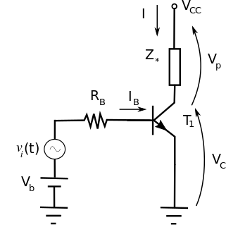
Figure 1 illustrates the simplified common emitter configuration considered in this work, where stands for a generic load with resistive and reactive properties. The adopted circuit configuration is said to be simplified because the base is does not incorporate some features typically found in the common emitter configuration, i.e.: (i) the base is not biased by a voltage divider, and the input signal is driven through a base resistance ; (ii) there is no resistance between the emitter and the ground, which is often used to achieve negative feedback; and (iii) the load is attached directly between the collector and the external voltage supply , not attached to the collector through an additional decoupling capacitor.
The adopted simplifications, however, do not change much the properties of the circuit with respect to the more traditional common emitter configuration. For instance, collector bias can be incorporated as part of the input current so that, mathematically, the same effect can be achieved. The avoidance of the emitter resistance is compatible with the objective of the present work, which focus on the characterization of the circuit linearity under reactive loads, so that it is more interesting to consider the situation with more distortion. The situation with will be considered in a forthcoming work focusing on the study of negative feedback by using the Early formulation. Regarding simplification (iii), this does not affect the characterization of the linearity of the transistor and the so-developed analysis can be immediately extended to other situations more commonly found in practice, such as attaching the load to the collector via a decoupling capacitor.
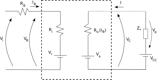
The Early model equivalent circuit costaequiv:2018 can be easily employed to obtain the mathematical equations underlying the behavior of the circuit in Figure 1. First, we replace the transistor by the Early model equivalent circuit costaequiv:2018 , yielding the circuit shown in Figure 2.
The input section is modeled in terms of a diode, as usual, so that we have:
| (1) | |||
| (2) |
Recall that the Early representation of the output port involves two parameters: the Early voltage and a proportionality parameter . One of the distinguishing features of the Early model is that both these parameters do not depend on or . In addition, these parameters have been formally related to averages of the more frequently adopted current gain and output resistance. Interesting, as a consequence of scaling properties of the fanning geometrical structure underlying the Early model, the effective current gain results, in an approximate sense, directly proportional to the product of magnitude and , i.e. . This can be immediately appreciated by considering that: (a) if is doubled, the effective current gain will be halved; (b) if is doubled, this same gain is doubled. So, the net product is not to change the effective current gain. We also have that . It is interesting to perform the circuit analyses and discussions considering distinct parameter configurations leading to the same current gain.
In the respective equivalent circuit costaequiv:2018 , the parameter defines the output resistance that is a function of the base current given a fixed value of . Observe also that takes negative values.
Now we can apply electric circuit analysis, in particular applying Kirchhoff’s and Ohm’s law, to derive equations respectively describing the adopted simplified common emitter circuit. For simplicity’s sake, we first consider a purely resistive load , which yields the follwing time-independent equations:
| (3) | |||
| (4) | |||
| (5) |
The obtained equations are similar in complexity costaequiv:2018 to those obtained for more traditional models based on the current gain and output resistance .
However, a slightly more sophisticate situation arises when we considered reactive loads. Now, because the transistor is non-linear, so that the voltage and current values will vary in a non-linear way as functions of , we cannot use the customary steady state analysis and phasor methods. Instead, we need to substitute the reactive components by their integral or differential formulation, so as to define respective frequency-dependent voltage or current terms in the respective time-dependent circuit equations.
We illustrate this procedure with respect to a capacitive load involving a capacitor in parallel with a resistance , as illustrated in Figure 3.
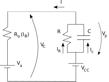
For this configuration it is convenient to consider the voltage formulation for the load, so that we have the following, relatively simple, time-dependent equations:
| (6) | |||
| (7) | |||
| (8) |
At the mesh defined by the load, Kirchhoff’s voltage law yields:
| (9) |
At that same mesh, Kirchhoff’s current law implies that , so that we obtain:
| (10) |
Now we can derive the voltage across the capacitor as:
| (11) |
The so obtained time-independent and time-dependent equations provide all the necessary resources for analyzing the amplification properties of the circuit in Figure 1 while driving purely resistive and resisitive-reactive loads. However, first we provide some considerations regarding the numerical solution of the above circuit.
III A Simple Numeric Approach
Because steady state phasor methods cannot be used to perform AC studies on non-linear circuits with reactive loads, it is necessary to consider other methods. In this work, capacitors or inductors are substituted, as implied by each specific circuit topology, by their respective integro and differential equations, i.e.:
| (12) | |||
| (13) | |||
| (14) | |||
| (15) |
These equations can then be substituted for respective voltages or currents in the circuit, whenever implied by the circuit topology and focus of study. The integrals or differentials are then interactively estimated during the circuit analysis . Let’s illustrate this approach with respect to the circuit in Figure 3. A voltage-based analysis of this circuit yielded Equations 6 to 8. Assuming that the capacitor is initially discharged (i.e. , we can derive the following interactive loop, aimed at obtaining the circuit solution from to , with time resolution :
Observe that this algorithm uses a simple trapezoidal integration scheme, so that more demanding situations may require more precise/sophisticated numeric integration methods (e.g. press:2007 ). In the present work we have used , but this choice needs to take into account the frequency limit and reactance and resistance maximum values, so that larger values o may be required in other parametric configurations.
IV Amplification onto Purely Resistive Loads
Now we proceed to investigate the characteristics of amplification of the circuit in Figure 1 by considering the case of purely resistive loads. The behavior of the circuit for this configuration is given by the time-independent Equations 3 to 5.
We adopt a sinusoidal signal with frequency and amplitude . Figure 4 shows the trajectories defined by the signals and in the circuit operation space for purely resistive loads with values . The adopted parameters defining the transistor operation in these cases were and . These Early parameters values can be found in PNP BJT transistors costaearly:2018 .
Any trajectory for purely resistive loads will be, necessarily, fixed and straight. This is a consequence of the fact that, for this type of load, the circuit operation is restricted to the straight line extending from to . Nevertheless, the obtained trajectories will have inclination equal to , as in Figure 4. So, larger values of will imply smaller transfer function slopes.
Figure 5(a) shows the transfer function lin:2017 defined by the transistor while going from to (i.e. , and Figure 5 (b) shows the superimposition of and , the latter having been scaled to match the amplitude of . It is evident from this figure that the fanned structure of real-world transistors can strongly deform the original signal, as reflected in the bent transfer function and the mismatch between the shapes of the input and output currents. An overall current gain was obtained.
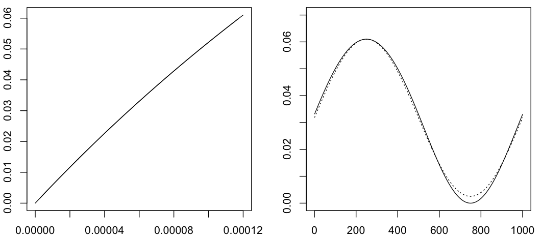
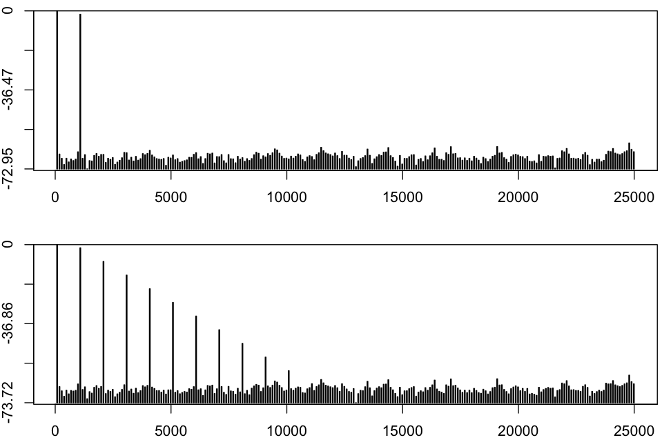
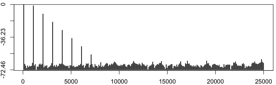
Figure 7 depicts the power spectrum of the original signal (a) and of the amplified signal (b). The distortion implied by the transistor geometry on the lower harmonics is evident. Observe that the residual power spectrum values smaller than are a consequence of numerical round-off noise, and can be disregarded.
Now, we repeat the study above, but considering and , which yields approximately the same current amplification. This parametric configuration can be found in silicon NPN BJTs costaearly:2018 . Figure 6 depicts the respectively obtained transfer function (a) and superimposition of the input and output currents (b).
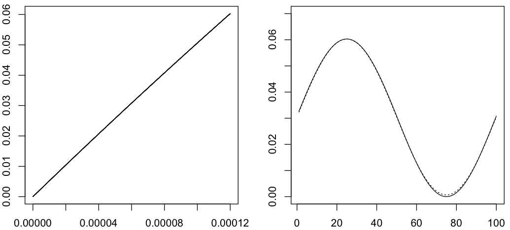
The obtained transfer function resulted substantially less bent for for and , implying in much smaller amplification distortion. This confirms that the Early transistor parameters can have great influence on the amplification linearity. The power spectrum of the output current obtained is shown in Figure 7(c).
The total harmonic distortion (THD) can be employed to effectively summarize the degree of distortion implied by the amplification non-linearities, which incorporate new harmonics into the amplified signal. This index is defined as:
| (16) |
where is the RMS value of the -th harmonic component, and is the RMS value of the fundamental which, in our case, corresponds to the pure sinusoidal input .
The THD, considering only harmonic components with relative intensity larger than , obtained for and was found to be equal to . The THD obtained for the Early parameter configuration and was , yielding the ratio , which is substantial. This result corroborates the fact that the fanned geometric structure underlying real-world transistors can have a major non-linear effect, implying substantial distortion on the amplification. Indeed, this could have been already guessed even by visually comparing the transfer functions obtained for the two considered parameter configurations, as that for and (Fig. 5) is much more bent than that for and (Fig. 6).
Such a strong effect of the transistor Early parameters and on amplification linearity and distortion motivates a more systematic analysis. Figure 8 shows the THD values obtained for , , and amplitude of equal to . These values were estimated by using the derived time-varying equations to obtain the output signals, followed by respective fast Fourier numerical analysis (e.g. brigham:1988 ; shapebook ).
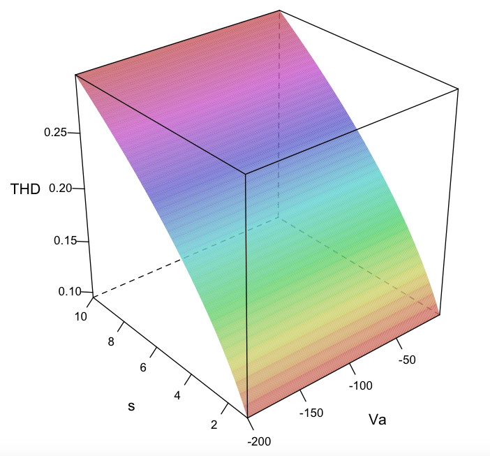
Remarkably, the distortion implied by the transistor inherent non-linearity depends only of the transistor Early parameter , not of . This result is in full agreement with previous Early model investigations of the considered simplified common emitter circuit configuration costaearly:2018 ; costaequiv:2018 . The smaller the value of of a given transistor, the smaller the THD will be, and this is the only effect determining distortion as far as the fanning geometrical organization of the transistor isolines is concerned. However, considering nearly constant current gains , if is reduced, tends to increase. So, linearity can be optimized under the current assumptions by choosing small and large, which is a characteristic of silicon NPN BJTs (see costaearly:2018 ; costaequiv:2018 ). Recall that no distortions at all would have been otherwise observed in case a more traditional model based on current gain and output resistance , with parallel (even though inclined) characteristic isolines had been used.
It can be verified that smaller values of will yield THD surfaces with similar shapes, but with proportionally smaller values. This is a consequence of the fact that, for smaller values of , the load lines will approach the vertical, where the current gains implied by the radiating -indexed isolines are more uniform. This interesting phenomenon is further investigated in the following section.
V Amplification onto Capacitive Loads
The so far obtained results for purely resistive loads corroborate the fact that the non-linearities implied by the fanning structure of the transistor isolines can impinge large distortions on the respective amplification, depending on the Early parameters of the chosen transistors and the load resistivity. Now, we proceed to investigate how this influence takes place when the load incorporates a capacitive element, as in Figure 3.
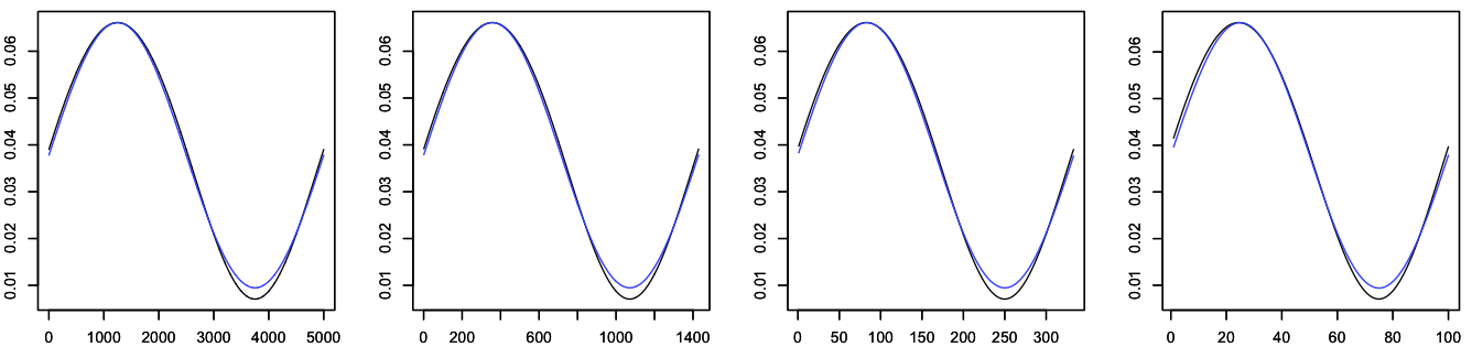
First, let’s consider the effect of a capacitor placed in parallel with a resistive load . Figure 9 illustrates the obtained trajectories defined by and in the circuit operation space for a pure sinusoidal inputs with amplitude and frequencies (a), (b), (c), and (d). This figure also shows (in blue), as a reference, the load line obtained for a purely resistive load . The adopted transistor parameters are and .

The transient dynamics can be observed, proceeding from the initial condition to the steady state regime. As the input frequency increases, the circuit operation progressively detaches from the straight line constraint implied by a pure resistive load, defining “ellipsoidal”-like trajectories. This is a direct consequence of the fact that, in loads defined by resistance in parallel with capacitance, the voltage will be “behind” (or “lag”) the current. However, the non-linearities implied by the fanned transistor isolines preclude the application of phasor analysis typically adopted in linear steady state conditions (e.g. jaeger:1997 ; hyat:1962 ).
Observe that this detachment of the trajectories implies the distortions experienced along the upper trajectory cycle arc to be different from those along the lower arc. Now, it is a particularly intriguing question to investigate how this asymmetry can further impact the amplification non-linearity. Figure 10(a)-(d) shows the input and output signals obtained for each of the four cases in Figure 9 ( and ). Observe that has been suitably scaled up so that its shape can be directly compared to that of .
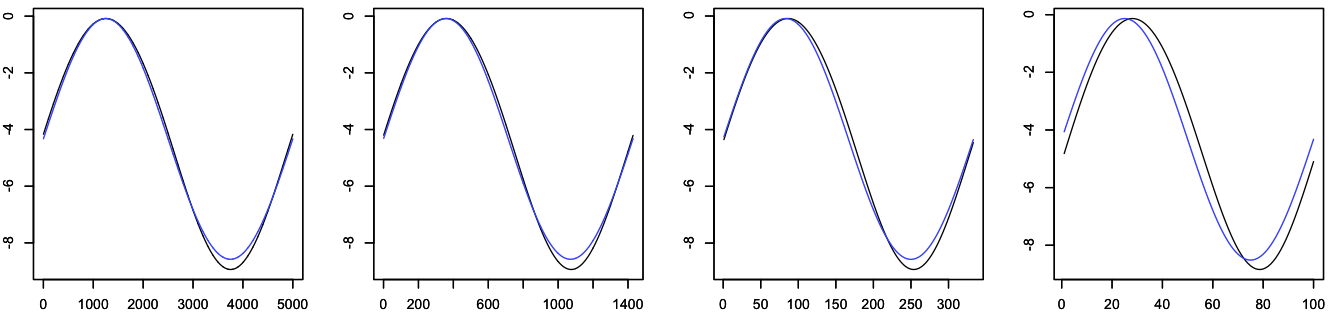
Interestingly, the distortions implied by this circuit configuration are very similar to those observed in Figure 5(b). Indeed, THD comparisons showed that the trajectory asymmetry implied by the capacitive load does not affect significantly – at least for the considered circuit, parameter and variable configurations – the linearity of the amplification. This is an interesting phenomenon that can be further investigated analytically by using two parallel purely resistive load lines, as in Figure 11 to approximate the gain variation as the trajectory excursions along the upper and lower arcs of the loop. Observe that the displacement of these load lines is defined by the supply voltage .

We have from the Early modeling of the considered circuit with a purely resistive load has its output current expressed as:
| (17) |
It follows that the current gain along the load line, in terms of is given as follows:
| (18) |
Observe that this current gain is a function of the transistor Early parameters and as well as the circuit parameters , and , as well as . Now, we take the output current along a load line parallel (same ) to the previous one. This new load line has it position along the horizontal axis determined by , where is a proportionality coefficient (e.g. ):
| (19) |
The current gain along this load line, in terms of , can be derived as:
| (20) |
Now we can obtain the proportion between the current gain between the second and first load lines as:
| (21) |
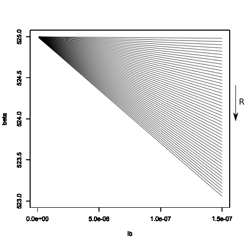
Remarkably, turns out to be independent of , and , varying only with , and . This is shown in Figure 12 for , where successive constant gains are obtained for steps of .
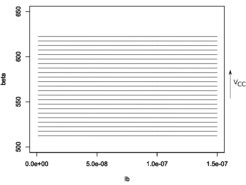
Figure 13 illustrates the current gain in terms of , for . As a consequence of the -indexed fanned characteristic of the isolines underlying the transistor operation, the current gain varies in a virtually linearly decreasing way with for all considered values of . Remarkably, as less gain variation implies in enhanced linearity, almost perfect linear amplification is achieved for loads with very smal . Indeed, perfect linear operation is achieved in the limit , provided is controlled so as to have not exceeding the voltage supply maximum current and the transistor maximum power dissipation.
Now, substituting for , and , we have that . For a good average gain (NPN) , this implies in a relative gain variation of , which is negligible given the typically obtained values of gains, parameters and variables for the considered configurations.
So, for the considered hypothesis and configurations, the capacitive component of the load does not strongly influences the linearity of the amplification despite the respectively implied asymmetry along the upper and lower arcs of the loop. This happens particularly for large values of , which is known costaearly:2017 ; costaearly:2018 ; costaequiv:2018 to be directly related to the transistor average output resistance , irrespectively of . So, transistors with larger values of not only will have better linearity for a same gain, but will also (and for the same reasons) imply better resilience to capacitive load effects. However, large output resistance also implies bigger lag between the output voltage and current, and hence typically unwanted low-pass filtering, which is another important aspect deserving further consideration.
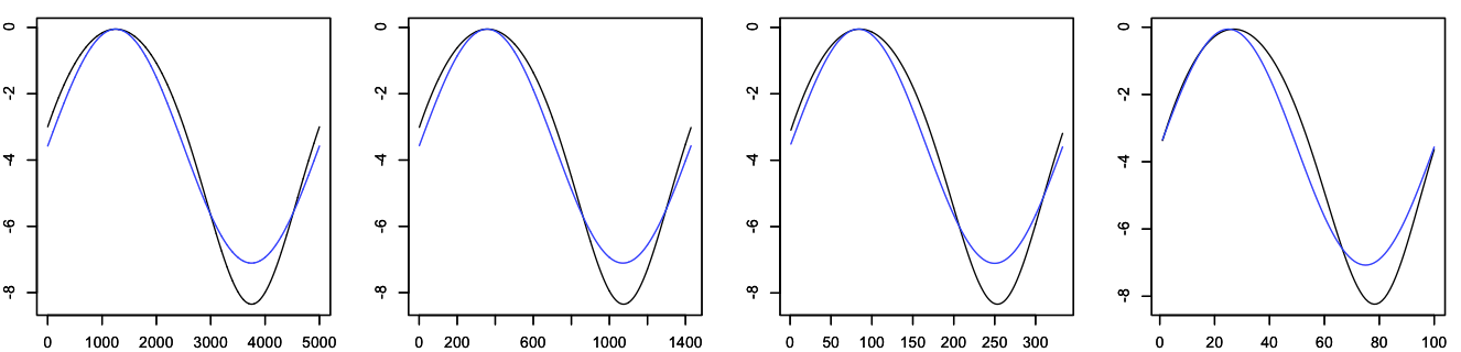
Figures 10(e)-(h) show the collector voltage superimposed onto the input current , with respect to (e), (f), (g), and (h), assuming and . Observe that had to have its signal inverted, and then was scaled up so as to allow the comparison between the shape of these two signals. Unlike what was verified between the input and output currents, which is always in phase, there is a very perceptible lag between the output voltage and current that increases with , even though this is not a particularly high frequency. So, the choice of large values of implies larger average output resistance that tends to worsen the lag, implying more intense low-pass filtering. So, a trade-off is revealed between linearity and low-pass filtering implied by capacitive loads. This tends to become particularly critical for loads with large resistive or capacitive components (i.e. large ).
Because filtering represents a distortion of the original signal, it is important to try to devise means for avoiding the effects of capacitive loads. An immediate possibility is to use transistors with smaller , leading to smaller average output resistance . Figures 10(i)-(l) depict the output voltage and input current for and (same gain as before, but much smaller output resistance), with respect to (e), (f), (g), and (h). Though a large distortion has been implied to the voltage signal, the smaller output resistance allowed by allowed an almost perfect phase match between the input current and the output voltage . However, the severity of the impinged distortion renders this solution unviable for most applications, except as a possible means of dealing with synchronization problems.
Another possibility to avoid the complications implied by capacitive loads is to add an inductor in series with the load, with reactance perfectly matched so as to cancel the load capacitance (in a manner remindful of load correction), yielding a purely resistive load as a result. Interestingly, the compensation required for any given signal frequency will also work for other frequencies. This possible technique is allowed as a consequence of the transistor non-linearities having been found in this work, at least for the considered hypotheses, not to influence too much the asymmetry of the amplification along the two arcs of reactive loops, otherwise the compensation could be undermined. This possible technique also requires the capacitance to be canceled not to be a function of other parameters (e.g. voltage, electromagnetic field or temperature) than the signal frequency.
VI Concluding Remarks
Linear amplification remains a critically important issue for a vast number of electronics applications required by science/technology and as assistance to humans. However, the non-linearity intrinsic to transistors has substantially constrained more systematic and complete studies of transistor-based amplification. The recent development of a simple and yet accurate transistor model costaearly:2017 ; costaearly:2018 ; costaequiv:2018 capable of incorporating the key non-linearities characterizing the operation of these devices, paved the way to allowing more accurate studies of transistor amplification. One particularly relevant and challenging aspect related to the non-linearity of transistor amplification concerns the influence of loads with reactive components on the circuit operation. This issue has been particularly complicated to be approached because of the lack of simple and accurate transistor models capable of reflecting the fanned structure of the characteristic surface of real-world transistors. This structure implies non-linearities precluding the complex phasor approach commonly used in AC circuit analysis to be used. To address this problem in a more systematic way provided the main motivation for the present work.
A simplified common emitter circuit configuration was adopted and represented in terms of its Early model, which involves only two parameters, and , that are invariant to the circuit operation as defined by the base current , collector current and collector voltage . The Early equivalent circuit of a transistor was then applied to derive simple, and yet accurate time-independent and time-dependent voltage and current equations describing the circuit behavior for purely resistive loads as well as for reactive loads. The approach in this work focused capacitive loads because the inductive counterpart can be treated in a completely analogue way except for the sign of relative lag between the output voltage and current. As the non-linearities implied by the fanned characteristic of real-world transistors preclude the application of well-established phasor AC analysis, we resorted to a numeric-interactive solution in which the integral expression for the voltage in a capacitor is integrated by using a simple numerical method (trapezoid method), which was presented in detail.
In order to provide a reference for the analysis of capacitive loads, we investigated the purely resistive case first. This was done by using the simpler time-independent circuit equations directly derived from the Early approach. Several interesting results were obtained. In particular, it was shown that the Early parameters and have major effect on the linearity of the transistor amplification. This effect is revealed mostly as a saturation of the current gain as increases, as a consequence of the transistor radiating isoline characteristics. This implies a gain asymmetry between the positive and negative cycles of the AC version of the input current. Transistors with larger magnitude and smaller tend to yield improved linearity for the same gain of transistors with smaller magnitude and larger capable of delivering the same current gain. Power spectra obtained for such different parameter choices revealed a linearly decaying magnitude along the lower harmonics, an effect that is much more pronounced in the case of large and smaller . This different spectral composition motivated the consideration of total harmonic distortion (THD) measurements. These measurements were easily obtained by using the time-dependent version of the circuit equations, followed by fast Fourier transform, allowing the systematic identification of the THD for each possible parameters configuration in wide region of the Early parameter space . The obtained, more accurate, results confirmed previous related studies using gain approximation equations costaequiv:2018 , with the THD depending only of in an almost linear way, while being completely independent of . The THD for the considered circuit and parameter configurations was also found to decrease with smaller values of the resistive load, with the remarkable result that perfectly linear amplification is achieved for , provided the transistor and circuit maximum dissipations are observed.
The reactive load situation was addressed next, with focus on capacitance. This case is particularly interesting because the lag between voltage and current, which increases for larger signal frequencies, implies the trajectory defined by the circuit operation in the space to detach from the straight line characterizing purely resistive loads and for “ellipsoidal”-like loops. So, as the circuit goes along the upper or lower arcs of this loop, as varies, it experiences different non-linearities as a consequence of the fanned geometry of transistor amplification. This could, in principle, complicate the intrinsic non-linearities already observed for purely resistive loads. In the case of typical Early parameter values configurations, and under the considered choices and parameter configurations, it was found numerically and theoretically that the transistor linearities implied by the loop-induce gain asymmetry are relatively minor in the sense that most of the impinged distortions are a consequence of the transistor fanned structure solely on the resistive load. The analytical approach to this result involved the construction of an approximation to the loop-induced gain asymmetry by using two parallel straight load lines. It was remarkably shown that under these circumstances the ratio of the current gains along the two parallel load lines does not depend on or . As a matter of fact, the current gain was found to vary in almost perfectly linearly decreasing fashion with , which accounts for the gain independence of .
As the transistor non-linearities were found not to significantly contribute additional distortions as a consequence of the gain asymmetries along the upper and lower arcs of the loop, choosing transistors with larger will improve the linearity of the amplification. However, this also increases the average output resistance , implying in larger lags between voltage and current. A trade-off is therefore established between linearity and phase lag (low-pass filtering) by choice of larger . The possibility to try reducing the lag by using smaller (and therefore smaller resulted in almost null lag, but also in severe signal distortion. As an alternative for avoiding the unwanted capacitive effects on transistor amplification, a series inductor can be incorporated to the load which, when properly matched, can eliminate the capacitive behavior. This requires both capacitance and inductance not to depend on other parameters such as temperature or voltage.
The reported methodology and results pave the way to many future investigations. In particular, it would be interesting to consider other amplifier configurations, such as more conventional common emitter circuits. In such cases, it would be also worth studying the contribution of negative feedback on enhancing linearity, as it has been experimentally shown that negative feedback may not be able to completely eliminate parameter variations that are intrinsic to real-world transistors. It would also be interesting to consider other parameter configurations, such as higher frequencies and , as well as more substantial capacitance and resistor values. The remarkable lag elimination provided by transistors with small and large can also be eventually applied in electronic synchronization problems. Another research worth of future investigation is the case of controllable loads, such as amplification taking place over transistors.
Acknowledgments.
Luciano da F. Costa thanks CNPq (grant no. 307333/2013-2) for sponsorship. This work has benefited from FAPESP grants 11/50761-2 and 2015/22308-2.
References
- (1) C. L. Alley and K. W. Atwood. Electronic Engineering. John Wiley and Sons, 1966.
- (2) E. O. Brigham. Fast Fourier Transform and its Applications. Pearson, 1988.
- (3) A. I. Colli-Menchi, M. A. Rojas Gonzalez, and C. Sanchez-Sinencio. Design Techniques for Integrated CMOS Class-D Audio Amplifiers. World Scientific Publishing Company, 2016.
- (4) L. da F. Costa. Characterizing complementary bipolar junction transistors by early modeling, image analysis, and pattern recognition, 2018. arXiv preprint arXiv:1801.06025.
- (5) L. da F. Costa. Characterizing germanium junction transistors, Jan. 2018. https://archive.org/details/Germanium.
- (6) L. da F. Costa. Towards a simple, and yet accurate, transistor equivalent circuit and its application to the analysis and design of discrete and integrated electronic circuits, 2018. arXiv preprint arXiv:1802.02279.
- (7) L. da F. Costa and R. M. C. Cesar Jr. Shape Classification and Analysis: Theory and Practice. CRC Press, Boca Raton, 2nd edition, 2009.
- (8) L. da F. Costa, F.N. Silva, and C.H. Comin. An Early model of transistors and circuits, 2017. arXiv preprint arXiv:1701.02269.
- (9) J.M. Early. Effects of space-charge layer widening in junction transistors. Proceedings of the IRE, (11):1401–1406, 1952.
- (10) G. Fontaine. Diodes and Transistors. Philips Technical Library, 1963.
- (11) A. D. Gronner. Transistor Circuit Analysis. Simon and Schuster, 1970.
- (12) S. Heinz. Solid State Physical Electronics. Prentice-Hall, 1968.
- (13) P. Horowitz and W. Hill. The Art of Electronics. Cambridge University Press, 2015.
- (14) W. H. Hyat Jr and J. E. Kemmerly. Engineering Circuit Analysis. McGraw-Hill Kogakusha, 1962.
- (15) R. C. Jaeger and T. N. Blalock. Microelectronic Circuit Design. McGraw-Hill New York, 1997.
- (16) J. M. Pettit and M. M. McWhorter. Electronic Amplifier Circuits: Theory and Design. McGraw-Hill, 1961.
- (17) W.H Press, S. A. Teukolsky, W. T. Vetterling, and B. P. Flannery. Numerical Recipes: The Art of Scientific Computing. Cambridge University Press, 3rd edition, 2007.
- (18) A. Sedra and K. Carless Smith. Microelectronic circuits. Oxford University Press, New York, 1998.
- (19) R. F. Shea. Transistor Audio Amplifiers. John Wiley and Sons, 1955.
- (20) F.N. Silva, C. H. Comin, and L. da F. Costa. Seeking maximum linearity of transfer functions. Rev. Sci. Instrums., 87(124701), 2016.
- (21) J. L. Stewart. Circuit Theory and Design. John Wiley & Sons, 1956.
- (22) B. G Streetman and S.K. Banerjee. Solid State Electronic Device. Pearson, 7th edition, 2016.
- (23) R. W. Tinnell. Electronic Amplifiers. Delmar Publishers, 1972.
- (24) J Williams. Analog circuit design: art, science, and personalities. Newnes, 1991.
- (25) J Williams. The art and science of Analog Circuit Design. Butterworth-Heinemann, 1998.
- (26) H. J. Zimmermann and S. J. Mason. Electronic Circuit Theory: Devices, Models, and Circuits. John Wiley & Sons, 1959.