Supplementary Information:
Field effect enhancement in buffered quantum nanowire networks
.1 S1. Al deposition
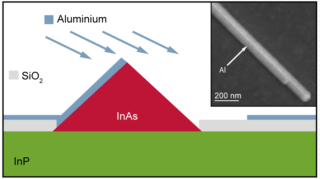
The fully developed cross-sectional equilibrium shape of the NWs allows for directional deposition of a superconductor (or other materials) on selected facets of the NWs, see illustration in Fig. 1. In hybrid semiconductor-superconductor devices, this is an advantageous geometry as it allows for tuning of the carrier density with side/top gates. Full shell devices are difficult to gate with standard side-gate geometries, due to the superconductor electrostatic screening. In the inset of Fig. 1 we show an InAs NW with Al deposited from an angle of 33∘ from the wafer normal, this resulted in a uniformly coated facet, but in this particular case for [100] orientated NWs, it also results in deposition of an undesirable thin layer on the second NW facet. Regardless, the density in the NW could still be tuned with a side gate, because the thin dewetted layer oxidizes as it is taken out of the growth chamber.
.2 S2. Substrate fabrication
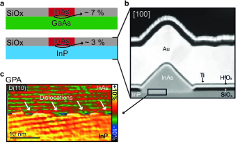
Semi-insulating Fe-doped InP and undoped GaAs (001) substrates are utilized because of their compatibility with as-grown device fabrication and measurements at low temperatures. First 10-30 nm of SiOx or SiNx is grown by plasma-enhanced chemical vapour deposition (PECVD) on the epi-ready wafers. Mask openings were defined by standard electron beam lithography (EBL). For the SiOx mask a short acid dip (3 s in buffered hydro-fluoride, BHF) is used to strip the oxide in the defined polymer windows. For SiNx masks reactive ion etching was used to create the mask opening.
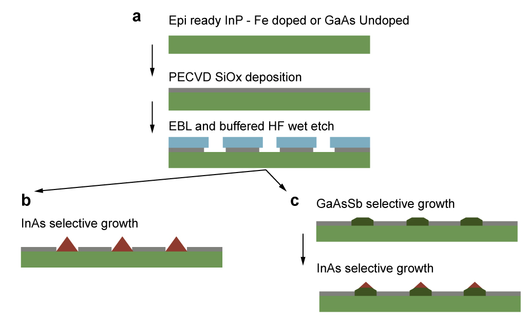
After thorough cleaning in ultra-pure milli-q water, and iso-propanol and acetone, the samples are subjected to O2 plasma ashing before the wafer is loaded into the MBE system and degassed in UHV at 250 ∘C (for InP) or 350 ∘C (for GaAs) for two hours before entering the growth system. See Fig. 2 for illustration of fabrication principle.
.3 S3. Non-buffered InAs SAG on GaAs (001) substrates
.4 S4. AFM of [110]/[1-10] junction
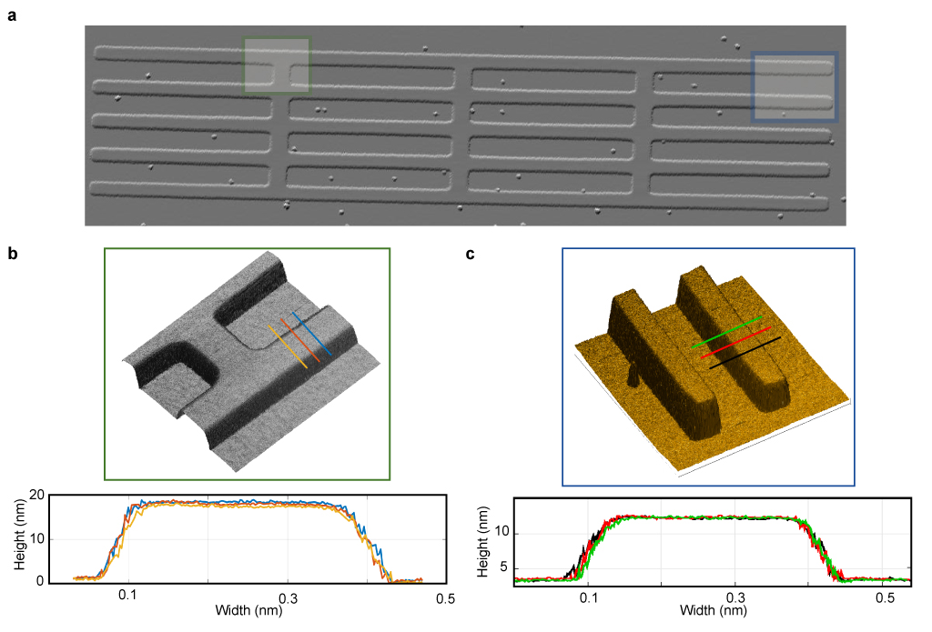
Here we investigate the flatness of the [100] top facet of the GaAs(Sb) buffer in order to see whether the orientation of the grown buffer has an impact on the flatness. The GaAs(Sb) buffer layer was investigated by atomic force microscopy (AFM) imaging of the [110]/[1-10] networks (as opposed to the [100]/[010] junctions in the main text). We find that the roughness of the [110]/[1-10] junction is comparatively similar to the [100]/[010] junction roughness, as shown in Fig. 4.
.5 S5. InAs nanowire grown on top facet - with width smaller than the mask width
One of the advantages of selectively growing NWs on a buffer layer is that it allows for reducing the NW diameter below the width of the mask opening, as shown in Fig. 5.
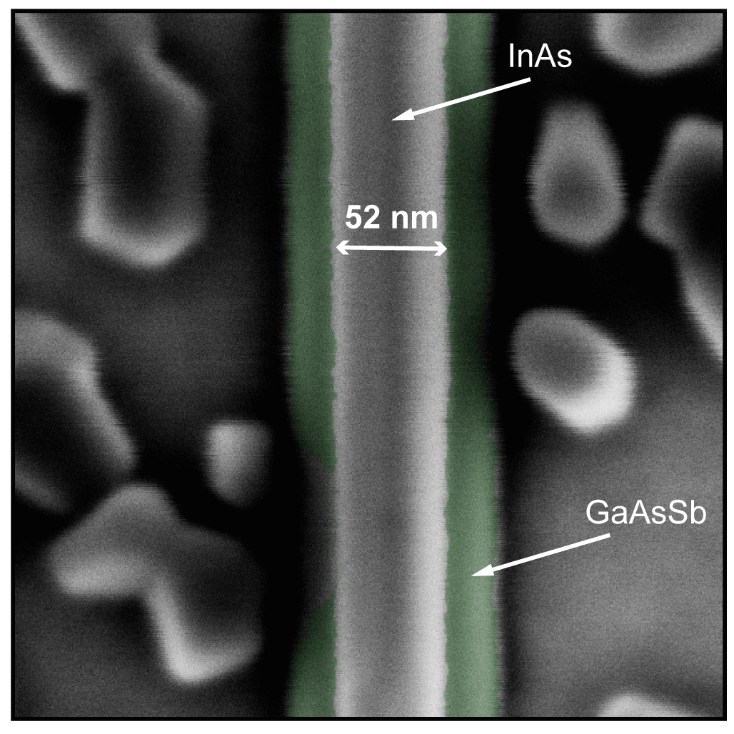
Growth solely on the top facet is seen for thin layers, as also reported on GaSb buffers in Ref. [(1)]. Additionally, this approach is advantageous because the transport channel is not in direct contact with neither the processed substrate surface nor the oxide mask, especially since fabrication of mask openings with atomically smooth sidewalls is challenging.
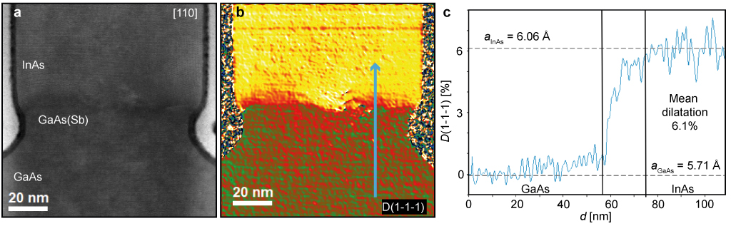
.6 S6. Non-buffered interface to substrate
The NWs were grown directly on GaAs (7 % strain) and InP (3 % strain) substrates, as sketched in Fig. 6 a. The devices used for transport measurements in the main text are sliced into thin lamellae using a focused ion beam (FIB) on the top gate structures, for more details see Methods. The samples are investigated by atomic-resolution aberration-corrected high-angle-annular-dark-field scanning transmission electron microscopy (STEM) as seen in Fig. 6 b.
The HfOx is used as a dielectric before evaporating Ti and Au to form the top gate. On top of the whole structure a thick layer of Pt is deposited to protect the structure from Ga implementation and amorphization during the FIB process.
Geometrical phase analysis (GPA) is performed on the interface between the InAs and InP where the two structure are fully in-elastically relaxed at the interface, as indicated by the presence of misfit dislocations running parallel to the interface in Fig. 6 c. The GPA of the dilatation of the [110] oriented NW in Fig. 7 a and b shows that the lattice constant fully relaxes from GaAs to InAs across the 20 nm buffer-region.
.7 S7. Hysteresis on buffered and non-buffered NW devices
In Fig. 8 we show examples of conductivity, , traces as a function of the gate voltage, g, for a non-buffered and a buffered device. Here the “non-buffered” refers to an InAs NW grown directly on InP substrate while the buffered to InAs NW grown on a GaAs(Sb) buffer on a GaAs substrate. The growth of the InAs transport channel on top of the GaAs(Sb) buffer layer significantly improves the carrier density tuning and hysteresis. This improvement was apparent regardless of the NW orientation or dimensions.
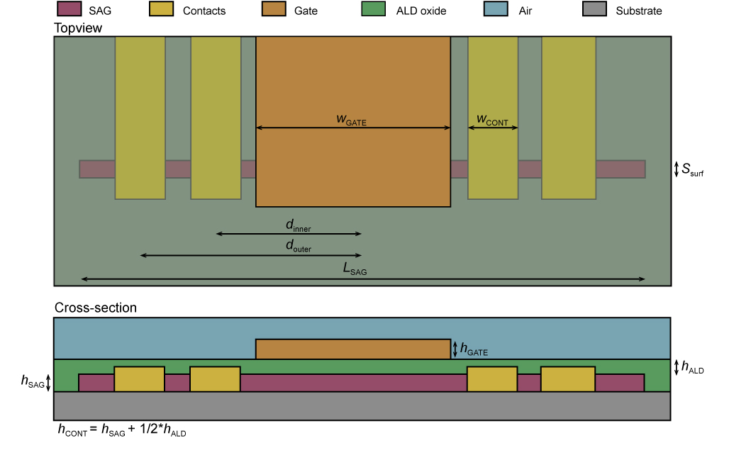
.8 S8. Finite element method capacitance modeling
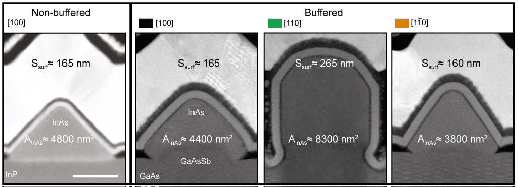
The device capacitances were simulated using the finite element method in the electrostatic module in COMSOL Multiphysics. Figure 9 summarizes the geometrical input parameters of the model, where the exact values were extracted from SEM images of the devices and geometrical cross-sections as shown in Fig. 10. The geometry of the NW was approximated by a rectangular cross-section with the width corresponding to surf as also shown in Fig. 9.

Two additional approximations were that the height of the gold contacts is set as CONT = SAG ALD and that the real height of the atomic layer deposition (ALD) oxide layer ALD corresponds to reality between the NW and the top-gate, but elsewhere it is given as = SAGALD. Another parameter is the effective dielectric constant of the used HfOx in combination with the NW native oxide, which was estimated as = 6.5.
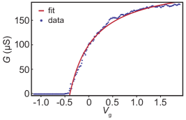
.9 S9. Field effect mobility fit
The field effect mobility is extracted for the buffered devices by fitting the equation from Ref. [(2)],
to the pinch-off curves measured at temperatures on the order of 5 K, as shown in Fig. 11. Here is the conductance, is the length of the InAs channel and , and probe resistance are the fit parameters. The is found from the finite element modeling described in S8.
.10 S10. Aharonov Bohm oscillations and frequency extraction
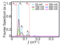
The Fourier transform of the data in Fig. 5 from the main text, showing the normalized amplitude of the / oscillations. The largest amplitude denoted, , corresponds to the / oscillation. The higher frequency peaks, corresponding to and , could be attributed to two things: (1) The asymmetric cross-section of the InAs NWs grown on the GaAs(Sb) buffer as seen in Fig. 5 in the main text, results in more than one effective circumference and thus contain multiple available transport paths. (2) Electronic waves propagating around the loop more than once results in higher order harmonics. The two dashed lines corresponding to out and in mark the outer and inner areas of the loop. Since the higher harmonics are not residing at double the frequency of and all amplitudes are within the area bound out and in explanation (1) is more probable.
References
- Fahed et al. (2016) M. Fahed, L. Desplanque, D. Troadec, G. Patriarche, and X. Wallart, Nanotechnology 27, 505301 (2016).
- Gül et al. (2015) Ö. Gül, D. J. Van Woerkom, I. van Weperen, D. Car, S. R. Plissard, E. P. Bakkers, and L. P. Kouwenhoven, Nanotechnology 26, 215202 (2015).