Towards a Simple, and Yet Accurate, Transistor Equivalent Circuit and
Its Application
to the Analysis and Design of Discrete and Integrated Electronic Circuits
Abstract
Transistors are the cornerstone of modern electronics. Yet, their relatively complex characteristics, allied with often observed great parameter variation, remain a challenge for discrete and integrated electronics. Much of transistor research and applications have relied on transistor models, as well as respective equivalent circuits, to be employed for circuit analysis and simulations. Here, a simple and yet accurate transistor equivalent circuit is derived, based on the Early effect, which involves only the voltage and a companion parameter . Equations are obtained for currents and voltages in a common-emitter circuit, allowing the derivation of respective gain functions. These functions are found to exhibit interesting mathematical structure, with gain values varying almost linearly with the base current, allowing the gains to be well characterized in terms of their average and variation values. These results are applied to deriving a prototypic Early space summarizing the characteristics of transistors, enriched with recently experimentally obtained prototypes of NPN and PNP silicon BJTs and alloy germanium transistors. Though a trade-off between gain and linearity is revealed, a band characterized by small values of stands out when aiming at both high gain and low distortion. The Early equivalent model was used also for studying the stability of circuits under voltage supply oscillations, as well as parallel combinations of transistors. In the former case, it was verified that more traditional approaches assuming constant current gain can yield stability factors that deviate substantially from those derived for the more accurate Early approach. The equivalent circuit obtained for parallel combinations of transistors was shown also to closely follow the Early formulation.
“Where there is matter, there is geometry.”
J. Kepler
I Introduction
Developed in 1947 riordan:1997 , transistors quickly became the cornerstone of modern electronics. Because of their central importance, be it in integrated or discrete circuits, these devices have become the subject of intense and continued research from both theoretical (e.g. semiconductor physics) and practical (e.g. electronic engineering) points of view. There are two main applications of transistors: digital and analog (e.g. jaeger:1997 ; sedra:1998 ; boylestad:2008 ; horowitz:2015 ; streetman:2016 ). In the former case, transistors are used as switches transitioning between two logical levels, which underlies the area of digital electronics. In the latter case, transistors are typically used as linear amplifiers, characterizing the area known as analog (or linear) electronics (e.g. pettit:1961 ; hyat:1962 ; analogdesign:1988 ; analogdesign:1991 ; casier:2011 ; carusone:2012 ; sedra:1998 ). Because the many signals in nature exhibit continuous values, being therefore called analog, linear electronics continues to be essential for myriad electronic applications. Here, the challenge is to achieve efficient circuits capable of amplifying signals with the lowest level of distortion. This constitutes a challenging endeavor because transistors are inherently non-linear devices. So, at least three alternative approaches have been typically considered in order to try obtaining linear amplifiers by using transistors: (i) to improve the of the devices; (ii) to find the most linear operation region; and (iii) to develop circuits capable of enhancing linearity. With the introduction of negative feedback in electronics by H. S. Black in 1927 black:1934 , alternative (iii) became the most standard and commonly applied approach for achieving practical amplifying circuits with improved linearity.
All the above mentioned three approaches to enhance linearity when using transistors share a common, critical aspect: they all rely critically on the availability of effective transistor models, representations and equivalent circuits. As a consequence, several modeling and equivalent circuits have been proposed and used in linear electronics (e.g. pettit:1961 ; hyat:1962 ; analogdesign:1988 ; analogdesign:1991 ; jaeger:1997 ; casier:2011 ; carusone:2012 ; streetman:2016 ). An alternative transistor modeling approach was reported recently costaearly:2017 ; costaearly:2018 that relies on the Early effect, discovered by J. M. Early in 1952 early:1952 ; ziel:1968 ; streetman:2016 . This effect is characterized by the variation of the charge carrier portion of the base with the base-collector voltage. An immediate consequence of this phenomenon in junction transistors is that the characteristic isolines of transistors (indexed by the base current) will not cross the collector voltage axis at , but at a further away negative value , which corresponds to the Early voltage. Though these facts have been known for a long time, they have not often considered for modeling transistors, except for a few works relating the Early voltage with the transistor output resistance , especially in the case of FET devices (e.g. AD:2017 ).
The methodology described in costaearly:2017 ; costaearly:2018 uses the Early effect to derive a complete transistor model characterized by two parameters: the Early voltage and a proportionality parameter relating the characteristic isoline angles with the modulating base current . Perhaps the key element in this alternative type of transistor modeling consists in the fact that it was experimentally found for hundreds of small signal BJTs costaearly:2017 ; costaearly:2018 ; germanium:2018 that , i.e. the isoline angles are directly proportional to the base current. This linear relationship not only simplifies the Early modeling approach, but also leads to the specially important property that both the parameters involved in the Early model result completely independent of the transistor/circuit operation in the space . This contrasts sharply with the fact that in the more traditionally applied models, the two involved parameters current gain and output resistance vary with the normal operation of the circuit. This has implied that, given a specific transistor, it is impossible to characterize it by a single parameter setting , being necessary to consider maximum or average values of these parameters along the operation space, which is not accurate because the parameters of the transistor characteristic isolines tend to vary extensively even in normal operation. It should be recalled that several other transistor models have been employed (e.g. gray:1969 ; sedra:1998 ; boylestad:2008 ; streetman:2016 ), some of which aimed at providing more complete representations by incorporating a larger number of components.
In spite of its recent introduction, the Early modeling approach costaearly:2017 ; costaearly:2018 has already been successfully applied to several issues in electronics, including the characterization of real-world NPN and PNP silicon costaearly:2017 and germanium germanium:2018 junction devices, allowing the derivation of a prototypical atlas of device characteristics in which NPN exhibit lower parameter variations than the PNP counterparts. In addition, it was found that both the NPN and PNP transistors tended to have the same average while differing markedly in and values, parameters that had not been usually considered. It has also been verified that the total harmonic distortion of transistors depends only on the parameter , being independent of the Early voltage . Actually, the intrinsic adherence of the Early model to the geometrical structure of transistors, allied with the simplicity and accuracy of the proposed basic mathematical representation, paves the way to several advances in understanding, designing, and applying transistors in integrated (e.g. gray:1990 ; carusone:2012 ) and discrete circuits. The geometry of device operation constitutes a particularly promising perspective because not only it promotes better and more intuitive understanding of the potential behavior of a device (often in a very complete way), but it also provides the scaffolding for deriving more effective and intuitive mathematical representations, models, and respective equivalent circuits. Indeed, graphical approaches have been extensively used since the beginnings of electronics, and many of the textbooks from 50’s to 70’s (e.g. shea:1955 ; zimmermann:1959 ; pettit:1961 ; fontaine:1963 ; alley:1966 ; gronner:1970 ; tinnell:1972 ) are characterized by extensive and systematic use of graphical presentations and developments. Perhaps the progressive shift to numeric-computational modeling of device operation along the 70’s and 80’s has shifted a little bit this paradigm, but graphical approaches remain, nevertheless, an interesting resource to be considered, exhibiting potential for enhancing the available simulation resources. So, its is not that graphic representations of device operation should be replaced by numeric-computational simulation approaches, but that it should be incorporated as a valuable and useful concept that could contribute to advances in simulation approaches.
By having access to effective transistor models, devices operating in the so-called “linear” regime and having forward-biased base-emitter junction and inversely-biased base-collector junctions can be conveniently substituted by their respective equivalent circuits, providing a better understanding of the circuit characteristics and promoting possibilities for further enhancements. The derivation of transistor equivalent circuits can benefit greatly from the Early model costaearly:2017 ; costaearly:2018 intrinsic simple geometry fully compatible with transistor operation, characterized by radiating isolines. The main objective of the current work is to develop such an equivalent circuit for the Early model of transistors, and illustrate its theoretical and practical application potentials with respect to the characterization of important electronic properties of transistor-based circuits, including current, voltage and power gains as well as distortion. In addition, the proposed equivalent model is also applied to the analyses stability of circuits in presence of power supply oscillations and parallel combinations of BJTs.
This article starts by revising a more traditional transistor modeling approaches based on the current gain and output resistance , and proceeds by presenting the Early modeling approach and deriving respective equivalent circuits, from which current and voltage equations describing the behavior of a simplified common-emitter circuit configuration are derived. These equations are then employed to quantify respective current and voltage gains, exhibiting an interesting mathematical structure that implies that, at least for the considered circuit and parameter configurations, the gains vary in very nearly to linear fashion with the modulating current base . This fact allows the gains to be effectively quantified in terms of their respective average and variation values. These results allowed the derivation of a prototypic Early space characterizing a trade-off between gain and linearity, as well as incorporating prototypic groups of NPN and PNP silicon and germanium devices. The potential of the Early equivalent circuit is further illustrated with respect to applications to the study of stability induced by voltage supply oscillations as well as for the characterization of parallel combinatios of transistors.
II Real-World Transistor Characteristic Surfaces
Real-world transistors are characterized by several specific features regarding their electronic behavior, and these features tend to vary from one device to another. Figure 1 illustrates the characteristic surface, represented in terms of its constituting isolines, each one indexed by a respective base current , of a real-world PNP small signal transistor. This characteristic surface was obtained experimentally by using a microprocessed acquisition system costaearly:2017 ; costaearly:2018 . The operation space corresponds to the Cartesian coordinate system , where is the voltage current measured with reference to the ground and is the collector current (positive sign corresponding to current entering the device). The characteristic surface in this figure was obtained for the operation region defined by , , and . The transistor was set in a simplified common emitter configuration alley:1966 ; gray:1969 ; thomson:1976 ; horowitz:2015 , with inversely biased base-collector junction and forward-biased base-emitter junction, with a resistive load attached between the collector and the external voltage source . For simplicity’s sake, all current and voltage values of PNP transistors are represented by inverse values, so as to keep the operation space in the first quadrant, therefore achieving a unified approach with respect to NPN devices.
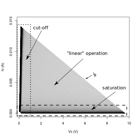
Interestingly, characteristic surfaces such as that shown in Figure 1 incorporate all information necessary to characterize the operation of the respective device, except in cases where it has reactive components. The most important region of the characteristic surface is that where the indexed isolines tend to be straight and reasonably spaced one another. This region is often called the “linear” operation region. The narrow vertical region next to the axis corresponds to the transistor saturation and are normally avoided during linear transistor operation. Similarly, the narrow horizontal strip next to the axis, often called the transistor cut-off region, is characterized by coalescence of isolines and is similarly not taken into account for linear transistor operation.
The isolines in the linear region are mostly straight lines with slopes that increase with . Recall that the slopes of these isolines correspond to , where is the output resistance of the collector. Observe also that the isolines bend at the cut-off region, but are very nearly straight otherwise. NPN transistors have similar characteristic surfaces, except for the fact that the isolines tend to have smaller slope costaearly:2018 . Because the characteristic surfaces of real-world transistors are somewhat complicated, simplified versions are typically adopted for obtaining mathematical characterization of the transistor behavior, as well as respective equivalent circuits. A traditional approach to modeling the characteristic surface, as well as the respectively derived equivalent circuit, is revised in the next section.
III A Traditional Approach to Transistor Modeling
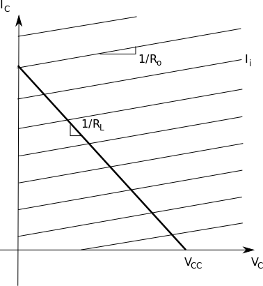
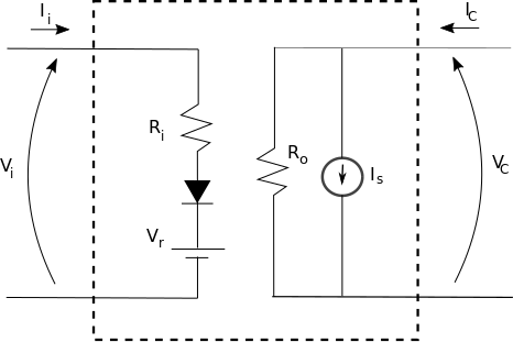
Figure 2 shows a simple NPN transistor characteristic surface in the circuit operation space, in which all the equispaced -indexed isolines are assumed to have the same slope , therefore being parallel one another. This configuration is normally used assuming that the base-collector junction is reversely biased while the base-emitter junction is forward biased, hence the input port can be approximated by a simplified diode model as in this figure, where stands for its internal resistance (observe that the ideal diode in this figure can be omitted under the above hypotheses).
Though it is know that, for most real-world transistors, the slopes actually increase with , this fact is not considered in this model for simplicity’s sake. As a matter of fact, an even simpler transistor characteristic is sometimes used in which all equispace isolines have null inclination, implying . Despite these simplifications, such approaches remain interesting, as they provide insights about how more idealized transistors would behave, and can also be used in introductory didactic syllabuses.
In this section, we review the analysis of the electronic properties of the ideal transistor represented by the characteristic surface in Figure 2. First, we obtain the current and voltage equations for the input and output ports, and then use these equations in order to derive the current, voltage and power gain, and discuss linearity.
The simplified characteristic surface in Figure 2, together with the assumed simplified diode model, yields the equivalent circuit shown in Figure 3. The ideal diode is included for the generality’s sake, but can be omitted under the adopted transistor base-emitter forward bias. Observe that the -indexed isolines are obtained by incorporating the constant current source in parallel with an internal output resistance (Norton equivalent).
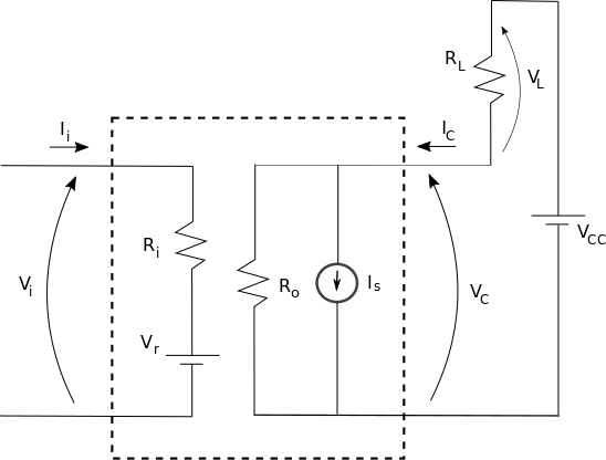
We consider a simplified common emitter circuit configuration as in Figure 4. Here, a load resistance is attached between the external voltage source and the transistor output (collector). It can be easily verified that this pair of components external to the transistor define a straight line in the space as in Figure 2. This line is commonly called load line. The circuit operation is now restricted to take values along this load line. While the resistance corresponds to the actual load of the transistor, the voltage source is required because the transistor, being a passive device, can not deliver power into the load, but only control an external voltage or current source according to the input current . That is why transistors operating as amplifiers are sometimes called “valves”.
First, we approach the base-emitter junction, which we assumed to operate as a simplified diode. For this input port, we have:
| (1) |
Now, we proceed to the output port. By defining the transistor current gain and applying Kirchhoff’s and Ohm’s laws (e.g. hyat:1962 ), we have that:
| (2) | |||
| (3) | |||
| (4) |
When , the transistor output stage becomes a perfect current source and we have:
| (5) | |||
| (6) | |||
| (7) |
The AC current, voltage and power gains at the resistance load are commonly defined, respectively, as:
| (8) | |||
| (9) | |||
| (10) |
Strictly speaking, the AC gains are defined respectively to an operating point . This effectively implies . In addition, because of the constant slope of the -indexed isolines in the simplified transistor model under consideration, the choice of this point becomes immaterial and we have:
| (11) | |||
| (12) | |||
| (13) |
So, we have that all the considered gains do not depend on , or , as would be expected as a consequence of adopting equispaced isolines. For the further simplified case when , we have:
| (14) | |||
| (15) | |||
| (16) |
IV The Early Model Approach
Now, we revisit the circuit configuration discussed in the previous section, but adopting a simple Early model costaearly:2017 ; costaearly:2018 instead of the just considered current-source model. Figure 5 depicts the characteristic surface underlying the adopted Early model, defined in terms of a set of -indexed isolines radiating from the same point along the axis. Observe the varying inclination and spacing of the -indexed characteristic isolines along the load line, which account for a more accurate and realistic representation of the transistor intrinsic electronic properties, as can be immediately inferred by comparing the diagram in Figure 5 with the experimental characteristic isolines of the real-world transistor in Figure 1.
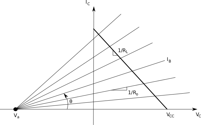
Though the “fan”-like radiation may initially appear as a complication, it will turn out that this is not really so. In addition, this geometrical organization provides a much more accurate representation of the behavior or real-world transistors than the previous simplified approach, as it allows the increasing slopes of the non-equally spaced isolines to be taken into account costaearly:2017 ; costaearly:2018 . Observe that these slopes correspond to the inverse of the output resistance , and also that . In addition, the two parameters involved in the Early modeling, namely the Early voltage and the proportionality parameter , remain constant throughout the operation space, i.e. these two parameters do not depend on either or (which is not verified for more traditional approaches based on and ). These key properties of the Early approach, that constitute the main motivation of the present work, are summarized in the following box:
In the Early model, the characteristic surface of real-world transistors, allowing for varying slope of non-equally spaced characteristic isolines indexed by the base current , is represented in terms of only two constant parameters ( and ) that provide a very comprehensive characterization of the device operation.
The possible reason why such an Early model approach costaearly:2017 ; costaearly:2018 was been adopted earlier is because the relationship between and did not seem to be known. However, at least for several types of small signal transistors, it has been experimentally verified recently costaearly:2017 ; costaearly:2018 that , allowing a substantially simple and effective transistor model to be developed and applied costaearly:2017 ; costaearly:2018 . Therefore, only two elements underly the Early model: the hypotheses that , and the fact that the all the -indexed isolines intersect at a same value along the axis. The Early model is immediately applicable equally to NPN and PNP models, and in this work all PNP currents and voltages are shown with negative values, for simplicity’s sake.
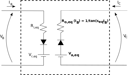
The equivalent circuit of the graphical construction shown in Figure 5 can now be easily derived as illustrated in Figure 6. The input port is modeled in the same way as in the previous section. However, in the Early approach, the output port of a transistor is now represented as voltage source with fixed value corresponding to the Early voltage, in series with a variable output resistance , where is the proportionality constant constituting the second parameter in the Early model costaearly:2017 ; costaearly:2018 . Rarely, if ever, equivalent circuits employ variable resistances (or conductances), but there is no intrinsic shortcoming in this type of approach. On the contrary, the -controlled resistance of the isolines provides a natural represented by the geometrical organization of the transistor operation. Observe also that though a respective Norton version of the equivalent circuit proposed for the Early modeling would be possible, it would imply both output resistance and current source to vary with , while the voltage source in the adopted Thevenin configuration remains constant with as well as with and .
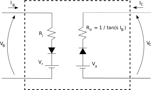
The presented Early equivalent circuit can be understood as having similar complexity to the varying current source model in Figure 3. However, it is typically much more accurate than that model as allowed by the variable resistance representation of the progressively more inclined, non equally space isolines found in most real-world transistors. It could also be argued that the voltage-based (Thevenin) approach is probably more intuitive than the more traditional current-based (Norton) counterpart.
Figure 7 shows the same circuit as in the previous section, but with the transistor represented in terms of its Early model. Since the base-emitter is forward biased and the base-collector is inversely biased, the two diodes can be conveniently omitted.
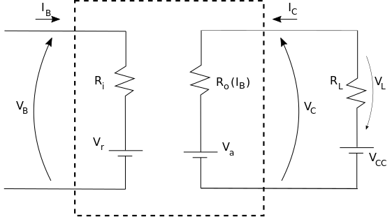
Because the input port is modeled in the same ways as in the previous section, Equation 1 is verified also for this circuit configuration. The output current, as well as and at the output stage can be immediately determined by applying Kirchhoff and Ohm’s laws as:
| (17) | |||
| (18) | |||
| (19) |
where . These expressions are hardly more complicated than those obtained for the more traditional, and less precise, modeling approached addressed in the previous section.
The current, voltage and power gain are now given as:
| (20) | |||
| (21) |
Though this last pair of equations is slightly more sophisticated than those obtained for the more traditional modeling approach discussed in the previous section, this is so because now they account for the important fact that all gains are indeed functions of . This is particularly important because this dependence directly implies that the current, voltage and power amplifications will necessarily be non-linear in a real-world circuit employing a real-world transistor.
The AC version of the obtained current and voltage gains (the power gain will be henceforth omitted as it can be directly obtained as ) can now be calculated as:
| (22) | |||
| (23) |
It is interesting to rewrite the above equations as:
| (24) | |||
| (25) |
so that we can now define the two functions and that play the role of kernels of the transistor operation:
| (26) | |||
| (27) |
These functions are critically important because they define the linearity of the transistor amplification in the considered circuit configuration. Both and depend only of the base current , the proportionality parameter , and the load resistance . The current and voltage gains can be easily obtained by multiplying and by and , respectively, as implied by Equations 43 and 44.
Figure 8 illustrates the behavior of in terms of , and Figure 9 depicts the function in terms of these same two variables for and . For simplicity’s sake, we henceforth set and , which is typical of small signal real-world NPN devices costaearly:2018 . Both cases assume and , but similar behaviors are observed for other typical parameter value configurations.
For any fixed , decreases with in an almost linear fashion, especially for smaller values of . Similarly, also decreases with for fixed (except for , when ), but now in an almost perfectly linear fashion. Indeed, the relative variations of and with both increase with the fixed value.
Given the almost linear variations of and , they can be effectively characterized in terms of their average and variation values. The former of these are immediately given as:
| (28) | |||
| (29) |
The gain variations are all important for characterizing the linearity of the transistor operation (observe that increased variations will imply larger distortions in the amplification), so that it is worth defining them in terms of the relative maximum excursions, i.e.:
| (30) | |||
| (31) |
where and are immediately calculated by using Equations 26 and 27, respectively. Interestingly, these variations are directly related to the total distortion implied by the respective amplifications. In particular, full linear operation would be achieved if the variations were null.
The nearly linear variations of the current and voltage gain with indicate that, at least for the considered parameters and variable ranges, the properties of those gains can be effectively quantified in terms of the respective average and variation values.
We are now in a position to study the overall AC properties of the considered transistor/circuit configuration – namely the current and voltage gains, as well as the overall implied distortions – in terms of all possible choices of the involved parameters, i.e. , , and . We limit our discussion to the current gain because an analogue behavior is observed for the voltage gain. Figure 10 illustrates the average current gain, obtained by multiplying by .
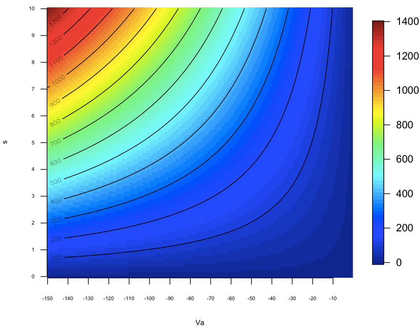
The average current gains tend to reach a peak at the top lefthand side of the Early space and the lowest values near the and axes. Respective isolines, indexed by the average current gain, are also depicted in this figure. They present progressively varying shapes, with curvature increasing towards the coordinate system origin. Observe that the average current gain increases in a non-linear fashion throughout the Early space, being characterized by steeper variations near the top lefthand side of the represented space.
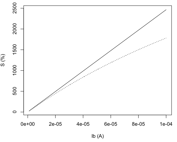
Figure 11 shows the absolute variation of the current gain along the considered portion of the Early space for and . The obtained pattern is similar to that exhibited by the average current gain, but it is less symmetrical along the horizontal and vertical orientations. The respective current gain variation isolines are also shown in this figure.
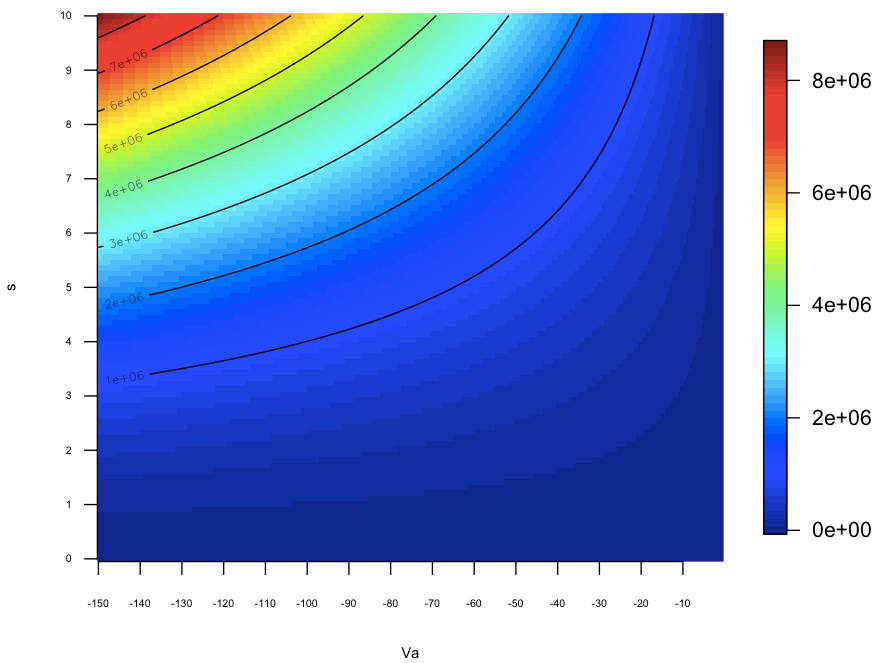
Enhanced linearity is achieved for the configurations near the or axes. Observe that the variation values are high because the variation is normalized by the interval, which is equal to . Another way to quantify non-linearity as related to the current gain variations is by considering relative instead of absolute values. This type of quantification is adopted henceforth in this work. Figure 12 depicts the relative current gain variations, obtained by dividing the previous variations by the respective average current gain.
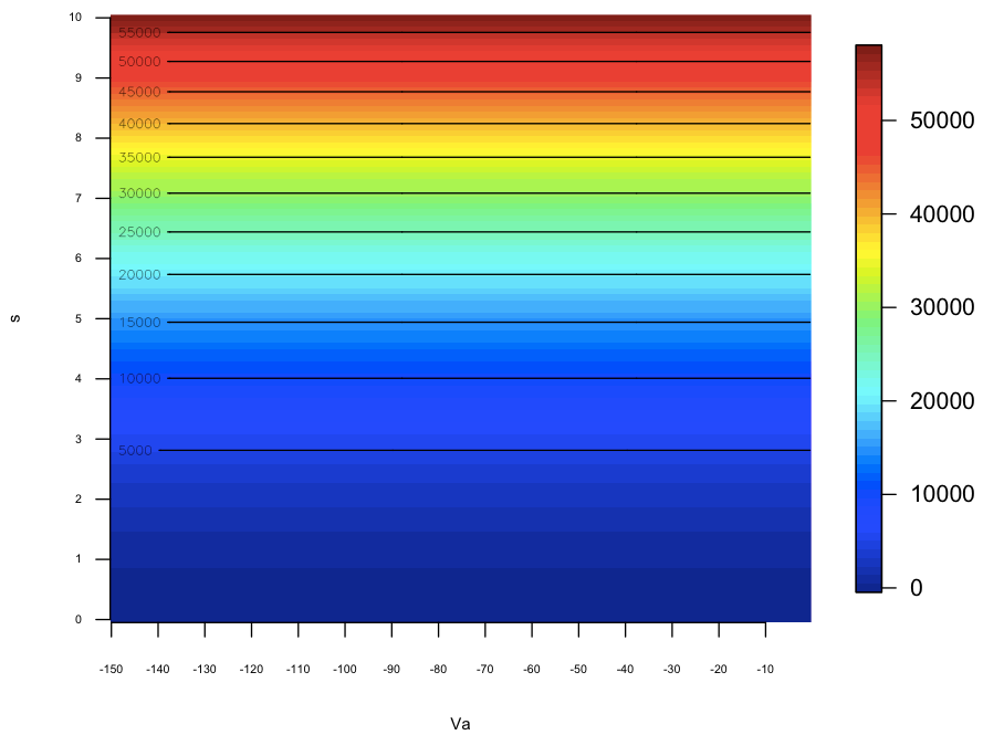
This remarkable result, already hinted by previous total harmonic distortion considerations in a previous work costaearly:2018 , indicates that the linearity of the transistor in the adopted circuit depends only of the values, being completely independent of the values. Therefore, horizontal isolines are obtained in the figure. Observe that the isolines spacing decreases progressively with . The most non-linear amplification is obtained for large values of , irrespectively of . Interestingly, a (welcomed) substantially wide band of low variation is observed near the axis.
The results revealed by the average current gain and its variations can now be neatly combined into a same diagram, henceforth called the prototypic Early space, to provide an overall representation of the trade-off between current gain and linearity in the considered circuit. Figure 13 shows the so obtained prototypic space, as well as Mahalanobis ellipses obtained experimentally for several NPN and NPN silicon costaearly:2018 and germanium germanium:2018 junction transistors. The isolines for (dashed line) as well as for (dotted line) are also shown in the figure, passing very near to the centers of mass (averages) of the considered groups of transistors.
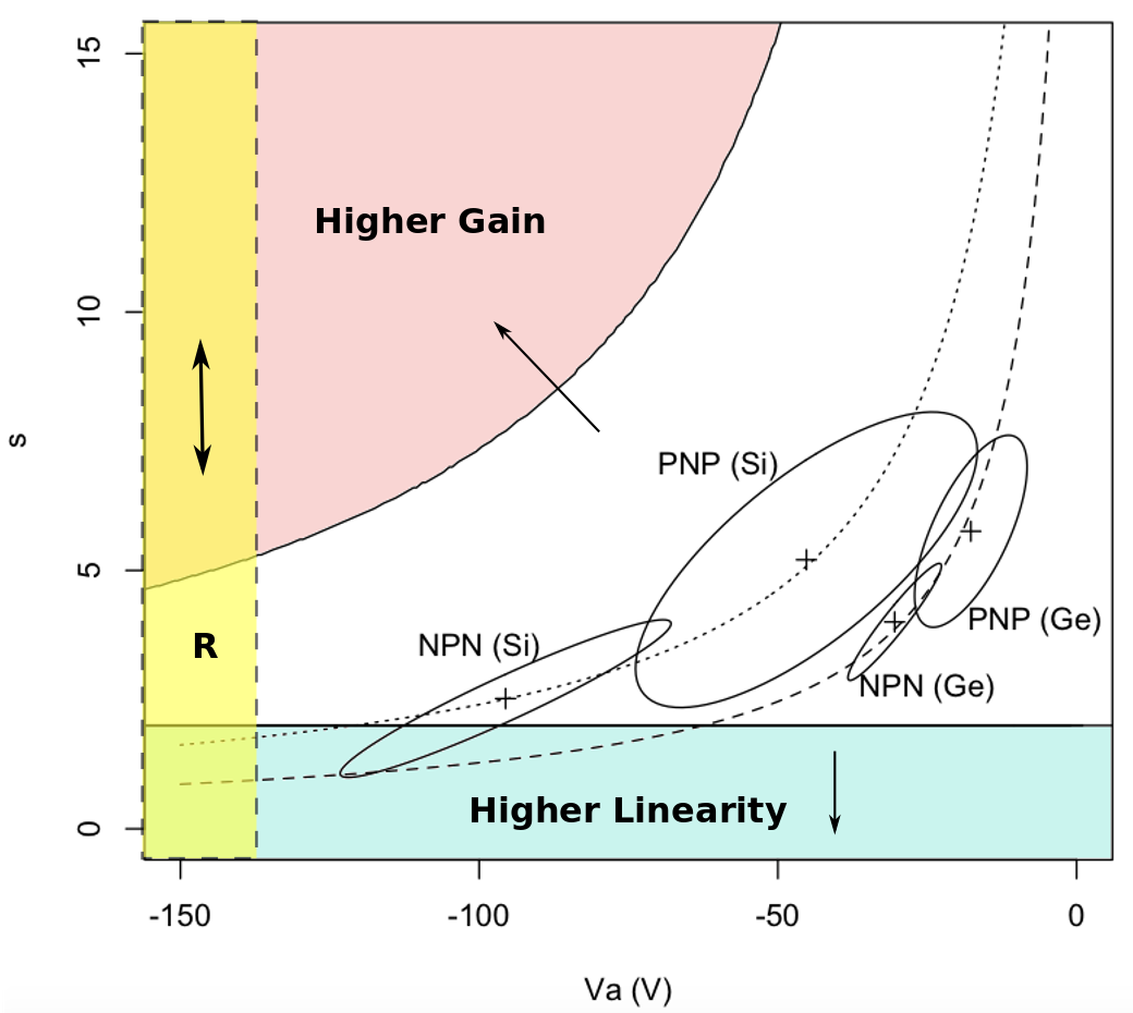
This prototypic space summarizes several key information about transistor operation, providing valuable subsidies for choice, applications, and design of transistors. If priority is placed on gain, devices near the red region should be chosen. Contrariwise, in case linearity is the main objective, devices near the green band should be considered. Now, it becomes evident that the high gain and high linearity tend to follow contrary pathways along the prototypic space, implying a trade-off between these two often sought characteristics. However, the different geometry of the average current gain and variation surfaces imply some regions of special interest when trying to optimize both gain and linearity. Though, in principle, the linearity does not depend of , if a large magnitude value of is chosen, such as in the yellow band in the figure, higher gain values can be obtained even when choosing transistors with smaller values of . In this way, the yellow region stands as having particular interest when aiming simultaneously at hight gain and good linearity. Also, observe the higher gain isolines tend to approach the axis for large magnitude values of that parameter, the implied funneling effect also implies lower values of and improved linearity. Thus, devices with very large are particularly interesting for providing a good combination of high gain and low distortion.
Interestingly, real-world NPN and PNP transistors, at least for the cases experimentally characterized costaearly:2018 , tend to occupy an intermediate position in the Early parameter space. The silicon NPN devices are those nearer to the yellow band, representing good candidates when aiming at both high gain and low distortion levels.
V Stability Factor Analysis
An important property of transistor-based amplifying circuits regards their stability (e.g. tinnell:1972 ) with respect to the current or voltage supply oscillations. Let’s obtain, by using the Early equivalent circuit, the current and voltage stability for oscillations of the circuit considered in the previous sections. This can be done as follows with respect to the collector current and voltage instability with respect to oscillations:
| (32) | |||
| (33) |
It follows that:
| (34) | |||
| (35) |
The voltage instability is directly related to the current stability , so we focus on the former index. Figure 14 illustrates the behavior of in terms of assuming and . The and used in the more traditional approach in Section III were obtained by using the mapping between the Early and parameters developed in costaearly:2018 .
A substantial discrepancy can be observed between the instability curves obtained by using the Early (dashed lines) and more traditional approach (solid line), as these diverge markedly, specially for larger values of . Interestingly, the instability obtained by using the more accurate Early equivalent circuit is smaller than that yielded by using the more traditional model. This is a probable consequence of the fact that the varying slopes of the -indexed isolines, which is represented in the Early equivalent circuit but not the more traditional approach, compensate for the voltage supply oscillations through a kind of saturating effect. Thus, real-world devices may turn out to have potentially increased stability than that revealed by more traditional approaches based on the parameters.
This simple application of the Early equivalent circuit to the analysis of an important practical parameter in linear circuit design and application, namely the variation of the amplification as a consequence of power supply oscillations, revealed that substantial discrepancies in the quantified electronic behavior of the analyzed circuits can be produce when overlooking the more realistic variation of the -indexed isolines in real-world devices.
VI Parallel Transistor Configurations
A single transistor is capable of delivering a limited amount of current to the load, being subjected to maximum absolute ratings. A possible means for trying to increase the power provided by the output port of transistors is to combine them in parallel as illustrated in Figure 15.
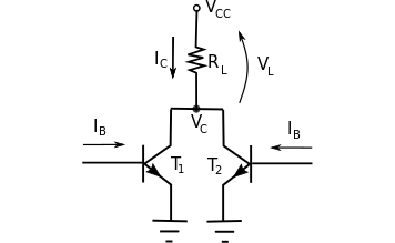
As illustrated in Figure 16, the Early equivalent circuit can be easily employed to analyze the parallel configuration of two transistors (the result can be immediately extended to more transistors).
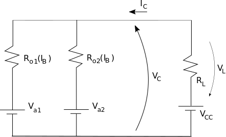
The so obtained circuit can now be analyzed by using Kirchhoff’s and Ohm’s laws, as well as the Thevenin equivalent theorem, to obtain the following equations of the resulting effective output resistance and Early voltage , both of which potentially dependent of :
| (36) | |||
| (37) |
For simplicity’s sake, and without loss of generality, we can make and . First, we have that:
| (38) |
and, consequently, it follows that:
| (39) | |||
| (40) |
Interestingly, turns out to be almost perfectly constant with for the parameters and variables typically found in the considered circuit configurations to the point that the variation often results smaller than double floating point precision. So, the equivalent transistor effectively has, effectively, a constant Early voltage determined only by , , and . This nearly constant value of can be conveniently obtained by applying L’Hospital theorem to Equation 40, which yields:
| (41) |
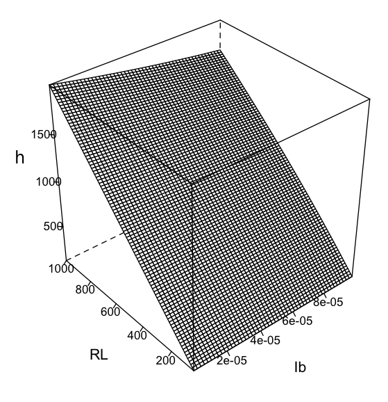
The dependence of with and is depicted in Figure 17.
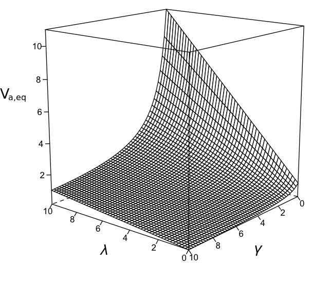
So, increasing promotes linear larger values of , and this increase is more accentuated for smaller values of . However, the effective can never exceed the maximum between the two original Early voltages and .
Another remarkable property of the parallel transistor combination is that the proportionality ratio and is also virtually invariant with . This means that the pairwise combination of transistors will have an equivalent output resistance that will not interfere with the degree of linearity of the resulting device. As a consequence, parallel combinations of transistors cannot imply in new types of characteristic surfaces deviating from the Early model geometry. Similarly, by applying L’Hospital theorem:
| (42) |
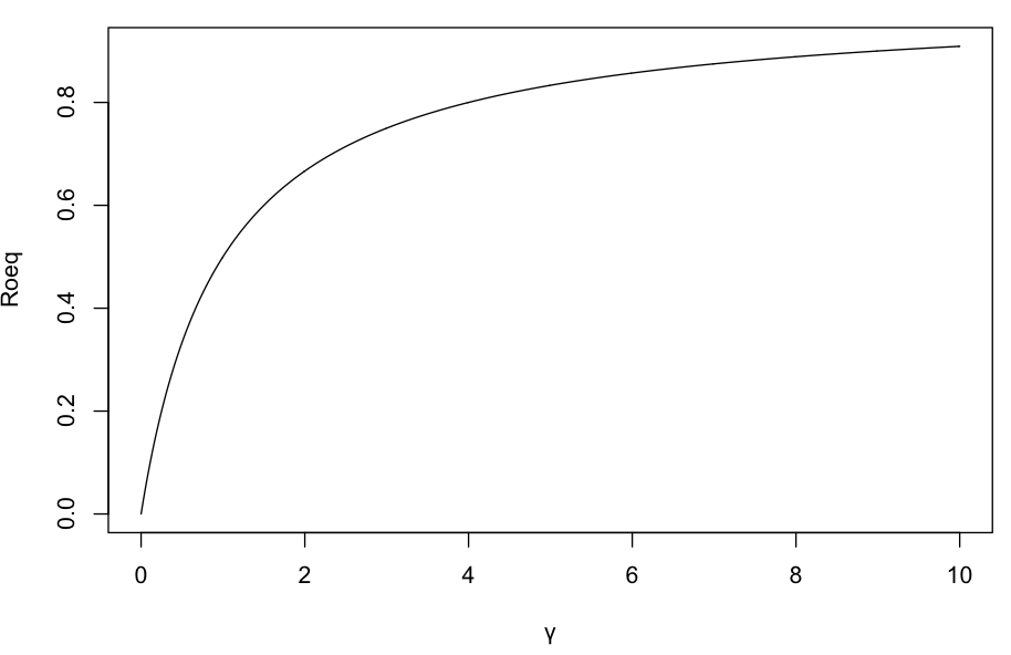
Figure 18 shows the range of that can be obtained by varying . Observe that the equivalent resistance tends to saturate at 1 for very large values of .
As the equivalent and initially seemed to depend on , this could lead to novel qualitative behavior of the parallel combination of transistors, such as eventual displacement of the point along the axis during normal circuit operation, or non-linear dependencies of with implied by not being constant with . However, the interesting obtained results imply that the parallel combination of transistors, at least for the considered configuration and parameters and variables ranges, will effectively result in a new transistor described by the same qualitative behavior as dictated by the Early equivalent circuit (see Figure 19). So, parallel combinations can be used to “design” new devices with parameters that are intermediate between the two original transistors. For instance, a transistor with smaller can be obtained by combining two transistors with larger values. Observe that the resulting and values will never be larger than the respective values of the original combined transistors.
VII Concluding Remarks
Transistors have been around since the mid 40’s, playing a decisive role for the development and popularization of modern electronics. Yet, their seemingly complex operation, which constrains the linearity of applications, has motivated much effort aimed at better understanding, modeling, applying and designing improved devices and circuits. There are two main vectors motivating the continued interest in transistors: (i) they are used in a vast range of applications underlying most of human activities, some of them critically; and (ii) oftentimes, transistors are required to operate with as much linearity as possible, which implies several challenges given the practical variability of transistor parameters allied to their relatively complex behavior. Originally, the focus of interest in transistor research was directed toward discrete devices and circuits, and great attention tended to be given to graphical representation and modeling approaches. With the introduction of integrated technology, interest shifted to transistors as the basic elements in integrated circuits, often studied by using numeric-computational simulations. However, several applications still justify, or even require (as in power electronics), the application of discrete devices. Be that as it may, discrete and integrated transistors follow the same physical constrains, so that they can be treated by the same unified approaches.
As a consequence of the continuing interest in transistor electronics, a vast quantity of works have been reported aimed at characterizing, modeling and design these devices. One of the main approaches consists in deriving, experimentally or from basic physical principles, the functional response of the devices (often done in a graphic way, with the help of transfer functions and other types of diagram), and then obtaining respective equivalent circuits that can be incorporated into circuit analysis performed analytically or through simulations. Several of the traditional transistor models are based on two parameters, the current gain and the (collector) output resistance . While these two parameters are particularly intuitive, as they are closely related to transistor electronic operation in circuits, they have an intrinsic limitation in the sense that they vary, often significantly, with normal circuit operation, taking different values for each current and voltage values taken by the transistor output.
A simple, and yet accurate, transistor model was developed recently costaearly:2017 ; costaearly:2018 founded on the Early effect, characterized by an interesting geometry of operation. In addition to the Early voltage sometimes used in transistor modeling, a second proportionality parameter is involved that governs how the angle of the base current-indexed transistor isolines vary with that current . Interestingly, this parameter has been experimentally found costaearly:2017 ; costaearly:2018 ; germanium:2018 to underly the simple linear relationship , at least for hundreds of small signal silicon and germanium BJTs, to vary in nearly full linear fashion. Therefore, both parameters and are fixed and constant for each given transistor, defining to a great extent its electronic properties. In addition, the mapping of transistors into the Early parametric space, instead of in more traditional spaces, has the advantage of allowing a better characterization and separation of different types of transistors costaearly:2018 ; germanium:2018 , possibly as a consequence of the fact that the Early approach captures directly the geometry of operation of real-world devices in the so-called “linear” operation region.
Despite having been introduced quite recently, the Early model has already been applied with encouraging success to several problems in electronics, including the estimation of transfer functions costaearly:2017 , the characterization of complementary BJTs including the derivation of a prototypic space costaearly:2018 , as well as the study of the electronic properties of alloy junction germanium transistors germanium:2018 .
In this work, an equivalent circuit is developed for the Early model in order to pave the way to its direct application in analysis and design of discrete and integrated circuits. We started by discussing the geometrical characteristics of real-world transistors, and then revised one of the simplified traditional models based on and , that have been largely used and applied in electronics. Next, the equivalent circuit of the Early model was derived, starting from characteristic surfaces with isolines radiating from a common point , corresponding to the Early voltage. The obtained circuit resulted substantially simple, with its output port including only a resistance and a voltage source connected in Thevenin series. However, this resistance turns out to be dependent on the base current , as well as on the Early parameters and , i.e. .
To illustrate the potential of this model, it was applied to the characterization of a simplified common emitter circuit configuration in which the load is directly attached between the transistor collector and the external voltage supply . The collector current, as well as the voltage across the load, were easy and conveniently derived by taking into account the Early equivalent circuit. Interestingly, these equations turned out to be no more complex than those obtained for the more traditional approach based on and , despite the fact that that the more traditional model considers a much more simplified situation in which the current gain does not vary during the transistor operation as a consequence of the equispaced parallel (though inclined) isolines. Then, equations for the DC and AC current, voltage and power gains were derived and, again, resulted not to be more elaborated than the respective counterparts obtained for the simpler, more traditional model.
The current and voltage gain equations (the power gain can be directly obtained from these to gains) were found to exhibit an interesting mathematical structure involving ratios between tangents. Two kernel functions and were derived, respectively, from these two gain equations. It is believed that these two equations are behind the intricacies of transistor operation. As illustrated graphically, the current and voltage gains vary in an almost perfectly linear fashion with , which suggests the derivation of the average and variation of the gains by taking into account only the extremities of the excursion of the gains as they vary with the same range of . This yielded two very simple expressions for quantifying the average current and voltage gains, as well as their variations, given the Early parameters and , the transistor input port resistance , as well as the circuit configuration (i.e. ). The gain variations are particularly interesting because they are directly related to the linearity of the amplification. For instance, null gain variation necessarily implies perfect linearity.
The development of equations for the average and variation of the current and voltage gains paves the way to a series of interesting applications and analysis of discrete and integrated circuits. This potential was preliminary illustrated in the current work with respect to: (a) the identification of trends, along the Early space, underlying gain and linearity; (b) the derivation of a prototypic space that can assist transistor characterization, choice, design, and applications; (c) the quantitative study of circuit stability analysis; and (d) the characterization of parallel configurations of transistors.
Regarding the gain and linearity of transistors, as revealed by the Early approach, we found that they follow a trade-off, with higher gain typically implying reduced linearity. However, it was possible to identify a region in the Early space in which a good compromise can be achieved between these two requirements. In addition, we also found that larger values of magnitude tend to be particularly interesting, as larger gains can be obtained for a fixed when is increased while relatively small values of can be achieved. The obtained prototypic Early space for several real-world NPN and PNP silicon and germanium transistors revealed that the silicon NPN BJTs are the devices characterizing a particularly good combination of gain and linearity, at least as far as the considered configuration and parameters and variable settings are concerned. The obtained prototypic Early space provides valuable means for characterizing, analyzing, designing and applying discrete and integrated transistors.
The application of the Early equivalent circuit to the stability study of effects of power supply oscillations on the load voltage revealed that the stability of real-world devices in the considered circuit type and configuration may be substantially better than that revealed by the more traditional modeling approach based on and . This fact suggests that deviations between these two models can also be expected regarding other important electronic properties of several types of circuits. Indeed, the Early equivalent circuit allowed the variation of the slopes -indexed isolines to be taken into account, and this has been somewhat provided some compensation for the power supply oscillations.
Parallel transistor configurations were also approached by using the proposed Early circuit. Here, we found that the resulting device follows almost perfectly the Early representation, as the resulting Early voltage does not depend on and the resulting equivalent output resistance depends on that current according to the Early voltage hypothesis, namely . Such combinations provide an interesting possibility for engineering “new” equivalent devices with intermediate parameters as the two original devices. These results can be immediately extended to parallel combinations of 3 or more transistors.
The reported concepts, developments, and results pave the way to a large number of immediate future developments. These include the investigation of more sophisticated circuit configurations, as voltage followers, current mirrors, push pull stages, phase splitters, as well as the more complete common emitter configuration. Specially promising is the possibility to use the Early equivalent circuit for developing new, improved circuits. It would also be interesting to compare the performance of several types of transistors in these circuits by using the Early approach, so as to identify their respective main advantages. The Early equivalent model can also be used to investigate the effect of several types of noise and environment variations on the circuit performance. A particularly promising would be to characterize transistor amplification when applied to reactive loads. All these possibilities can be used in both discrete and integrated device and circuit design.
*
Appendix A Series Expansion of Early Model Current and Voltage Gains
For typical values of in small signal transistors (approximately in the order of tenths or hundreds of microamperes), the Early-based equations obtained for the circuit considered in Section IV can be simplified with very small error by respective series expansion at :
| (43) | |||
| (44) |
Often, a good fit can be obtained even by leaving the last term out. It should be also observed that, when is very small and is not very large, we can also make the approximation in several of the equations in this present work.
Acknowledgments.
Luciano da F. Costa thanks CNPq (grant no. 307333/2013-2) for sponsorship. This work has been supported also by FAPESP grants 11/50761-2 and 2015/22308-2.
References
- (1) C. L. Alley and K. W. Atwood. Electronic Engineering. John Wiley and Sons, 1966.
- (2) H. S. Black. Stabilized feedback amplifiers. Bell System Technical Journal, (1):1– 18, 1934.
- (3) T. C. Carusone, D. A. Johns, and W. M. Kenneth. Analog Integrated Circuit Design. John Wiley and Sons, 2012.
- (4) H. Casier, M. Steyaert, and A. H. M. Roermund. Analog Circuit Design. Springer, 2011.
- (5) L. da F. Costa. Characterizing complementary bipolar junction transistors by early modeling, image analysis, and pattern recognition, 2018. arXiv preprint arXiv:1801.06025.
- (6) L. da F. Costa. Characterizing germanium junction transistors, Jan. 2018. https://archive.org/details/Germanium.
- (7) L. da F. Costa, F.N. Silva, and C.H. Comin. An Early model of transistors and circuits, 2017. arXiv preprint arXiv:1701.02269.
- (8) Analog Devices. Electronics 1 and 2, June 17 2017. https://wiki.analog.com/university/courses/electronics/text/chapter-8.
- (9) J.M. Early. Effects of space-charge layer widening in junction transistors. Proceedings of the IRE, (11):1401–1406, 1952.
- (10) G. Fontaine. Diodes and Transistors. Philips Technical Library, 1963.
- (11) P. E. Gray and C. L. Searle. Electronic Principles: Physics, Models and Circuits. John Wiley and Sons, 1969.
- (12) P. R. Gray and R. G. Meyer. Analysis and design of analog integrated circuits. John Wiley & Sons, Inc., 1990.
- (13) A. D. Gronner. Transistor Circuit Analysis. Simon and Schuster, 1970.
- (14) S. Heinz. Solid State Physical Electronics. Prentice-Hall, 1968.
- (15) P. Horowitz and W. Hill. The Art of Electronics. Cambridge University Press, 2015.
- (16) W. H. Hyat Jr and J. E. Kemmerly. Engineering Circuit Analysis. McGraw-Hill Kogakusha, 1962.
- (17) R. C. Jaeger and T. N. Blalock. Microelectronic Circuit Design. McGraw-Hill New York, 1997.
- (18) Boylestad R. L and L. Nashelsky. Electronic Devices and Circuit Theory. Pearson, 2008.
- (19) J. M. Pettit and M. M. McWhorter. Electronic Amplifier Circuits: Theory and Design. McGraw-Hill, 1961.
- (20) M. Riordan and L. Hoddeson. Crystal Fire – The Birth of the Information Age. W. W. Norton & Co., 1997.
- (21) J. D. Ryder and C. M. Thomson. Electronic Systems and Circuits. Prentice-Hall, 1976.
- (22) A. Sedra and K. Carless Smith. Microelectronic circuits. Oxford University Press, New York, 1998.
- (23) R. F. Shea. Transistor Audio Amplifiers. John Wiley and Sons, 1955.
- (24) B. G Streetman and S.K. Banerjee. Solid State Electronic Device. Pearson, 7th edition, 2016.
- (25) R. W. Tinnell. Electronic Amplifiers. Delmar Publishers, 1972.
- (26) J Williams. Analog circuit design: art, science, and personalities. Newnes, 1991.
- (27) J Williams. The art and science of Analog Circuit Design. Butterworth-Heinemann, 1998.
- (28) H. J. Zimmermann and S. J. Mason. Electronic Circuit Theory: Devices, Models, and Circuits. John Wiley & Sons, 1959.