Hot carrier dynamics in plasmonic transition metal nitrides
Abstract
Extraction of non-equilibrium hot carriers generated by plasmon decay in metallic nanostructures is an increasingly exciting prospect for utilizing plasmonic losses, but the search for optimum plasmonic materials with long-lived carriers is ongoing. Transition metal nitrides are an exciting class of new plasmonic materials with superior thermal and mechanical properties compared to conventional noble metals, but their suitability for plasmonic hot carrier applications remains unknown. Here, we present fully first-principles calculations of the plasmonic response, hot carrier generation and subsequent thermalization of all group IV, V and VI transition metal nitrides, fully accounting for direct and phonon-assisted transitions as well as electron-electron and electron-phonon scattering. We find the largest frequency ranges for plasmonic response in ZrN, HfN and WN, between those of gold and silver, while we predict strongest absorption in the visible spectrum for the VN, NbN and TaN. Hot carrier generation is dominated by direct transitions for most of the relevant energy range in all these nitrides, while phonon-assisted processes dominate only below 1 eV plasmon energies primarily for the group IV nitrides. Finally, we predict the maximum hot carrier lifetimes to be around 10 fs for group IV and VI nitrides, a factor of 3 - 4 smaller than noble metals, due to strong electron-phonon scattering. However, we find longer carrier lifetimes for group V nitrides, comparable to silver for NbN and TaN, while exceeding 100 fs (twice that of silver) for VN, making them promising candidates for efficient hot carrier extraction.
I Introduction
Transition metal nitrides (TMNs) have a long history of applications in cutting tools and corrosion resistance coatings Molarius et al. (1987); Budke et al. (1999) based on their desirable mechanical properties, especially their abrasion resistance and high melting points Toth (1971); McIntyre et al. (1990). They have also attracted interest for their electronic properties, with applications including diffusion barriers Chun et al. (2001); Östling et al. (1986), metallization materials Patsalas et al. (1999), field emitter cathodes Gotoh et al. (2001) and even as high temperature superconductors Hardy and Hulm (1954). Most recently, TMNs are receiving considerable attention as general-purpose and ‘refractory’ plasmonic materials for optical-frequency applications at ambient and elevated temperatures on account of their high melting points, high electron mobilities and lower cost than noble metals Guler et al. (2014); Naik et al. (2012); Patsalas et al. (2018); Mei et al. (2013).
Plasmonic resonances of metal surfaces and nano-structures hold the exciting promise of shrinking optical and photonic devices from the micro- to the nano-scale, with applications including photodetection, communication, computing and biosensing Zia et al. (2006); Im et al. (2014). Where stability of nanostructured plasmonic materials in harsher environments (chemical) becomes a necessity, TMNs are increasingly replacing noble metals Hyde et al. (2009); Guler et al. (2015). A central challenge in plasmonic applications is that plasmons rapidly decay to electron-hole pairs in the material, but that loss mechanism can be gainfully exploited as a pathway for converting photons to energetic ‘hot’ carriers that can be extracted for solar energy conversion, photochemistry and photodetection Brongersma et al. (2015); Moskovits (2015). The challenge then becomes extracting hot carriers before they thermalize by scattering against phonons and other carriers in tens of femtoseconds Narang et al. (2016a). Efficient hot carrier devices require new materials with long lifetimes and transport distances for high-energy carriers, a subject of active current research Narang et al. (2017).
Transition metal nitrides could potentially surpass noble metals such as gold for broad-band photothermal as well as narrow-band applications in the visible region, with TiN predicted to be the most efficient solar spectrum absorber among them Kumar et al. (2016). While considerable recent attention to these materials has focused on their optical and plasmonic response, less is known so far about details of non-radiative plasmon decay, hot carrier generation mechanisms and their subsequent relaxation dynamics in these materials. Detailed theoretical and experimental studies of hot carrier dynamics in TMNs, analogous to those in noble metals Sundararaman et al. (2014); Brown et al. (2016a); Narang et al. (2016b); Brown et al. (2016b, 2017), are now necessary to determine the real potential of these exciting materials for plasmonic hot carrier applications.
In this article, we present ab initio calculations of the optical response, hot carrier generation from direct and phonon-assisted transitions, and carrier relaxation by electron-electron and electron-phonon scattering of nine plasmonic TMNs: the nitrides of all group IV, V and VI transition metals. We calculate all optical, electron, and phonon interactions fully from first-principles, with no experimentally-determined parameters, allowing us to predict the potential of the ideal materials free of defects. In particular, we predict the theoretical resistivities of all these materials, which we find below to be in excellent agreement with measurements on single-crystalline stoichiometric samples, currently available only for group IV nitrides. By analyzing the generated carrier distributions and subsequent thermalization lifetimes, we show below that the group V nitrides are particularly promising for plasmonic hot carrier applications. Specifically, we find carrier lifetimes in VN can exceed those in the lowest-loss noble metal, silver, by more than a factor of two.
II Methods
We calculate equilibrium structures, electron and phonon band structures, and electron-optical and electron-phonon matrix elements for the nine group IV, V and VI nitrides using the open-source plane-wave density functional theory (DFT) software, JDFTX Sundararaman et al. (2017). We use the ‘PBE’ Perdew et al. (1996) generalized-gradient approximation to the exchange-correlation functional, norm-conserving ‘SG15’ Schlipf and Gygi (2015) pseudopotentials, a kinetic energy cutoff of 30 (Hartrees) and a Fermi-Dirac smearing of . For Brillouin zone integration, we employ a -centered -point mesh with dimensions such that the effective supercell is nominally 25 Å in each direction for the electrons, while for the phonons, we use a supercell nominally 12 Å in each direction. (This amounts to a electronic -mesh and a phonon -mesh for the simplest rock-salt and hexagonal structures below, which then reduce proportionally for the larger unit cells.)
We construct maximally-localized Wannier functions Souza et al. (2001) that exactly reproduce the DFT band structure up to at least 5 eV from the Fermi level, starting from a trial set of metal orbitals, N orbitals and Gaussian orbitals at the largest void sites of each crystal structure. We convert all electron and phonon properties to a localized basis using this representation, and use that to efficiently evaluate them at arbitrary electron and phonon wave-vectors ( and respectively) for evaluating excitation and scattering rates using Fermi’s Golden rule, as we discuss in the Results section for each property separately. In particular, we use this basis to directly evaluate electron energy eigenvalues with band index and corresponding Fermi occupation factors , phonon frequencies with mode index and corresponding Bose occupation factors , electron velocity matrix elements , and electron-phonon matrix elements (with for crystal momentum conservation). This approach allows us to directly evaluate all physical properties using ab initio matrix elements sampled over the entire Brillouin zone, rather than a simplified treatment that relies on deformation potentials or that includes only certain phonon branches or special phonon modes. See Refs. 24 and 21 for more details.
III Results and Discussion
III.1 Structure
| TMN | Phase | Calc [Å] | Expt [Å] | [eV] | ZPE [eV] | |||
| Ref | ||||||||
| TiN | RS | 4.253 | 4.242 | Gall et al. (1998) | 0.00 | 0.139 | ||
| ZrN | RS | 4.599 | 4.578 | Fillit et al. (1991) | 0.00 | 0.117 | ||
| HfN | RS | 4.551 | 4.524 | Seo et al. (2005) | 0.00 | 0.112 | ||
| VN | RS | 4.129 | 4.132 | Mei et al. (2015) | 0.24 | N/A | ||
| Hex | 2.747 | 2.644 | 0.00 | 0.172 | ||||
| NbO | 3.952 | 1.11 | N/A | |||||
| NbN | RS | 4.432 | 4.392 | Brauer (1960) | 0.28 | N/A | ||
| Hex | 2.966 | 2.881 | 0.00 | 0.140 | ||||
| NbO | 4.263 | 0.93 | N/A | |||||
| TaN | RS | 4.430 | 4.338 | Terao (1971) | 0.61 | N/A | ||
| Hex | 5.225 | 2.924 | 5.185 | 2.908 | Terao (1971) | 0.00 | 0.141 | |
| NbO | 4.253 | 0.81 | N/A | |||||
| CrN | AFM | 4.147 | 2.938 | 0.00 | 0.122 | |||
| Hex | 2.698 | 2.599 | 0.00 | 0.156 | ||||
| NbO | 3.833 | 0.55 | 0.135 | |||||
| MoN | RS | 4.347 | 0.59 | N/A | ||||
| Hex | 2.877 | 2.852 | 0.06 | 0.113 | ||||
| NbO | 4.112 | 0.00 | 0.127 | |||||
| WN | RS | 4.368 | 1.38 | N/A | ||||
| Hex | 2.870 | 2.906 | 0.61 | 0.104 | ||||
| NbO | 4.119 | 0.00 | 0.128 | |||||
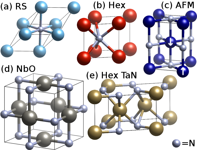
Stoichiometric nitrides with formula MN, where M is a transition metal from groups IV-VI are most often experimentally synthesized and found to be stable at room temperature in the rock-salt (RS) structure (Fig. 1(a)) Gall et al. (1998); Seo et al. (2005); Fillit et al. (1991); Mei et al. (2015); Brauer (1960); Terao (1971). Table 1 summarizes our DFT calculations of energies and mechanical stabilities of RS and other structures for these nitrides. For group IV nitrides, the RS structure is predicted to be stable and the calculated lattice parameters are in good agreement with experiment Gall et al. (1998); Fillit et al. (1991); Seo et al. (2005) (within 1 %). In this case, the mechanical stability of the structure is indicated by the calculated phonon spectra (shown in SI) containing no imaginary frequencies, which is summarized in Table 1 by a positive well-defined zero-point energy (ZPE).
However, we find the experimentally prevalent RS structure to be mechanically unstable for nitrides of groups V and VI, indicated by imaginary frequencies in the phonon dispersion relations (in the SI) and an undefined ZPE in Table 1, in agreement with previous theoretical calculations on these materials Isaev et al. (2007). The primary reason for this discrepancy is that DFT calculations predict energies and forces at zero temperature, and it turns out for these materials that the room-temperature stable phases are unstable at zero temperature. Specifically for VN, the RS structure is unstable towards a tetragonal distortion below 250 K, and is only stabilized above this temperature by anharmonic lattice vibrations.Mei et al. (2015) Predicting electron-phonon and optical properties, fully from first principles, for phases that are mechanically unstable at zero temperature is not currently practical with available methods, and will be a subject of future work. Instead, we will focus here on zero-temperature-stable phases of these materials.
We find that all group V and VI nitrides have a mechanically stable hexagonal (Hex) phase (Fig. 1(b)) with a lower energy than the unstable RS structure. Specifically, for TaN, the stable structure is the more complex hexagonal structure shown in Fig. 1(e), in good agreement with experiment Terao (1971) with predicted lattice parameters within 1 %.
The group VI nitrides have an additional complication, where the experimentally observed RS structures, for example in WN, could be stabilized by vacancy formation Balasubramanian et al. (2016). Once again, performing ab initio electron-phonon and optical response calculations on large unit cells with a low concentration of vacancies is currently impractical. Instead, following Ref. 39 we focus on a symmetric high-concentration limit (25 %) of ion-pair vacancies in the RS structure, which results in the NbO structure shown in Fig. 1(d). We find this structure to be mechanically stable for all group VI nitrides, and to be the lowest energy structure for MoN and WN. It is however not stable for group V nitrides, for which only the Hex phases are found to be stable at zero temperature.
Finally, for CrN, the RS structure is stabilized by a tetragonal distortion with anti-ferromagnetic (AFM) order, as shown in Fig. 1(c) and is in agreement with previous theoretical predictions Zhou et al. (2014). This structure is very close in energy to the Hex structure, and lower in energy than the NbO structure. We also find that all structures other than the RS CrN prefer to remain non-magnetic. We perform ab initio plasmonic response and hot carrier calculations for all the mechanically stable structures discussed above: the RS structure for group IV, the Hex structures for group V, and the Hex and NbO structures for group VI nitrides, except CrN, where we focus on the two low-energy Hex and AFM structures.
III.2 Resistivity
We start with ab initio calculations of the resistivity; the near-equilibrium transport of charge carriers in these materials, which is also an important constituent of the optical / plasmonic response below. We use a linearized Boltzmann equation with a full-band relaxation-time approximation Brown et al. (2016a); Gunst et al. (2016), where the conductivity tensor is calculated as
| (1) |
where the integral over the Brillouin Zone (BZ) is carried out using Monte Carlo sampling with values, with all terms in the integrand calculated efficiently using the Wannier representation as discussed in the Methods section. Above, the Fermi occupation energy derivative selects carriers near the Fermi level, the band velocities are just the diagonal terms in the aforementioned velocity matrix elements () and denotes tensor / outer product. The final term is the momentum relaxation time, whose inverse (momentum scattering rate) is given by Fermi’s golden rule as
| (2) |
where the terms in the product, in order, represent energy conservation, occupation factors, the electron-phonon matrix elements and the angle between initial and final electron velocities after scattering. The sum over accounts for phonon absorption and emission processes, and we point out once again that all quantities above originate from DFT via the Wannier representation. See Ref. 24 and 21 for further details.
To ease analysis, we also define two averaged quantities not directly used in the resistivity calculation above. First, we define the average Fermi velocity by
| (3) |
where the Fermi occupation derivative selects all states near the Fermi level that contribute to conduction (within a few of ). Second, we define the average ‘Drude’ relaxation time,
| (4) |
which is just an average of the per-state momentum relaxation time near the Fermi level, weighted by the band velocity squared because that determines the contribution to the conductivity above.
| TMN | Phase | [fs] | [106m/s] | Resistivity, [nm] | |
| Calc | Expt (S) | ||||
| TiN | RS | 6.9 | 0.72 | 123 | 129Mei et al. (2013) |
| ZrN | RS | 5.8 | 1.01 | 114 | 120Mei et al. (2013) |
| HfN | RS | 5.4 | 1.08 | 112 | 142Mei et al. (2013) |
| VN | Hex | 99. | 0.28 | 191 | |
| NbN | Hex | 68. | 0.36 | 381 | |
| TaN | Hex | 37. | 0.73 | 139 | |
| CrN | Hex | 17.6 | 0.33 | 99 | |
| AFM | 9.5 | 0.47 | 351 | ||
| MoN | Hex | 4.2 | 0.63 | 220 | |
| NbO | 6.9 | 0.53 | 265 | ||
| WN | Hex | 3.0 | 0.72 | 249 | |
| NbO | 8.9 | 0.67 | 190 | ||
Table 2 reports the calculated resistivity values, average Fermi velocities and Drude relaxation time for all mechanically stable structures of the nine TMN materials considered here. For the group IV nitrides, where RS structure is theoretically stable at zero temperature and also experimentally stable at room temperature, the calculated resistivities are in excellent agreement with experimental measurements on single-crystalline / epitaxially-grown materials Mei et al. (2013). However, for all other nitrides, experimental values in the literature span several orders of magnitude, ranging from nm, while the theoretical predictions remain on the same order of magnitude as the group IV nitrides. This is because these materials tend to adopt primarily non-stoichiometric configurations with very large concentrations of defects that substantially increase carrier scattering.
In comparison, note that silver has a resistivity of 16 nm, a Drude relaxation time of 35 fs and a Fermi velocity m/s Brown et al. (2016a). Therefore, the nitrides have resistivities that are typically one order of magnitude higher, but they differ drastically in the combination of factors that lead to that result. The cubic-based structures (RS, AFM and NbO) all have shorter relaxation times and Fermi velocities comparable to silver, while the hexagonal structures have comparable or longer relaxation times than silver, but smaller Fermi velocities. This, in turn, is caused by a lower density-of-states at the Fermi level for the hexagonal nitrides, which lowers the rate of electron-phonon scattering. In particular, we predict hexagonal VN to exhibit a momentum relaxation time that is almost three times larger than silver!
III.3 Optical response and carrier generation
Next, we calculate the complex dielectric function for each of the mechanically-stable TMN structures as
| (5) |
consisting of the Drude intraband term with and calculated in the previous section, and contributions from direct and phonon-assisted transitions. From Fermi’s Golden rule, the imaginary part of the direct (interband) contribution is
| (6) |
while that of the phonon-assisted (intraband) contribution is
| (7) |
where all the energies, occupation factors and matrix elements are as defined above and evaluated form a Wannier representation, and where is a test unit vector along the field direction to conveniently express the tensorial result. The corresponding direct parts are evaluated by the Kramers-Kronig relation. The energy-conserving -functions are broadened to Lorentzians with width equal to the sum of the initial and final carrier linewidths (), which are also evaluated ab initio as indicated in the carrier transport section below, and is used for eliminating singular contributions in the phonon-assisted result. By histogramming integrands in the above expressions with respect to , we also evaluate the energy distributions of carriers generated upon absorption. See Ref. 24 for further details and demonstration of the quantitative accuracy of this method for conventional plasmonic metals.
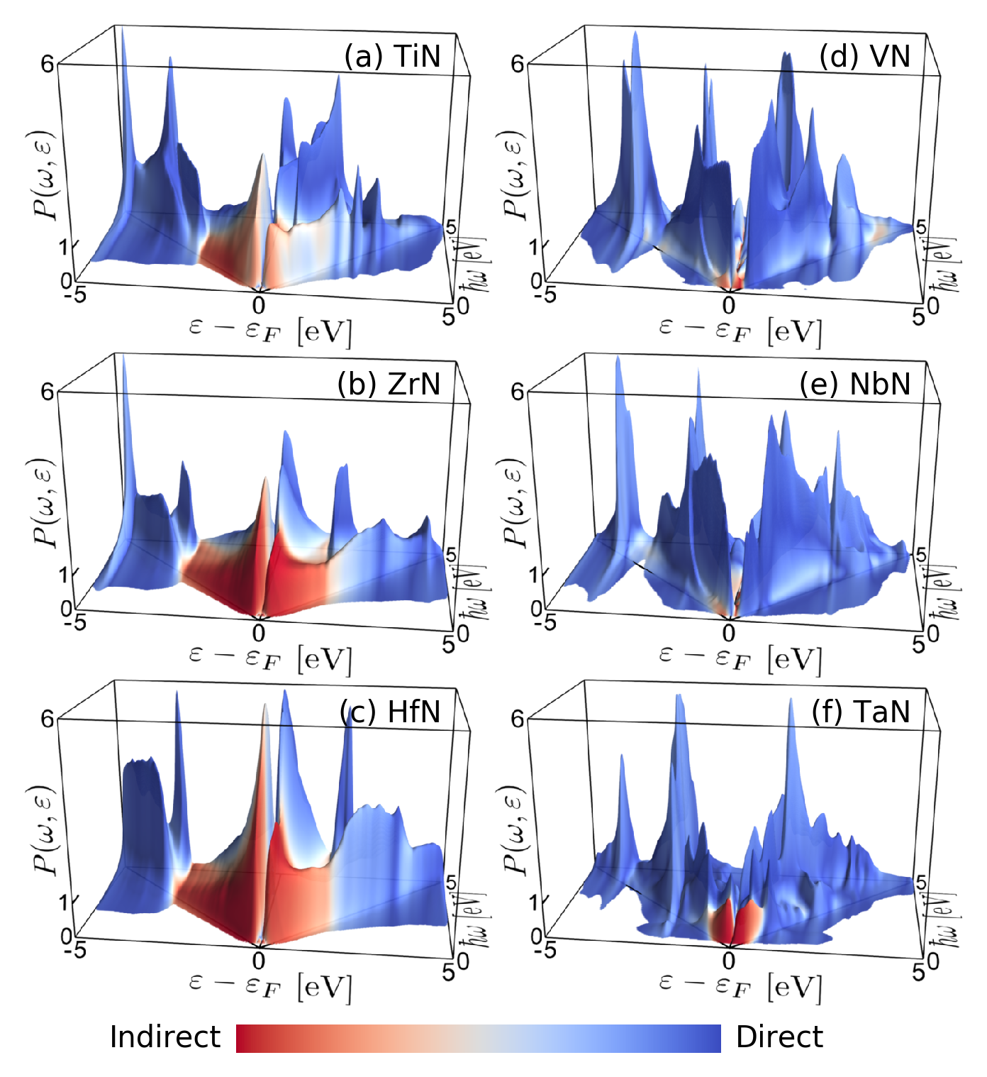
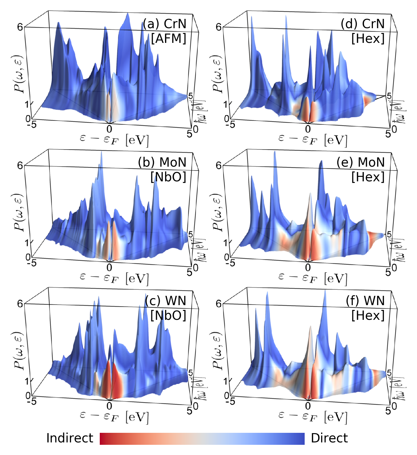
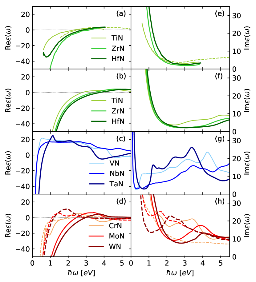
Figure 2 shows the predicted dielectric functions for the stable TMN phases The RS group IV nitrides and the Hex group VI nitrides all exhibit a wide energy window of negative corresponding to plasmonic behavior, ranging from 2 eV for CrN to almost 4 eV for HfN. These windows are comparable to about 2.6 eV for gold and 3.4 eV for silver calculated using the same method Brown et al. (2016b); the experimental values for the noble metals are about 0.2 - 0.3 eV larger. The corresponding where crosses zero is also quite low, indicating excellent plasmonic behavior over this energy range extending across the visible region and into the near UV. In contrast, group V nitrides and the NbO/AFM-structure group VI nitrides exhibit a much narrower plasmonic window, less than 1 eV. However, within that narrow window, the group V nitrides exhibit substantially lower due to the much longer Drude relaxation time discussed in the previous section.
The calculated dielectric functions are in good agreement with experimental data for the group IV nitrides in RS structure Naik et al. (2011); Patsalas et al. (2015) shown in Fig. 2(a,e). In particular, the energy at which crosses zero, demarcating the plasmonic window for these metals, agrees with experiment within 0.2 eV for TiN and ZrN, and within 1 eV for HfN. This agreement is well within the sample to sample variation of measured optical properties of TMNs, which are extremely sensitive to stoichiometry, impurities and growth methods Naik et al. (2011); Patsalas et al. (2015). These issues are particularly severe for group V and VI TMNs Patsalas et al. (2018); Balasubramanian et al. (2016) and comparison to experiment for those materials require explicit treatment of defective systems, a subject of ongoing work. Finally, note that the calculated dielectric functions of the group IV nitrides are in good agreement with previous calculations that treated the intraband contributions empirically Kumar et al. (2016); see Ref. 22 for a detailed comparison of the predicted plasmonic properties of these nitrides with noble metals.
Here, we instead focus on the plasmonic hot carrier properties of these nitrides, where plasmonic loss is not an issue, but rather the design goal. Fig. 3 and 4 show the predicted energy distributions of generated hot carriers for each material as a function of plasmon/photon energy, and also indicates the relative contributions of phonon-assisted and direct transitions. The group IV nitrides with wide plasmonic windows generate carriers predominantly by phonon-assisted transitions at lower photon energies, which then switches to predominantly direct transitions above an interband threshold, analogously to the noble metals Brown et al. (2016a). All remaining nitrides support direct transitions at almost all energies and the dominance of phonon-assisted transitions is narrow, roughly parallel to the plasmonic windows.
Additionally, in contrast to the noble metals, the carrier distributions in all cases, direct or indirect, exhibit complex features due to the more complicated band structures and do not clearly have regions of uniform carrier energy distributions as the noble metals do Brown et al. (2016a). While the carrier distributions are ‘spiky’, they appear to cover the entire energy range extending from photon energy below the Fermi level to photon energy above it (the small contributions beyond the photon energy are due to carrier broadening, and are allowed for these short-lived carriers by the uncertainty principle). However, they are not perfectly symmetrical between electrons and holes, just as in the noble metals, and it is important to know if the energy distributions are electron or hole-dominant in order to decide suitability for -type collection / reductive photochemistry or -type collection / oxidative photochemistry respectively.
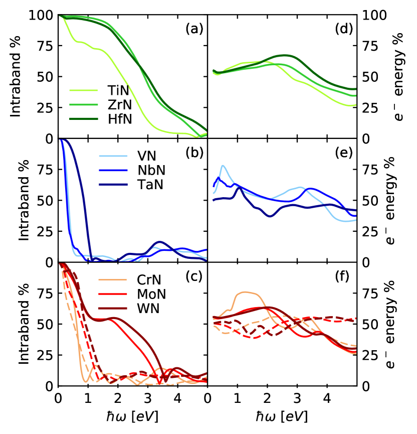
Figure 5 summarizes the relative contribution from intraband transitions and energy dominance of electrons versus holes for the TMNs. The cross-over from intraband to direct transitions on the left panels correlates very well with the end of the plasmonic window ( in Fig. 2). Correspondingly direct (interband) carrier generation becomes important for the RS group IV nitrides, Hex MoN and Hex WN above 3 eV, and above 1 eV for all other nitrides. The indirect (intraband) processes distribute energy between hot electrons and holes roughly evenly, while direct transitions tend to bias the carrier distribution towards holes, just as for the noble metals Sundararaman et al. (2014), but to a lesser extent. The underlying reason for this remains that these direct transitions are predominantly from metal -bands below the Fermi level to just above the Fermi level. Also, interestingly the energy bias swings slightly towards the electrons for photon energies just below the interband threshold (indicated by the humps in Fig. 5(d-f)), which arises because of the (small) asymmetry in the conduction band density of states from below the Fermi level to above it. Altogether, all these nitrides are capable of generating both hot electrons and holes with distributions extending mostly all the way to the photon energy, almost irrespective of the photon energy.
III.4 Carrier transport
Finally, we calculate the lifetimes and mean-free paths of hot carriers generated in these materials which are the determining factors for the efficiency of plasmonic hot carrier applications. The electron-phonon contribution to the inverse lifetime is
| (8) |
identical to the momentum relaxation rate given by (2), except without the factor accounting for the angle between initial and final velocities. The electron-electron contribution is calculated using
| (9) |
where are density matrices in the plane-wave basis with reciprocal lattice vectors , and is the inverse dielectric matrix calculated in the Random Phase Approximation. See Ref. 44 for a detailed introduction to this method and Ref. 24 for our specific implementation details. The net carrier lifetime is , and from it we calculate the carrier linewidths for the broadening in (6) and (7) above, as well as the mean free path .
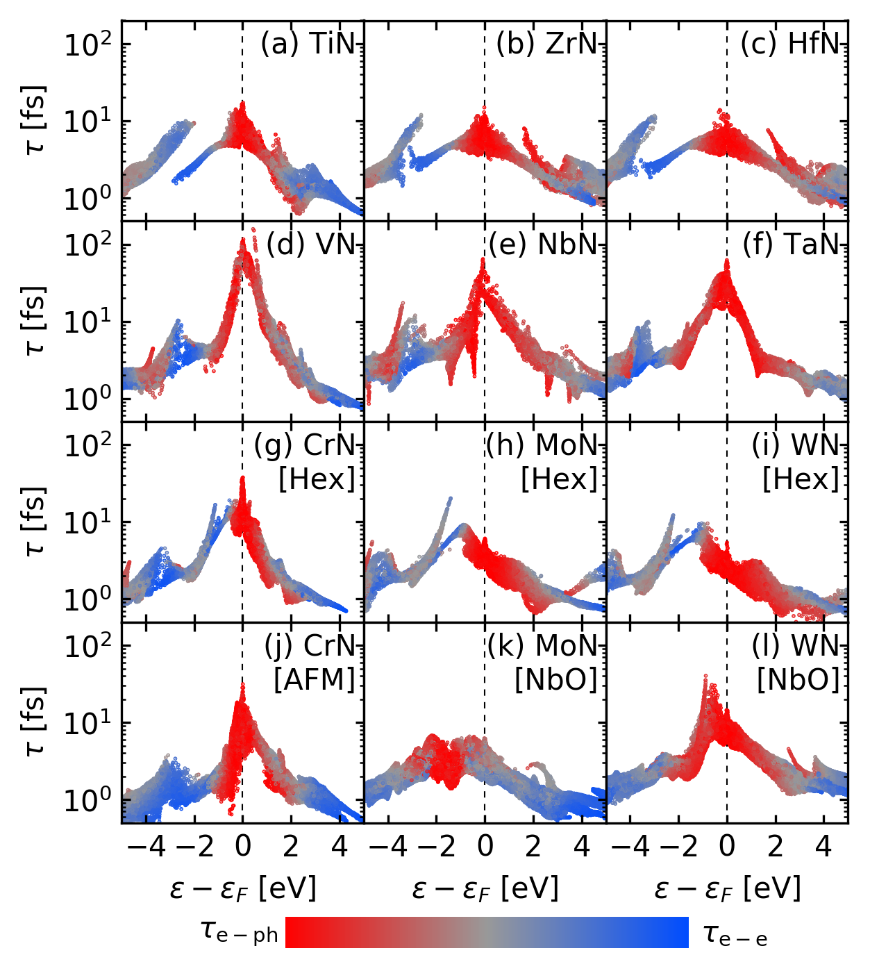
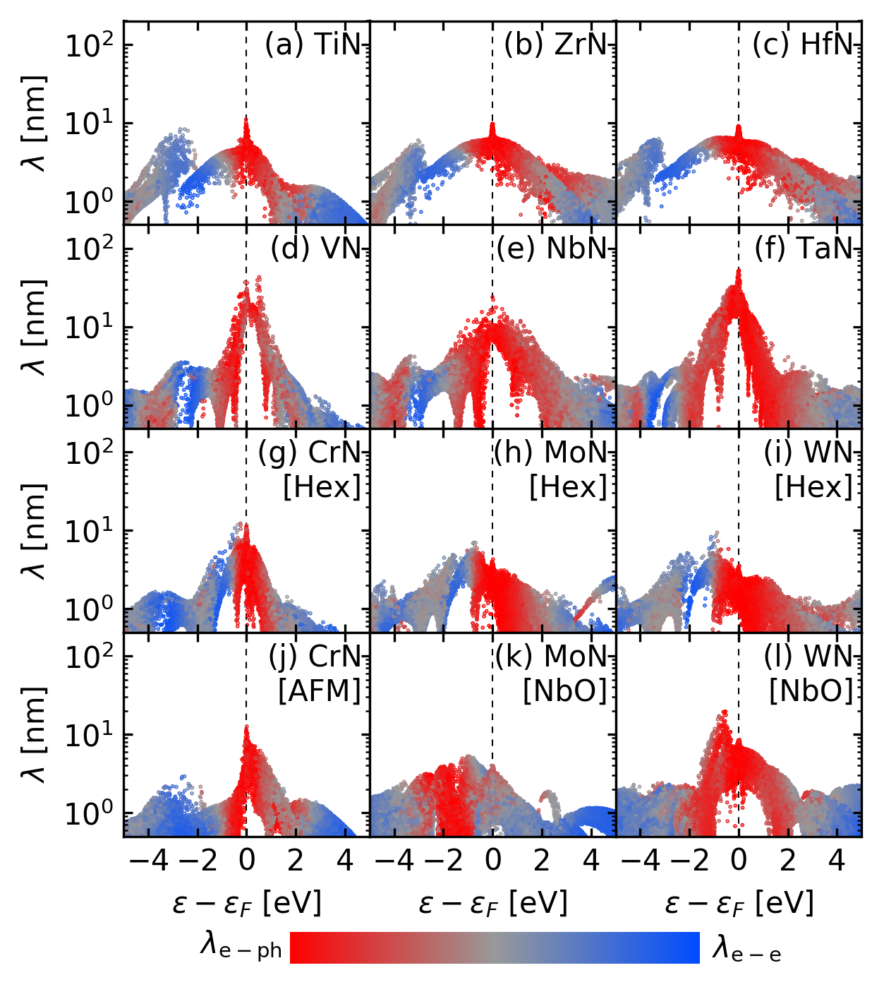
Figures 6 and 7 respectively show the calculated lifetimes and mean free paths for all TMNs as a function of carrier energy away from Fermi level, indicating relative contributions of electron-electron and electron-phonon processes using a color scale. In each panel of both figures, the maximum lifetime (or mean free path) typically occurs near the Fermi level, where it is dominated by electron-phonon scattering and where the phase space for electron-electron scattering is negligible. The lifetime rapidly diminishes with increasing energy away from the Fermi level due to the increased phase space for electron-electron scattering, clearly indicated by the change from red to blue in the figures. This behavior is qualitatively similar to that of the noble metals Brown et al. (2016a), except that the shapes of the fall-off are more complicated here on account of more complex density of states profiles compared to the free-electron-like ones in the noble metals. Sharp discontinuities seen in Fig. 6(a-c,h,i) correspond to new bands opening up at that energy, and states near that band edge have a long life-time due to reduced scattering phase space. However, the corresponding panels in Fig. 7 do not exhibit these discontinuities, or strongly suppress them, because carrier velocities near these band edges are small.
Figures 6(d-f) show that group V TMNs have the highest life times for carriers near the Fermi level, almost an order of magnitude greater than most of the other nitrides. In fact, just as was the case for the Drude relaxation time (Table 2), NbN and TaN have comparable lifetimes to silver, the highest among noble metals, and VN exceeds it by a factor of two. Among the remaining nitrides, WN in the NbO phase and the two CrN structures exhibit the highest lifetimes, approaching 20-30 fs. The corresponding advantage for group V nitrides over the rest in terms of mean free paths (Fig. 7(d-f)) is less striking, because of an overall lower band velocity near the Fermi level. As discussed above, this also resulted in similar resistivities compared to other nitrides despite substantially longer relaxation times. In terms of mean free path, TaN leads with maximum values exceeding 40 nm, with NbN and VN close behind at around 30 nm. However, the lifetimes drop below 10 fs and mean free paths below 10 nm for carrier energies exceeding 1 eV across the board, similar to what we found for graphene and its heterostructures Narang et al. (2017). The nitrides fall behind silver in this regard, where the carrier lifetimes and mean free paths decline more gradually with energy from the Fermi level Brown et al. (2016a).
IV Conclusions
Using ab initio calculations of optical response, hot carrier generation and carrier transport, we show that plasmonic transition metal nitrides are promising candidates for efficient hot carrier extraction. Group IV and VI nitrides exhibit wider frequency windows for plasmonic response, while group V nitrides exhibit the best carrier transport properties. Our completely parameter-free predictions for the resistivity of these materials are in excellent agreement with experimental results on stoichiometric nitrides, currently available for group IV nitrides.
Hot carrier generation is dominated by direct transitions for optical frequencies in most of the nitrides, and intraband transitions become important primarily at infrared frequencies for the group IV nitrides. Generated carrier energy distributions tend to be more evenly distributed between electrons and holes compared to noble metals, and are only slightly biased towards holes when interband transitions dominate.
Finally, in terms of carrier transport, hexagonal VN exhibits the highest carrier lifetime, far exceeding silver, but on account of the lower Fermi velocity in VN, TaN exhibits the highest carrier mean free path, comparable to silver. High-energy () carrier transport in these materials is somewhat inferior to the noble metals, but an important advantage of these refractory plasmonic materials remains that they can be stabilized at much smaller dimensions, potentially circumventing limitations due to shorter carrier transport distances.
A key bottleneck in current ab initio studies of hot carrier dynamics is the limitation to structures mechanically stable at zero temperature, inherent because of the perturbative nature of the calculations relative to the perfect crystal. This precluded calculations of rock-salt structures of materials such as VN, which are mechanically stable at room temperature but unstable at zero temperature. More generally, phonon-related properties of TMNs could be sensitive to temperature even when the room-temperature structures are stable at zero temperature. The capability to account for finite temperature effective force matrices and electron-phonon matrix elements from ab initio molecular dynamics simulations is therefore an important future direction in theoretical calculations of hot carrier dynamics in general, and to plasmonic nitrides in particular.
Supplemental Information
The supplemental information includes plots of electronic band structures, density of states, phonon band structures, and phonon density of states for all nitride structures considered above.
Acknowledgments
RS acknowledges startup funding from the Department of Materials Science and Engineering at Rensselaer Polytechnic Institute. Calculations were performed on the BlueGene/Q supercomputer in the Center for Computational Innovations (CCI) at Rensselaer Polytechnic Institute.
References
- Molarius et al. (1987) J. Molarius, A. Korhonen, E. Harju, and R. Lappalainen, Surf. Coat. Tech. 33, 117 (1987).
- Budke et al. (1999) E. Budke, J. Krempel-Hesse, H. Maidhof, and H. Schüssler, Surf. Coat. Tech. 112, 108 (1999).
- Toth (1971) L. E. Toth, Transition Metal Carbides and Nitrides (Academic Press, 1971).
- McIntyre et al. (1990) D. McIntyre, J. E. Greene, G. Håkansson, J. Sundgren, and W. Münz, J. Appl. Phys. 67, 1542 (1990).
- Chun et al. (2001) J.-S. Chun, J. R. A. Carlsson, P. Desjardins, D. B. Bergstrom, I. Petrov, J. E. Greene, C. Lavoie, C. C. Jr., and L. Hultman, J. Vacuum Sci. Tech. A 19, 182 (2001).
- Östling et al. (1986) M. Östling, S. Nygren, C. Petersson, H. Norström, R. Buchta, H.-O. Blom, and S. Berg, Thin Solid Films 145, 81 (1986).
- Patsalas et al. (1999) P. Patsalas, C. Charitidis, S. Logothetidis, C. A. Dimitriadis, and O. Valassiades, J. Appl. Phys. 86, 5296 (1999).
- Gotoh et al. (2001) Y. Gotoh, Y. Kashiwagi, M. Nagao, T. Kondo, H. Tsuji, and J. Ishikawa, J. Vacuum Sci. Tech. B 19, 1373 (2001).
- Hardy and Hulm (1954) G. F. Hardy and J. K. Hulm, Phys. Rev. 93, 1004 (1954).
- Guler et al. (2014) U. Guler, A. Boltasseva, and V. M. Shalaev, Science 344, 263 (2014).
- Naik et al. (2012) G. V. Naik, J. L. Schroeder, X. Ni, A. V. Kildishev, T. D. Sands, and A. Boltasseva, Opt. Mater. Express 2, 478 (2012).
- Patsalas et al. (2018) P. Patsalas, N. Kalfagiannis, S. Kassavetis, G. Abadias, D. V. Bellas, C. Lekka, and E. Lidorikis, Mater. Sci. Eng. R Rep. Accepted (2018), DOI: 10.1016/j.mser.2017.11.001.
- Mei et al. (2013) A. B. Mei, A. Rockett, L. Hultman, I. Petrov, and J. E. Greene, J. Appl. Phys. 114, 193708 (2013).
- Zia et al. (2006) R. Zia, J. A. Schuller, A. Chandran, and M. L. Brongersma, Mater. Today 9, 20 (2006).
- Im et al. (2014) H. Im, H. Shao, Y. I. Park, V. M. Peterson, C. M. Castro, R. Weissleder, and H. Lee, Nature Biotech. 32, 490 (2014).
- Hyde et al. (2009) G. K. Hyde, S. D. McCullen, S. Jeon, S. M. Stewart, H. Jeon, E. G. Loboa, and G. N. Parsons, Biomed. Mater. 4, 025001 (2009).
- Guler et al. (2015) U. Guler, V. M. Shalaev, and A. Boltasseva, Materials Today 18, 227 (2015).
- Brongersma et al. (2015) M. L. Brongersma, N. J. Halas, and P. Nordlander, Nature Nanotech. 10 (2015).
- Moskovits (2015) M. Moskovits, Nature Nanotech. 10 (2015).
- Narang et al. (2016a) P. Narang, R. Sundararaman, and H. A. Atwater, Nanophotonics 5, 96 (2016a).
- Narang et al. (2017) P. Narang, L. Zhao, S. Claybrook, and R. Sundararaman, Adv. Opt. Mater. 5, 1600914 (2017).
- Kumar et al. (2016) M. Kumar, N. Umezawa, S. Ishii, and T. Nagao, ACS Photonics 3, 43 (2016).
- Sundararaman et al. (2014) R. Sundararaman, P. Narang, A. S. Jermyn, W. A. Goddard III, and H. A. Atwater, Nature Commun. 5, 12 (2014).
- Brown et al. (2016a) A. M. Brown, R. Sundararaman, P. Narang, W. A. Goddard, and H. A. Atwater, ACS Nano 10, 957 (2016a).
- Narang et al. (2016b) P. Narang, R. Sundararaman, A. S. Jermyn, W. A. Goddard, and H. A. Atwater, J. Phys. Chem. C 120, 21056 (2016b).
- Brown et al. (2016b) A. M. Brown, R. Sundararaman, P. Narang, W. A. Goddard III, and H. A. Atwater, Phys. Rev. B 94, 075120 (2016b).
- Brown et al. (2017) A. M. Brown, R. Sundararaman, P. Narang, A. Schwartzberg, W. A. Goddard III, and H. A. Atwater, Phys. Rev. Lett. 118, 087401 (2017).
- Sundararaman et al. (2017) R. Sundararaman, K. Letchworth-Weaver, K. Schwarz, D. Gunceler, Y. Ozhabes, and T. A. Arias, SoftwareX 6, 278 (2017).
- Perdew et al. (1996) J. P. Perdew, K. Burke, and M. Ernzerhof, Phys. Rev. Lett. 77, 3865 (1996).
- Schlipf and Gygi (2015) M. Schlipf and F. Gygi, Comput. Phys. Commun. 196, 36 (2015).
- Souza et al. (2001) I. Souza, N. Marzari, and D. Vanderbilt, Phys. Rev. B 65, 035109 (2001).
- Gall et al. (1998) D. Gall, I. Petrov, N. Hellgren, L. Hultman, J. E. Sundgren, and J. E. Greene, J. Appl. Phys. 84, 6034 (1998).
- Fillit et al. (1991) R. Fillit, A. Perry, and C. Strandberg, Thin Solid Films 197, 47 (1991).
- Seo et al. (2005) H.-S. Seo, T.-Y. Lee, I. Petrov, J. E. Greene, and D. Gall, J. Appl. Phys. 97, 083521 (2005).
- Mei et al. (2015) A. B. Mei, O. Hellman, N. Wireklint, C. M. Schlepütz, D. G. Sangiovanni, B. Alling, A. Rockett, L. Hultman, I. Petrov, and J. E. Greene, Phys. Rev. B 91, 054101 (2015).
- Brauer (1960) G. Brauer, J. Less Common Metals 2, 131 (1960), conference on Niobium, Tantalum, Molybdenum and Tungsten.
- Terao (1971) N. Terao, Jap. J. Appl. Phys. 10, 248 (1971).
- Isaev et al. (2007) E. I. Isaev, S. I. Simak, I. A. Abrikosov, R. Ahuja, Y. K. Vekilov, M. I. Katsnelson, A. I. Lichtenstein, and B. Johansson, J. Appl. Phys. 101, 123519 (2007).
- Balasubramanian et al. (2016) K. Balasubramanian, S. Khare, and D. Gall, Phys. Rev. B 94, 174111 (2016).
- Zhou et al. (2014) L. Zhou, F. Körmann, D. Holec, M. Bartosik, B. Grabowski, J. Neugebauer, and P. H. Mayrhofer, Phys. Rev. B 90, 184102 (2014).
- Gunst et al. (2016) T. Gunst, T. Markussen, K. Stokbro, and M. Brandbyge, Phys. Rev. B 93, 035414 (2016).
- Naik et al. (2011) G. V. Naik, J. Kim, and A. Boltasseva, Opt. Mater. Express 1, 1090 (2011).
- Patsalas et al. (2015) P. Patsalas, N. Kalfagiannis, and S. Kassavetis, Materials 8, 3128 (2015).
- Ladstädter et al. (2004) F. Ladstädter, U. Hohenester, P. Puschnig, and C. Ambrosch-Draxl, Phys. Rev. B 70, 235125 (2004).